1
File Number
2892.4
HA-2406
30MHz, Digitally Selectable Four Channel
Operational Amplifier
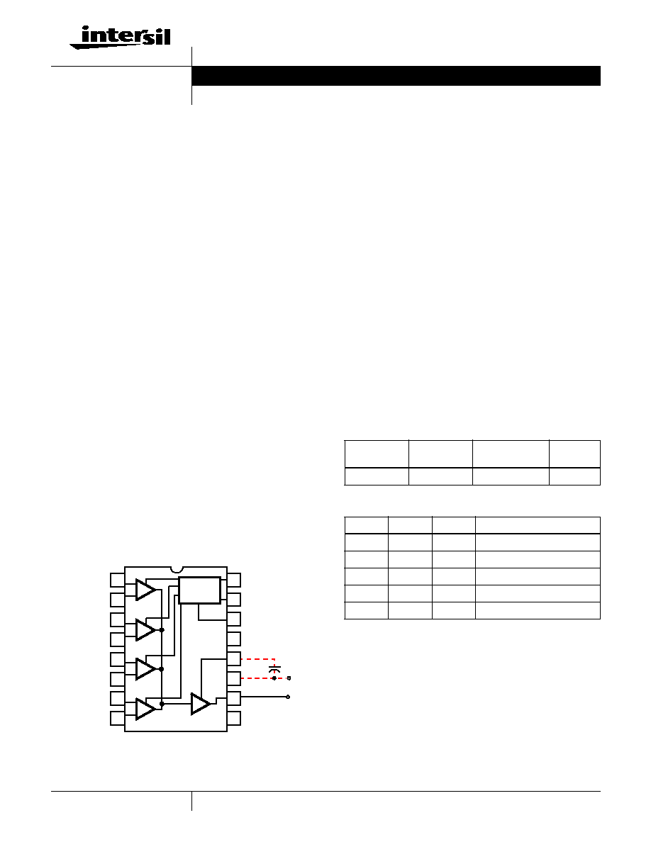
The HA-2406 is a monolithic device consisting of four op
amp input stages that can be individually connected to one
output stage by decoding two TTL lines into four channel
select signals. In addition to allowing each channel to be
addressed, an enable control disconnects all input stages
from the output stage when asserted low.
Each input-output combination of the HA-2406 is designed
to be a 20V/
µ
s, 30MHz gain-bandwidth amplifier that is
stable at a gain of ten. By connecting one external 15pF
capacitor all amplifiers are compensated for unity gain
operation. The compensation lead may also be used to limit
the output swing to TTL levels through suitable clamping
diodes and divider networks (see Application Note AN514).
Dielectric isolation and short-circuit protected output stages
contribute to the quality and durability of the HA-2406. When
used as a simple amplifier, its dynamic performance is very
good and when its added versatility is considered, the
HA-2406 is unmatched in the analog world. It can replace a
number of individual components in analog signal
conditioning circuits for digital signal processing systems. Its
advantages include saving board space and reducing power
supply requirements.
During Disable Mode V
OUT
goes to V-. For high output
impedance during Disable, see HA2444.
For further design ideas, see Application Note AN514.
Pinout
HA-2406
(PDIP)
TOP VIEW)
Features
∑ TTL Compatible Inputs
∑ Single Capacitor Compensation
∑ Low Crosstalk . . . . . . . . . . . . . . . . . . . . . . . . . . . . . -110dB
∑ High Slew Rate. . . . . . . . . . . . . . . . . . . . . . . . . . . . 20V/
µ
s
∑ Low Offset Current . . . . . . . . . . . . . . . . . . . . . . . . . . . 5nA
∑ Offset Voltage . . . . . . . . . . . . . . . . . . . . . . . . . . . . . . . 7mV
∑ High Gain-Bandwidth . . . . . . . . . . . . . . . . . . . . . . . 30MHz
∑ High Input Impedance . . . . . . . . . . . . . . . . . . . . . . . 30M
∑ Compensation Pin for Unity Gain Capability
Applications
∑ Digital Control Of
- Analog Signal Multiplexing
- Op Amp Gains
- Oscillator Frequencies
- Filter Characteristics
- Comparator Levels
14
15
16
9
13
12
11
10
1
2
3
4
5
7
6
8
3
OUTPUT AMP
ENABLE
D0
D1
GND
COMP
V+
OUTPUT
V-
4
1
2
+IN3
-IN3
+IN4
-IN4
-IN1
+IN1
+IN2
-IN2
3
DECODE
CONTROL
+
-
+
-
+
-
+
-
Ordering Information
PART NO.
TEMP RANGE
(
o
C)
PACKAGE
PKG. NO.
HA3-2406-5
0 to 75
16 Ld PDIP
E16.3
TRUTH TABLE
D1
D0
EN
SELECTED CHANNEL
L
L
H
1
L
H
H
2
H
L
H
3
H
H
H
4
X
X
L
None, V
OUT
goes to V-
Data Sheet
April 1999
CAUTION: These devices are sensitive to electrostatic discharge; follow proper IC Handling Procedures.
1-888-INTERSIL or 321-724-7143
|
Copyright
©
Intersil Corporation 1999
2
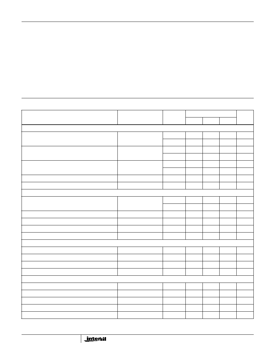
Absolute Maximum Ratings
T
A
= 25
o
C
Thermal Information
Supply Voltage Between V+ and V- Terminals. . . . . . . . . . . . . . 45V
Differential Input Voltage . . . . . . . . . . . . . . . . . . . . . . . . . . V
SUPPLY
Output Current . . . . . . . . . . . Short Circuit Protected (I
SC
< ±
33mA)
Operating Conditions
Temperature Range
HA-2406-5 . . . . . . . . . . . . . . . . . . . . . . . . . . . . . . . . 0
o
C to 75
o
C
Thermal Resistance (Typical, Note 1)
JA
(
o
C/W)
PDIP Package . . . . . . . . . . . . . . . . . . . . . . . . . . . . .
80
Maximum Junction Temperature (Plastic Package) . . . . . . . . .150
o
C
Maximum Storage Temperature Range . . . . . . . . . . -65
o
C to 150
o
C
Maximum Lead Temperature (Soldering 10s) . . . . . . . . . . . . 300
o
C
CAUTION: Stresses above those listed in "Absolute Maximum Ratings" may cause permanent damage to the device. This is a stress only rating and operation of the
device at these or any other conditions above those indicated in the operational sections of this specification is not implied.
NOTE:
1.
JA
is measured with the component mounted on an evaluation PC board in free air.
Electrical Specifications
Test Conditions: V
SUPPLY
=
±
15.0V, Unless Otherwise Specified. Digital Inputs: V
IL
= +0.5V, V
IH
= +2.4V. Lim-
its apply to each of the four channels, when addressed.
PARAMETER
TEST
CONDITIONS
TEMP (
o
C)
HA-2406-5
UNITS
MIN
TYP
MAX
INPUT CHARACTERISTICS
Offset Voltage
25
-
7
10
mV
Full
-
-
12
mV
Bias Current (Note 7)
25
-
50
250
nA
Full
-
-
500
nA
Offset Current (Note 7)
25
-
5
50
nA
Full
-
-
100
nA
Input Resistance (Note 7)
25
-
30
-
M
Common Mode Range
Full
±
9.0
-
-
V
TRANSFER CHARACTERISTICS
Large Signal Voltage Gain
R
L
= 2k
V
OUT
= 20V
P-P
25
40
150
-
kV/V
Full
20
-
-
kV/V
Common Mode Rejection Ratio
V
CM
=
±
5V
Full
74
80
-
dB
Gain Bandwidth Product (Notes 2, 9)
25
15
30
-
MHz
Gain Bandwidth Product (Notes 3, 9)
25
3
6
-
MHz
Minimum Stable Gain
C
COMP
= 0
10
-
-
V/V
OUTPUT CHARACTERISTICS
Output Voltage Swing
R
L
= 2k
Full
±
10.0
±
12.0
-
V
Output Current
V
OUT
=
±
10V
25
10
15
-
mA
Full Power Bandwidth (Notes 2, 8, 9)
V
OUT
= 20V
P-P
25
240
320
-
kHz
Full Power Bandwidth (Notes 3, 8)
V
OUT
= 20V
P-P
25
64
95
-
kHz
TRANSIENT RESPONSE (Note 10)
Rise Time (Note 3)
V
OUT
= 200mV
PEAK
25
-
30
100
ns
Overshoot (Note 3)
V
OUT
= 200mV
PEAK
25
-
25
40
%
Slew Rate (Notes 2, 9)
V
OUT
= 10V
P-P
25
15
20
-
V/
µ
s
Slew Rate (Note 3)
V
OUT
= 10V
P-P
25
4
6
-
V
µ
s
Settling Time (Notes 3, 4)
V
OUT
= 10V
P-P
25
-
2.0
3.5
µ
s
HA-2406
3
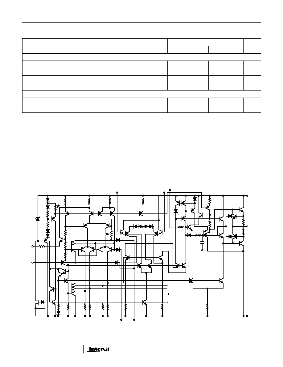
Schematic Diagram
CHANNEL SELECT CHARACTERISTICS
Digital Input Current
V
IN
= 0V
Full
-
1
1.5
mA
Digital Input Current
V
IN
= +5.0V
Full
-
15
-
nA
Output Delay (Notes 5, 9)
25
-
150
300
ns
Crosstalk (Note 6)
25
-74
-110
-
dB
POWER SUPPLY CHARACTERISTICS
Supply Current
25
-
4.8
7.0
mA
Power Supply Rejection Ratio
V
S
=
±
10V to
±
20V
Full
74
90
-
dB
NOTES:
2. A
V
= +10, C
COMP
= 0, R
L
= 2k
, C
L
= 50pF.
3. A
V
= +1, C
COMP
= 15pF, R
L
= 2k
, C
L
= 50pF.
4. To 0.1% of final value.
5. To 10% of final value; output then slews at normal rate to final value.
6. Unselected input to output; V
IN
=
±
10V.
7. Unselected channels have approximately the same input parameters.
8. Full power Bandwidth based on slew rate measurement using:
.
9. Sample tested.
10. See Figure 13 for test circuit.
Electrical Specifications
Test Conditions: V
SUPPLY
=
±
15.0V, Unless Otherwise Specified. Digital Inputs: V
IL
= +0.5V, V
IH
= +2.4V. Lim-
its apply to each of the four channels, when addressed. (Continued)
PARAMETER
TEST
CONDITIONS
TEMP (
o
C)
HA-2406-5
UNITS
MIN
TYP
MAX
FPBW
Slew Rate
2
V
PEAK
-----------------------------
=
ENABLE
GND
OUT
R
2
2.4K
R
4
22.9K
Q
1
Q
3
Q
4
Q
6
Q
7
Q
8
R
1
1.6K
R
3
1.8K
Q
2
Q
5
R
5
8.0K
R
6
2.0K
R
35
1.6K
R
7
5.6K
Q
10
Q
11
Q
13
Q
12
Q
15
Q
14
R
8
4K
Q
16
R
9
1.5K
R
10
10K
R
11
10K
VA
VC
Q
17
VB
Q
18
Q
19
Q
20
VD
R
12
1.6K
Q
28
VE
R
13
0.8K
Q
22
R
15
10K
R
16
10K
Q
21
Q
26
Q
27
R
14
10K
Q
29
Q
23
Q
24
Q
25
Q
30
Q
32
Q
33
Q
102
Q
34
Q
38
R
18
2.0K
Q
103
Q
35
Q
31
Q
36
Q
37
Q
39
Q
40
Q
41
Q
79
Q
81
Q
82
Q
84
Q
80
Q
83
Q
86
Q
89
Q
88
R
35
0.75K
Q
85
Q
98
Q
92
R
30
1.2K
C
1
9.0pF
V+
Q
93
Q
42
R
19
1.6K
TO ADDITIONAL
INPUT STAGES
R
29
0.4K
Q
90
Q
91
R
33
4K
Q
97
Q
100
Q
99
Q
95
Q
94
+V
CC
-V
EE
R
31
36.5
R
32
34
Q
96
COMP
IN-
IN+
D1
D0
R
17
1.6K
Q
87
R
34
1.6K
Q
101
Q
9
Diagram Includes: One Input Stage, Decode Control, Bias Network, and Output Stage
HA-2406
4
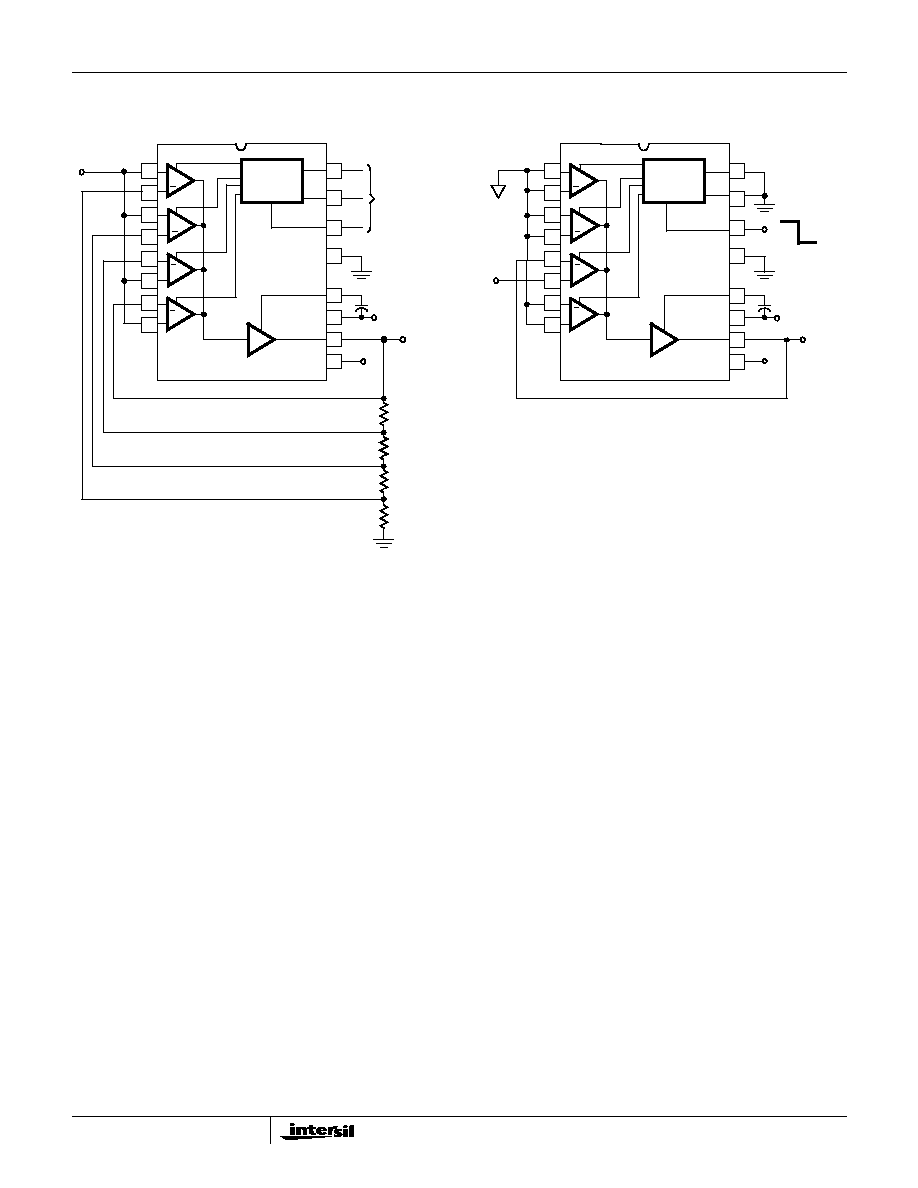
For more examples, see Intersil Application Note AN514.
Typical Applications
FIGURE 1. HA-2406 AMPLIFIER, NONINVERTING
PROGRAMMABLE GAIN
FIGURE 2. HA-2406 SAMPLE AND HOLD
+ 2
1K
500
500
ENABLE
GND
COMP
OUTPUT
AMP
V-
13
8
1
2
3
4
5
7
6
V+
+
4
+
3
+
1
14
15
16
12
11
10
9
+
D1
D0
15pF
IN
2K
-15V
DECODE/
CONTROL
DIGITAL
DIGITAL
GROUND
CONTROL
+ 15V
OUT
1
ENABLE
GND
COMP
OUTPUT
AMP
V-
13
8
1
2
3
4
5
7
6
V+
+
4
+
3
+
+2
14
15
16
12
11
10
9
D1
D0
-15V
DIGITAL
GROUND
+15V
C
OUT
S
H
IN
DECODE/
CONTROL
Sample Charging Rate
I
1
C
-----
V s
/
=
Hold Drift Rate
1
2
C
------
V s
/
=
Switch Pedestal Error
Q
C
----
V
=
I1
150 x 10-6A
I
2
200 x 10
-9
A at 25
o
C
600 x 10
-9
A at -55
o
C
100 x 10
-9
A at 125
o
C
Q
2 x 10
-12
C
HA-2406
5
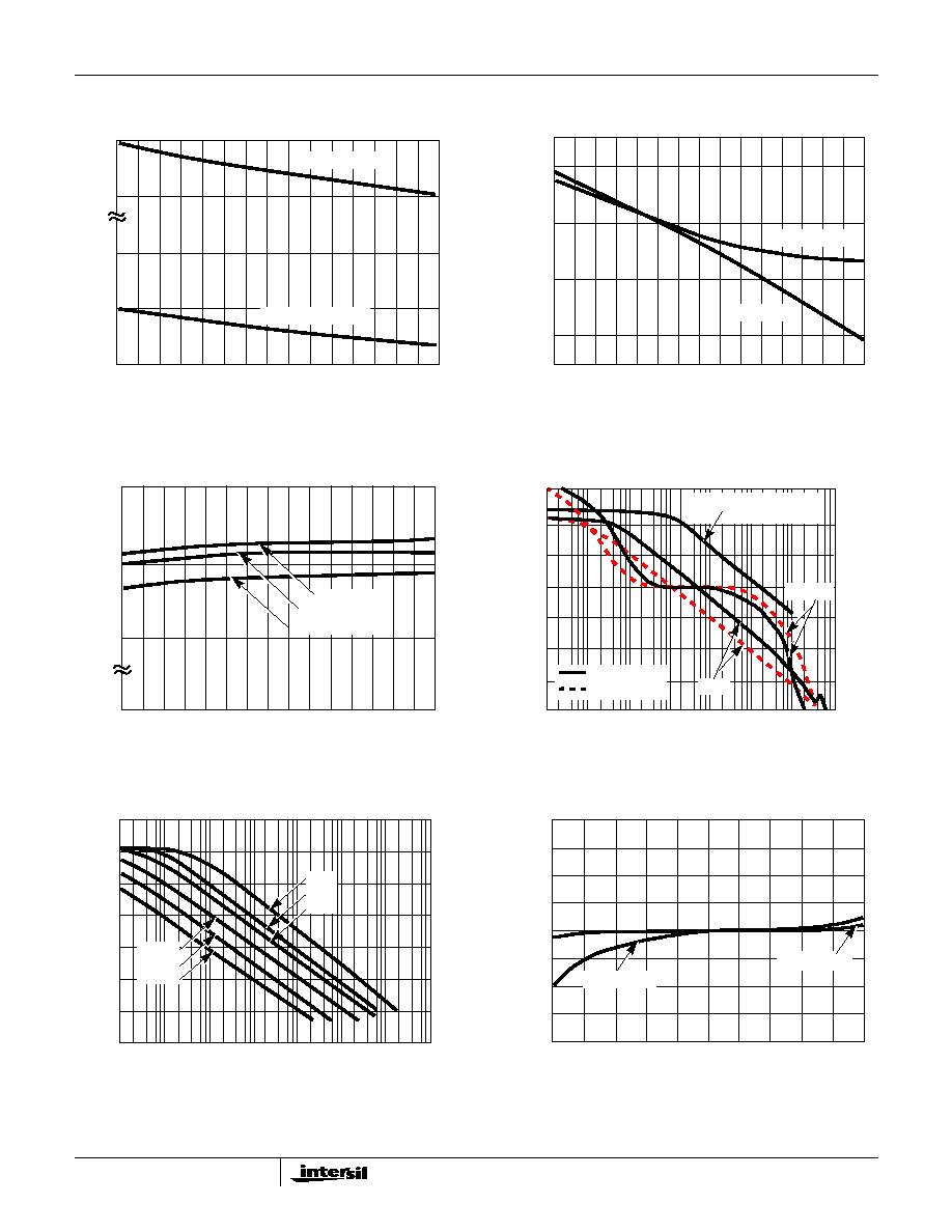
Typical Performance Curves
FIGURE 3. INPUT BIAS CURRENT AND OFFSET CURRENT
vs TEMPERATURE
FIGURE 4. NORMALIZED AC PARAMETERS vs
TEMPERATURE
FIGURE 5. POWER SUPPLY CURRENT vs TEMPERATURE
FIGURE 6. OPEN LOOP FREQUENCY AND PHASE RESPONSE
FIGURE 7. FREQUENCY RESPONSE vs C
COMP
FIGURE 8. NORMALIZED AC PARAMETERS vs SUPPLY
VOLTAGE
BIAS CURRENT
OFFSET CURRENT
TEMPERATURE (
o
C)
OFFSET CURRENT (nA)
0
25
50
75
0
5
10
40
60
BANDWIDTH
SLEW RATE
TEMPERATURE (
o
C)
NORMALIZED V
ALUE REFERRED T
O
25
o
C
0
25
50
75
0.9
1.0
V
S
=
±
20V
V
S
=
±
15V
V
S
=
±
10V
TEMPERATURE (
o
C)
SUPPL
Y CURRENT (mA)
4.50
4.25
4.0
0
0
25
50
75
C
COMP
= 0pF
PHASE
C
COMP
= 15pF
GAIN
OPEN LOOP V
O
L
T
A
GE GAIN (dB)
FREQUENCY (Hz)
10
100
1K
10K
100K
1M
10M
100M
CROSSTALK REJECTION,
A
V
= +1
-20
0
20
40
60
80
100
120
0
30
60
90
120
150
180
210
PHASE (DEGREES)
FREQUENCY (Hz)
10
100
1K
10K
100K
1M
10M
100M
OPEN LOOP V
O
L
T
A
GE GAIN (dB)
-20
0
20
40
60
80
100
120
1000pF
300pF
100pF
30pF
15pF
0pF
SLEW RATE
BANDWIDTH
SUPPLY VOLTAGE (V)
±
10
±
20
±
15
0.8
0.9
1.0
1.1
1.2
NORMALIZED V
ALUE REFERRED T
O
±
15V
HA-2406
6
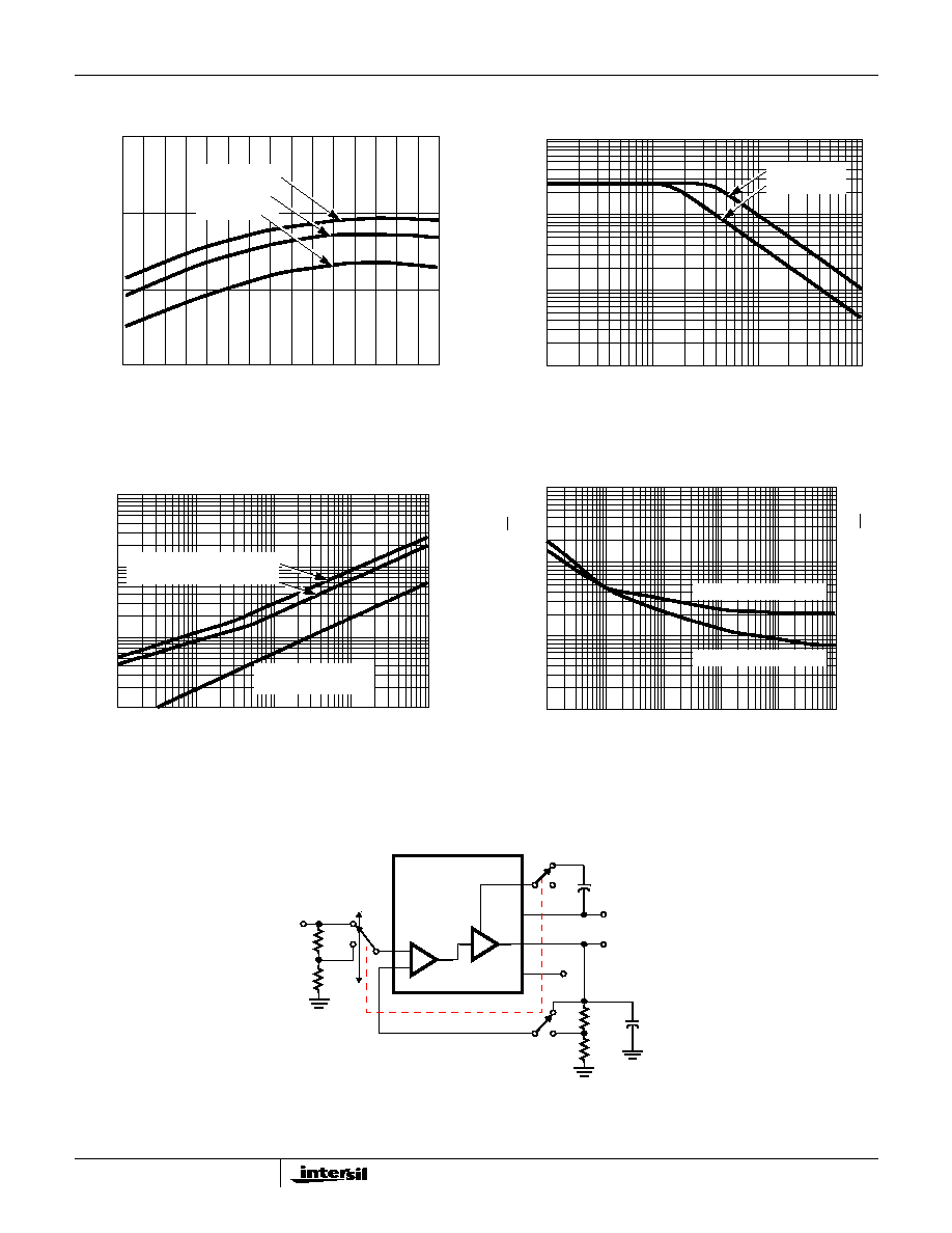
FIGURE 9. OPEN LOOP VOLTAGE GAIN vs TEMPERATURE
FIGURE 10. OUTPUT VOLTAGE SWING vs FREQUENCY
FIGURE 11. EQUIVALENT INPUT NOISE vs BANDWIDTH
FIGURE 12. INPUT NOISE vs FREQUENCY
FIGURE 13. SLEW RATE AND TRANSIENT RESPONSE
Typical Performance Curves
(Continued)
V
S
=
±
20V
V
S
=
±
15V
V
S
=
±
10V
TEMPERATURE (
o
C)
0
25
50
75
GAIN (dB)
105
100
FREQUENCY (Hz)
10K
100K
1M
10M
OUTPUT SWING (V
P-P
)
0.1
1.0
10
20
C
COMP
= 0pF
C
COMP
= 15pF
100Hz
1kHz
10kHz
100kHz
1MHz
UPPER 3dB FREQUENCY (LOWER 3dB FREQUENCY-10Hz)
BROADBAND NOISE CHARACTERISTICS
INPUT NOISE (
µ
V)
100
10
1.0
0.1
0K SOURCE RESISTANCE
10K SOURCE RESISTANCE
THERMAL NOISE OF
10K RESISTOR
1
100
1K
10K
100K
10
FREQUENCY (Hz)
INPUT NOISE CURRENT (pA/
Hz)
INPUT NOISE V
O
L
T
A
GE (nV/
Hz)
1000
100
10
1
10
1
0.1
0.01
INPUT NOISE VOLTAGE
INPUT NOISE CURRENT
COMP
A
V
= 1
IN
15pF
+15.0V
OUT
SELECTED
CHANNEL
-15.0V
1800
200
+
-
A
V
= 10
50pF
45
5
HA-2406

7
All Intersil semiconductor products are manufactured, assembled and tested under ISO9000 quality systems certification.
Intersil semiconductor products are sold by description only. Intersil Corporation reserves the right to make changes in circuit design and/or specifications at any time with-
out notice. Accordingly, the reader is cautioned to verify that data sheets are current before placing orders. Information furnished by Intersil is believed to be accurate and
reliable. However, no responsibility is assumed by Intersil or its subsidiaries for its use; nor for any infringements of patents or other rights of third parties which may result
from its use. No license is granted by implication or otherwise under any patent or patent rights of Intersil or its subsidiaries.
For information regarding Intersil Corporation and its products, see web site www.intersil.com
Sales Office Headquarters
NORTH AMERICA
Intersil Corporation
P. O. Box 883, Mail Stop 53-204
Melbourne, FL 32902
TEL: (321) 724-7000
FAX: (321) 724-7240
EUROPE
Intersil SA
Mercure Center
100, Rue de la Fusee
1130 Brussels, Belgium
TEL: (32) 2.724.2111
FAX: (32) 2.724.22.05
ASIA
Intersil (Taiwan) Ltd.
7F-6, No. 101 Fu Hsing North Road
Taipei, Taiwan
Republic of China
TEL: (886) 2 2716 9310
FAX: (886) 2 2715 3029
HA-2406
Dual-In-Line Plastic Packages (PDIP)
NOTES:
1. Controlling Dimensions: INCH. In case of conflict between English and
Metric dimensions, the inch dimensions control.
2. Dimensioning and tolerancing per ANSI Y14.5M-1982.
3. Symbols are defined in the "MO Series Symbol List" in Section 2.2 of
Publication No. 95.
4. Dimensions A, A1 and L are measured with the package seated in JE-
DEC seating plane gauge GS-3.
5. D, D1, and E1 dimensions do not include mold flash or protrusions.
Mold flash or protrusions shall not exceed 0.010 inch (0.25mm).
6. E and
are measured with the leads constrained to be perpendic-
ular to datum
.
7. e
B
and e
C
are measured at the lead tips with the leads unconstrained.
e
C
must be zero or greater.
8. B1 maximum dimensions do not include dambar protrusions. Dambar
protrusions shall not exceed 0.010 inch (0.25mm).
9. N is the maximum number of terminal positions.
10. Corner leads (1, N, N/2 and N/2 + 1) for E8.3, E16.3, E18.3, E28.3,
E42.6 will have a B1 dimension of 0.030 - 0.045 inch (0.76 - 1.14mm).
e
A
-C-
C
L
E
e
A
C
e
B
e
C
-B-
E1
INDEX
1 2 3
N/2
N
AREA
SEATING
BASE
PLANE
PLANE
-C-
D1
B1
B
e
D
D1
A
A2
L
A1
-A-
0.010 (0.25)
C
A
M
B S
E16.3
(JEDEC MS-001-BB ISSUE D)
16 LEAD DUAL-IN-LINE PLASTIC PACKAGE
SYMBOL
INCHES
MILLIMETERS
NOTES
MIN
MAX
MIN
MAX
A
-
0.210
-
5.33
4
A1
0.015
-
0.39
-
4
A2
0.115
0.195
2.93
4.95
-
B
0.014
0.022
0.356
0.558
-
B1
0.045
0.070
1.15
1.77
8, 10
C
0.008
0.014
0.204
0.355
-
D
0.735
0.775
18.66
19.68
5
D1
0.005
-
0.13
-
5
E
0.300
0.325
7.62
8.25
6
E1
0.240
0.280
6.10
7.11
5
e
0.100 BSC
2.54 BSC
-
e
A
0.300 BSC
7.62 BSC
6
e
B
-
0.430
-
10.92
7
L
0.115
0.150
2.93
3.81
4
N
16
16
9
Rev. 0 12/93