
1
File Number
2909.4
HA-5142
Dual, 400kHz, Ultra-Low
Power Operational Amplifier
The HA-5142 ultra-low power operational amplifier provides
AC and DC performance characteristics similar to or better
than most general purpose amplifiers while only drawing
1/30 of the supply current of most general purpose
amplifiers. In applications which require low power
dissipation and good AC electrical characteristics, this
device offers the industry's best speed/power ratio.
The HA-5142 provides accurate signal processing by virtue
of its low input offset voltage (2mV), low input bias current
(45nA), high open loop gain (100kV/V) and low noise
(20nV/
Hz), for low power operational amplifiers. These
characteristics coupled with a 1.5V/
µ
s slew rate and a
400kHz bandwidth make the HA-5142 ideal for use in low
power instrumentation, audio amplifier and active filter
designs. The wide range of supply voltages (3V to 30V) also
allow this amplifier to be very useful in low voltage battery
powered equipment. This device is also tested and
guaranteed at both
±
15V and single ended +5V supplies.
This amplifier is available with industry standard pinouts
which allow the HA-5142 to be interchangeable with most
other dual operational amplifiers. For military grade product
refer to the HA-5142/883 data sheet.
Features
∑ Low Supply Current . . . . . . . . . . . . . . . . . . . . . 45
µ
A/Amp
∑ Wide Supply Voltage Range Single . . . . . . . . . 3V to 30V
- or Dual
. . . . . . . . . . . . . . . . . . . . . . . . . . . . . .±
1.5V to
±
15V
∑ High Slew Rate. . . . . . . . . . . . . . . . . . . . . . . . . . . 1.5V/
µ
s
∑ High Gain . . . . . . . . . . . . . . . . . . . . . . . . . . . . . . 100kV/V
∑ Unity Gain Stable
Applications
∑ Portable Instruments
∑ Meter Amplifiers
∑ Telephone Headsets
∑ Microphone Amplifiers
∑ Instrumentation
- For Further Design Ideas See Application Note 544
Pinout
HA-5142 (PDIP, CERDIP)
TOP VIEW
Ordering Information
PART
NUMBER
TEMP. RANGE
(
o
C)
PACKAGE
PKG. NO.
HA3-5142-5
0 to 75
8 Ld PDIP
E8.3
HA7-5142-2
-55 to 125
8 Ld CERDIP
F8.3A
OUT1
+IN1
V-
2
3
4
1
V+
OUT2
+IN2
7
6
5
8
+
1
2
-IN1
-IN2
-
+
-
Data Sheet
April 1999
CAUTION: These devices are sensitive to electrostatic discharge; follow proper IC Handling Procedures.
1-888-INTERSIL or 321-724-7143
|
Copyright
©
Intersil Corporation 1999
2
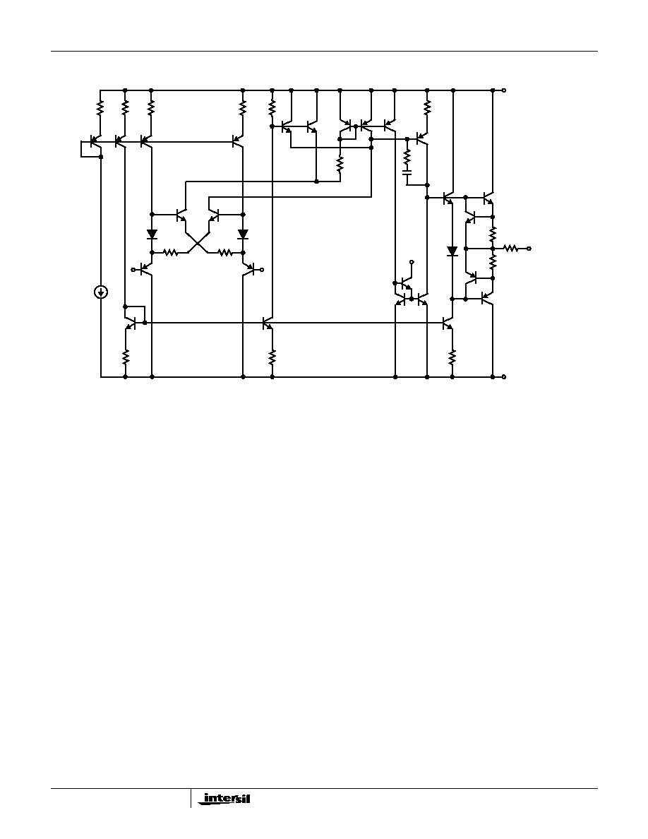
Schematic Diagram
-IN
+IN
V+
V-
OUTPUT
V+
HA-5142
3
Absolute Maximum Ratings
Thermal Information
Supply Voltage Between V+ and V- Terminals. . . . . . . . . . . . . . 35V
Differential Input Voltage . . . . . . . . . . . . . . . . . . . . . . . . . . . . . . . 7V
Output Current . . . . . . . . . . . . . . . . . . . . . . . Short Circuit Protected
Operating Conditions
Temperature Range
HA-5142-5 . . . . . . . . . . . . . . . . . . . . . . . . . . . . . . . . 0
o
C to 75
o
C
HA-5142-2 . . . . . . . . . . . . . . . . . . . . . . . . . . . . . . -55
o
C to 125
o
C
Thermal Resistance (Typical, Note 1)
JA
(
o
C/W)
JC
(
o
C/W)
8 Lead PDIP Package . . . . . . . . . . . . .
120
N/A
8 Lead CERDIP Package . . . . . . . . . . .
135
50
Maximum Junction Temperature (Hermetic Packages). . . . . . . .175
o
C
Maximum Junction Temperature (Plastic Packages) . . . . . . .150
o
C
Maximum Storage Temperature Range . . . . . . . . . . -65
o
C to 150
o
C
Maximum Lead Temperature (Soldering 10s) . . . . . . . . . . . . 300
o
C
CAUTION: Stresses above those listed in "Absolute Maximum Ratings" may cause permanent damage to the device. This is a stress only rating and operation of the
device at these or any other conditions above those indicated in the operational sections of this specification is not implied.
NOTE:
1.
JA
is measured with the component mounted on an evaluation PC board in free air.
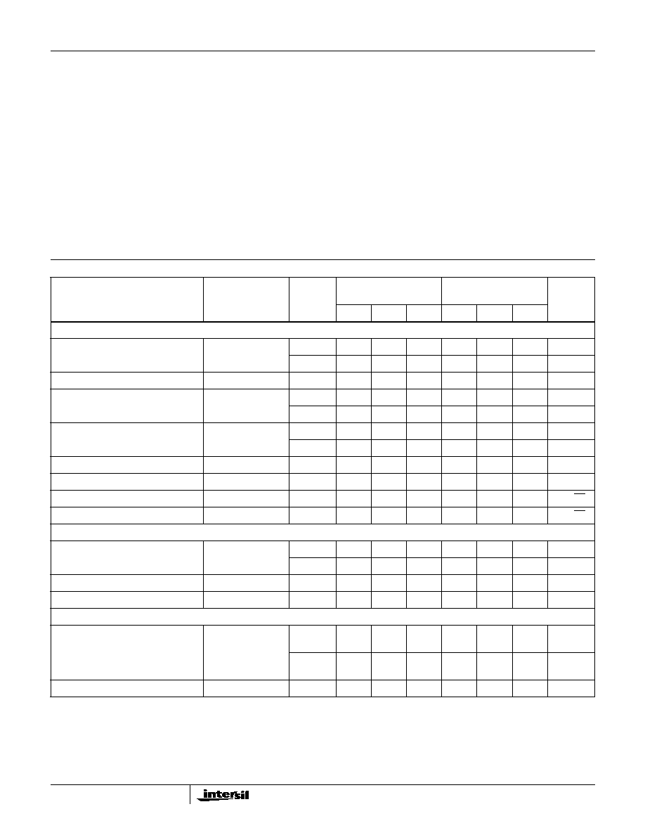
Electrical Specifications
R
S
= 100
, C
L
10pF, Unless Otherwise Specified
PARAMETER
TEST
CONDITIONS
TEMP.
(
o
C)
-2, -5
V+ = +5V, V- = 0V
-2, -5
V+ = +15V, V- = -15V
UNITS
MIN
TYP
MAX
MIN
TYP
MAX
INPUT CHARACTERISTICS
Offset Voltage
Note 11
25
-
2
6
-
2
6
mV
Full
-
-
8
-
-
8
mV
Average Offset Voltage Drift
Full
-
3
-
-
3
-
µ
V/
o
C
Bias Current
Note 11
25
-
45
100
-
45
100
nA
Full
-
-
125
-
-
125
nA
Offset Current
Note 11
25
-
0.3
10
-
0.3
10
nA
Full
-
-
20
-
-
20
nA
Common Mode Range
Full
0 to 3
-
-
±
10
-
-
V
Differential Input Resistance
25
-
0.6
-
-
0.6
-
M
Input Noise Voltage
f = 1kHz
25
-
20
-
-
20
-
nV/
Hz
Input Noise Current
f = 1kHz
25
-
0.25
-
-
0.25
-
pA/
Hz
TRANSFER CHARACTERISTICS
Large Signal Voltage Gain
Notes 2, 4
25
20
100
-
20
100
-
kV/V
Full
15
-
-
15
-
-
kV/V
Common Mode Rejection Ratio
Note 7
Full
77
105
-
77
105
-
dB
Bandwidth
Notes 2, 3
25
-
0.4
-
-
0.4
-
MHz
OUTPUT CHARACTERISTICS
Output Voltage Swing
Notes 2, 10
25
1.0 to
3.8
0.7 to
4.2
-
±
10
±
13
-
V
Full
1.2 to
3.5
0.9 to
4.0
-
±
10
±
13
-
V
Full Power Bandwidth
Notes 2, 4, 8
25
-
240
-
-
24
-
kHz
HA-5142
4
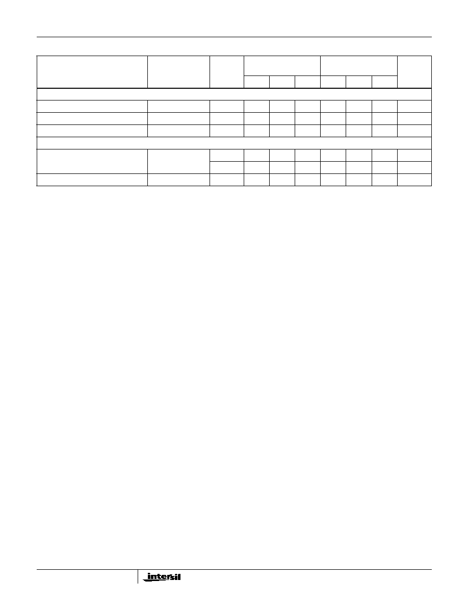
TRANSIENT RESPONSE (Notes 2, 3)
Rise Time
25
-
600
-
-
600
-
ns
Slew Rate
Note 6
25
0.8
1.5
-
0.8
1.5
-
V/
µ
s
Settling Time
Note 5
25
-
10
-
-
10
-
µ
s
POWER SUPPLY CHARACTERISTICS
Supply Current
25
-
45
80
-
100
150
µ
A/Amp
Full
-
-
100
-
-
200
µ
A/Amp
Power Supply Rejection Ratio
Note 9
Full
77
105
-
77
105
-
dB
NOTES:
2. R
L
= 50k
.
3. C
L
= 50pF.
4. V
O
= 1.4 to 2.5V for V
SUPPLY
= +5, 0V; V
O
=
±
10V for V
SUPPLY
=
±
15V.
5. Settling Time is specified to 0.1% of final value for a 3V output step and A
V
= -1 for V
SUPPLY
= +5V, 0V. Output step = 10V for V
SUPPLY
=
±
15V.
6. Maximum input slew rate = 10V/
µ
s.
7. V
CM
= 0 to 3V for V
SUPPLY
= +5, 0V; V
CM
=
±
10V for V
SUPPLY
=
±
15V.
8. Full Power Bandwidth is guaranteed by equation:
.
9.
V
S
= +10V for V
SUPPLY
= +5, 0V;
V
S
=
±
5V for V
SUPPLY
=
±
15V.
10. For V
SUPPLY
= +5, 0V terminate R
L
at +2.5V. Typical output current is
±
3mA.
11. V
O
= 1.4V for V
SUPPLY
= +5V, 0V.
Electrical Specifications
R
S
= 100
, C
L
10pF, Unless Otherwise Specified (Continued)
PARAMETER
TEST
CONDITIONS
TEMP.
(
o
C)
-2, -5
V+ = +5V, V- = 0V
-2, -5
V+ = +15V, V- = -15V
UNITS
MIN
TYP
MAX
MIN
TYP
MAX
FPBW
Slew Rate
2
V
PEAK
---------------------------
=
HA-5142
5
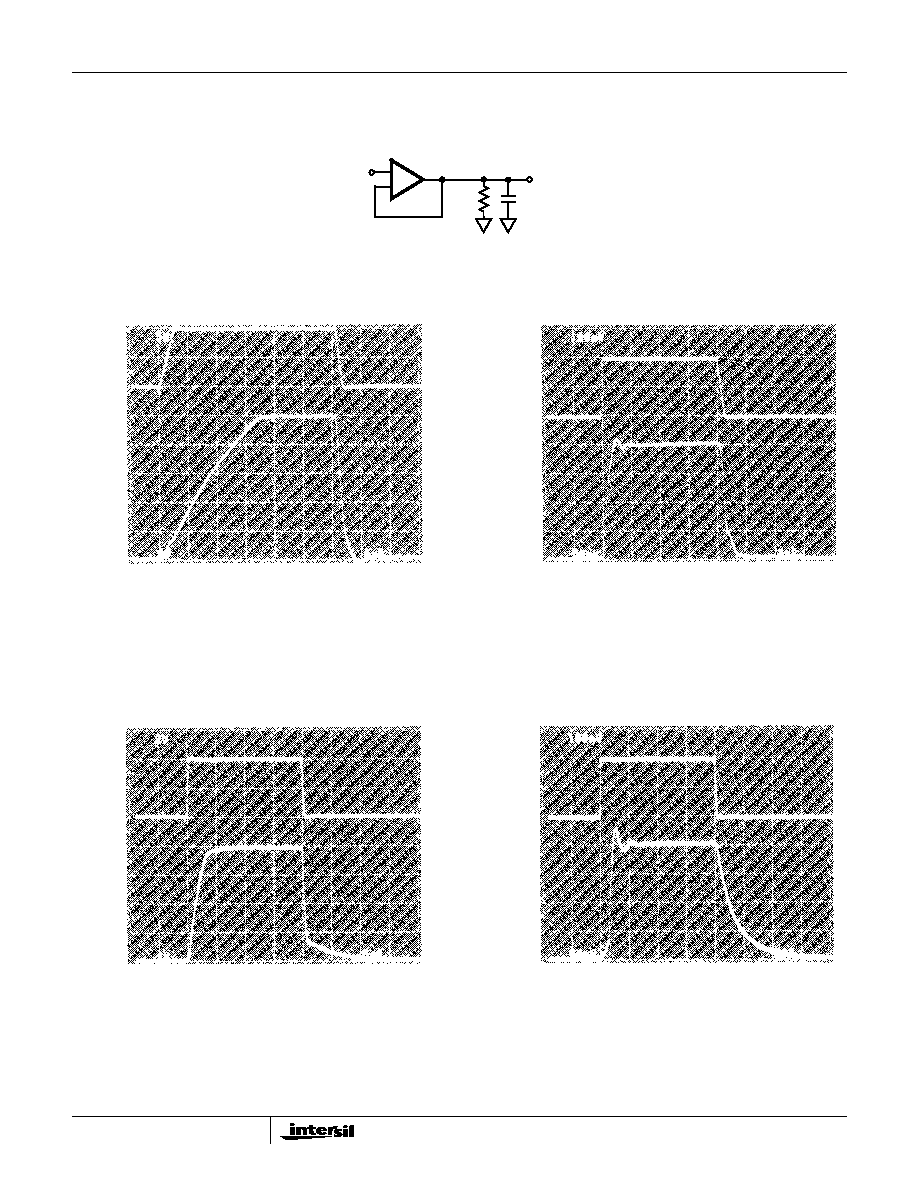
Test Circuits and Waveforms
FIGURE 1. SLEW RATE AND TRANSIENT RESPONSE TEST CIRCUIT
Vertical Scale: Input = 5V/Div.; Output = 2V/Div.
Horizontal Scale: 2
µ
s/Div.
LARGE SIGNAL RESPONSE
Vertical Scale: Input = 100mV/Div.; Output = 50mV/Div.
Horizontal Scale: 2
µ
s/Div.
SMALL SIGNAL RESPONSE
Vertical Scale: Input = 2V/Div.; Output = 1V/Div.
Horizontal Scale: 5
µ
s/Div.
LARGE SIGNAL RESPONSE
Vertical Scale: Input = 100mV/Div.; Output = 50mV/Div.
Horizontal Scale: 5
µ
s/Div.
SMALL SIGNAL RESPONSE
+
IN
OUT
50k
50pF
-
INPUT
OUTPUT
+V
SUPPLY
= +15V, -V
SUPPLY
= -15V
INPUT
OUTPUT
+V
SUPPLY
= +15V, -V
SUPPLY
= -15V
INPUT
OUTPUT
+V
SUPPLY
= +5V, -V
SUPPLY
= 0V
INPUT
OUTPUT
+V
SUPPLY
= +5V, -V
SUPPLY
= 0V
HA-5142
6
Typical Performance Curves
V
S
=
±
2.5V, T
A
= 25
o
C, Unless Otherwise Specified
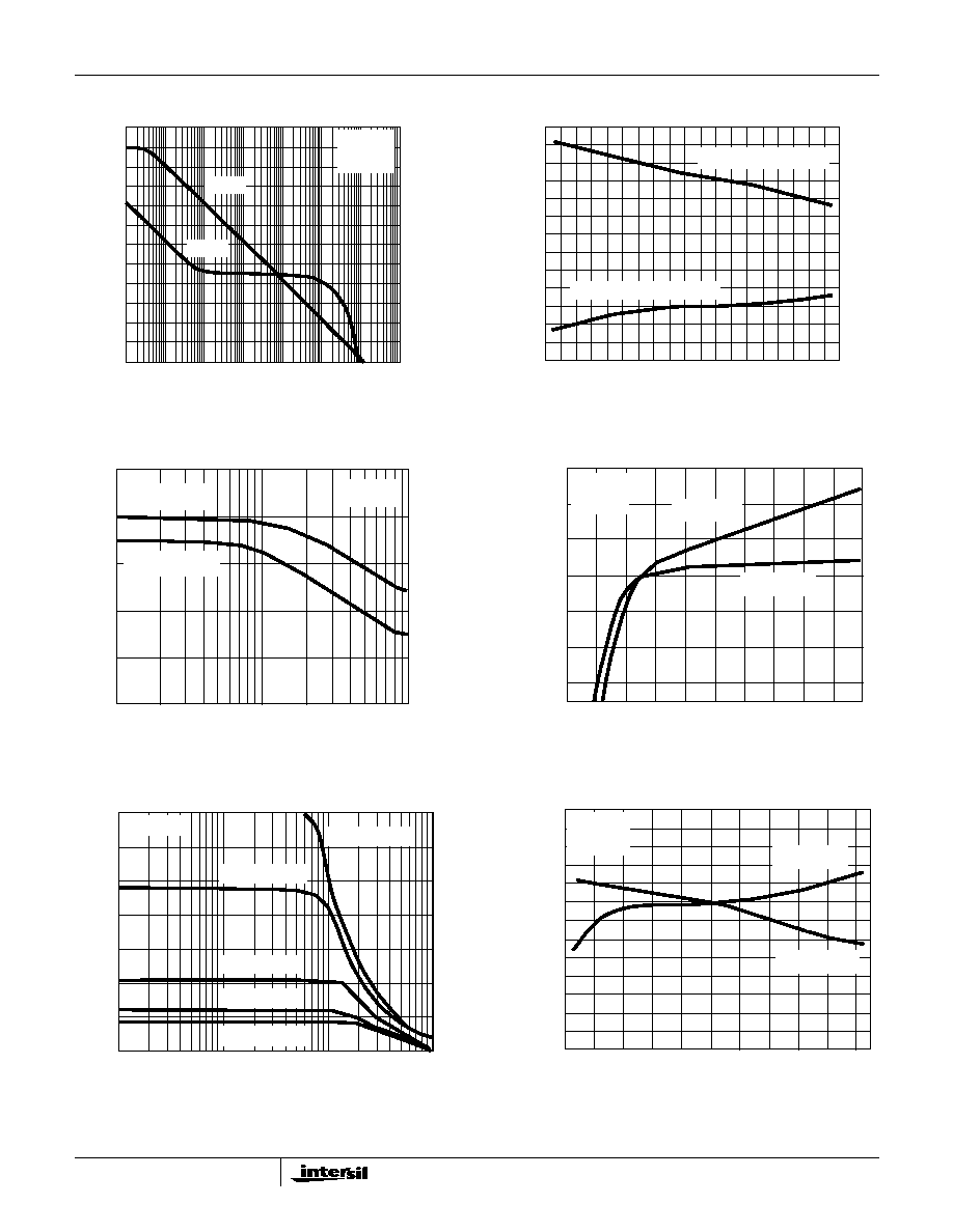
FIGURE 2. OPEN LOOP FREQUENCY RESPONSE
FIGURE 3. INPUT OFFSET CURRENT AND BIAS CURRENT
vs TEMPERATURE
FIGURE 4. BANDWIDTH AND PHASE MARGIN vs LOAD
CAPACITANCE
FIGURE 5. NORMALIZED AC PARAMETERS vs SUPPLY
VOLTAGE
FIGURE 6. OUTPUT VOLTAGE SWING vs FREQUENCY AND
SINGLE SUPPLY VOLTAGE
FIGURE 7. NORMALIZED AC PARAMETERS vs
TEMPERATURE
110
100
90
80
70
60
50
40
30
20
10
0
-10
1
10
100
1K
10K
100K
1M
0
20
40
60
80
100
120
140
160
180
OPEN LOOP V
O
L
T
A
GE GAIN (dB)
PHASE (DEGREES)
FREQUENCY (Hz)
R
L
= 50k
C
L
= 50pF
GAIN
PHASE
TEMPERATURE (
o
C)
70
60
50
40
30
20
10
-60
|I
OS
| (nA)
I
B
(nA)
-40
-20
0
20
40
60
80
100
120
24
20
16
12
8
4
INPUT OFFSET CURRENT
INPUT BIAS CURRENT
100
o
80
o
60
o
40
o
20
o
0
o
10
100
1000
PHASE MARGIN
0.4
0.3
0.2
0.1
UNITY B
AND
WIDTH (MHz)
LOAD CAPACITANCE (pF)
PHASE MARGIN
BANDWIDTH
R
L
= 50k
1.6
1.4
1.2
1.0
0.8
0.6
0.4
0
±
1
±
2
±
3
±
4
±
5
±
6
±
7
±
8
±
9
±
10
SUPPLY VOLTAGE (V)
NORMALIZED A
C
P
ARAMETERS
REFERRED T
O
V
ALUE A
T
±
2.5V
SLEW RATE
BANDWIDTH
R
L
= 50k
C
L
= 50pF
V
SUPPLY
= +2.5V
V
SUPPLY
= +3V
V
SUPPLY
= +5V
V
SUPPLY
= +10V
V
SUPPLY
= +15V
R
L
= 50k
14
12
10
8
6
4
2
0
1K
10K
100K
1M
FREQUENCY (Hz)
OUTPUT V
O
L
T
A
GE SWING (V
P-P
)
R
L
= 50k
C
L
= 50pF
SLEW RATE
BANDWIDTH
1.2
1.1
1.0
0.9
0.8
0.7
0.6
-60
NORMALIZED P
ARAMETERS
REFERRED T
O
V
ALUE A
T
25
o
C
-40
-20
-10
0
20
40
60
80
100
120
TEMPERATURE (
o
C)
HA-5142
7
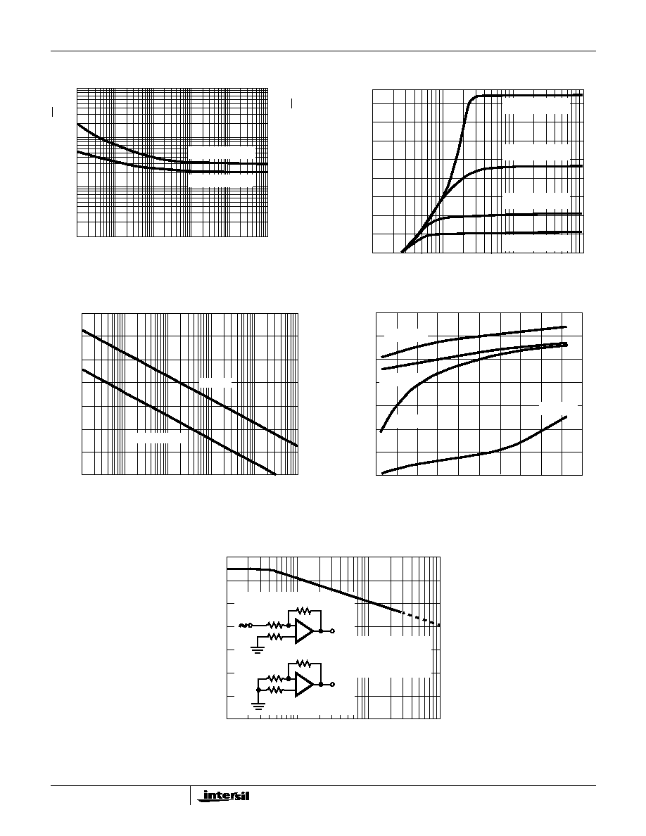
FIGURE 8. INPUT NOISE vs FREQUENCY
FIGURE 9. MAXIMUM OUTPUT VOLTAGE SWING vs LOAD
RESISTANCE AND SINGLE SUPPLY VOLTAGE
FIGURE 10. PSRR AND CMRR vs FREQUENCY
FIGURE 11. POWER SUPPLY CURRENT vs TEMPERATURE
AND SINGLE SUPPLY VOLTAGE
FIGURE 12. CHANNEL SEPARATION vs FREQUENCY
Typical Performance Curves
V
S
=
±
2.5V, T
A
= 25
o
C, Unless Otherwise Specified
(Continued)
NOISE VOLTAGE
NOISE CURRENT
1000
100
10
1
1
1000
100
10
10,000
10
100
1K
10K
100K
FREQUENCY (Hz)
INPUT NOISE V
O
L
T
A
GE (nV/
Hz)
INPUT NOISE CURRENT (10
-15
A/
Hz)
V
SUPPLY
= +10V
16
100
OUTPUT V
O
L
T
A
GE SWING (V
P-P
)
1K
10K
100K
V
SUPPLY
= +20V
V
SUPPLY
= +5V
V
SUPPLY
= +3V
14
12
10
8
6
4
2
-PSRR
+PSRR, CMRR
FREQUENCY (Hz)
140
120
100
80
40
20
0
10
60
100
1K
10K
100K
1M
PSRR, CMRR (dB)
80
70
60
50
40
30
20
10
-60
-40
-20
0
20
40
60
80
100
120
140
TEMPERATURE (
o
C)
SUPPL
Y CURRENT PER AMPLIFIER (
µ
A)
V
S
= +30V
V
S
= +5V
V
S
= +3V
V
S
= +2V
-140
-120
-100
-80
-40
-20
0
100
1K
10K
100K
FREQUENCY (Hz)
CHANNEL SEP
ARA
TION (dB)
+
-
-
+
100k
100k
V
O1
V
O2
1k
1k
1k
1k
C
S
= 20 LOG
V
O2
100 V
O1
------------------------
-60
HA-5142
8
Die Characteristics
DIE DIMENSIONS:
104 mils x 55 mils x 19 mils
2650
µ
m x 1400
µ
m x 483
µ
m
METALLIZATION:
Type: Al, 1% Cu
Thickness: 16k
≈
±
2k
≈
PASSIVATION:
Type: Nitride (Si
3
N
4
) over Silox (SiO
2
, 5% Phos.)
Silox Thickness: 12k
≈
±
2k
≈
Nitride Thickness: 3.5k
≈
±
1.5k
≈
TRANSISTOR COUNT:
72
SUBSTRATE POTENTIAL (POWERED UP):
V-
PROCESS:
Bipolar/JFET Dielectric Isolation
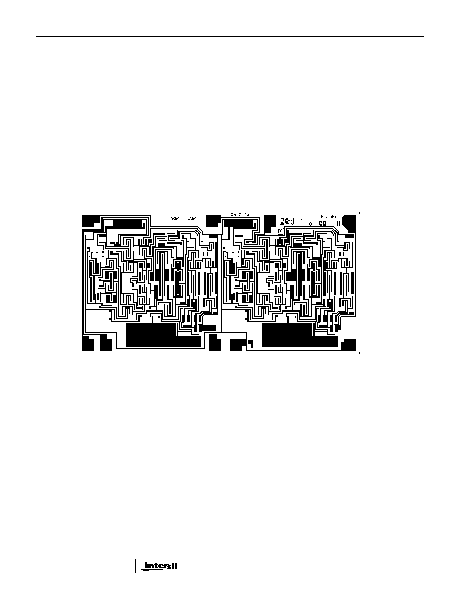
Metallization Mask Layout
HA-5142
V-
+IN1
-IN1
OUT1
+IN2
-IN2
OUT2
NC
V+
HA-5142
9
HA-5142
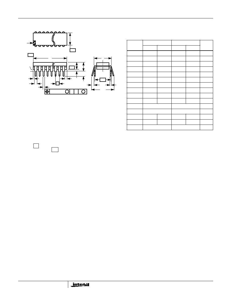
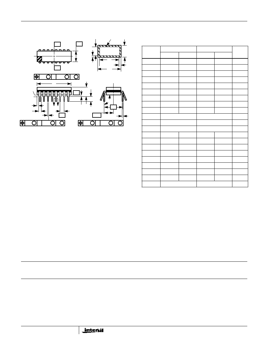
Dual-In-Line Plastic Packages (PDIP)
C
L
E
e
A
C
e
B
e
C
-B-
E1
INDEX
1 2 3
N/2
N
AREA
SEATING
BASE
PLANE
PLANE
-C-
D1
B1
B
e
D
D1
A
A2
L
A
1
-A-
0.010 (0.25)
C
A
M
B S
NOTES:
1. Controlling Dimensions: INCH. In case of conflict between
English and Metric dimensions, the inch dimensions control.
2. Dimensioning and tolerancing per ANSI Y14.5M-1982.
3. Symbols are defined in the "MO Series Symbol List" in Section
2.2 of Publication No. 95.
4. Dimensions A, A1 and L are measured with the package seated
in JEDEC seating plane gauge GS-3.
5. D, D1, and E1 dimensions do not include mold flash or protru-
sions. Mold flash or protrusions shall not exceed 0.010 inch
(0.25mm).
6. E and
are measured with the leads constrained to be per-
pendicular to datum
.
7. e
B
and e
C
are measured at the lead tips with the leads uncon-
strained. e
C
must be zero or greater.
8. B1 maximum dimensions do not include dambar protrusions.
Dambar protrusions shall not exceed 0.010 inch (0.25mm).
9. N is the maximum number of terminal positions.
10. Corner leads (1, N, N/2 and N/2 + 1) for E8.3, E16.3, E18.3,
E28.3, E42.6 will have a B1 dimension of 0.030 - 0.045 inch
(0.76 - 1.14mm).
e
A
-C-
E8.3
(JEDEC MS-001-BA ISSUE D)
8 LEAD DUAL-IN-LINE PLASTIC PACKAGE
SYMBOL
INCHES
MILLIMETERS
NOTES
MIN
MAX
MIN
MAX
A
-
0.210
-
5.33
4
A1
0.015
-
0.39
-
4
A2
0.115
0.195
2.93
4.95
-
B
0.014
0.022
0.356
0.558
-
B1
0.045
0.070
1.15
1.77
8, 10
C
0.008
0.014
0.204
0.355
-
D
0.355
0.400
9.01
10.16
5
D1
0.005
-
0.13
-
5
E
0.300
0.325
7.62
8.25
6
E1
0.240
0.280
6.10
7.11
5
e
0.100 BSC
2.54 BSC
-
e
A
0.300 BSC
7.62 BSC
6
e
B
-
0.430
-
10.92
7
L
0.115
0.150
2.93
3.81
4
N
8
8
9
Rev. 0 12/93
10
All Intersil semiconductor products are manufactured, assembled and tested under ISO9000 quality systems certification.
Intersil semiconductor products are sold by description only. Intersil Corporation reserves the right to make changes in circuit design and/or specifications at any time with-
out notice. Accordingly, the reader is cautioned to verify that data sheets are current before placing orders. Information furnished by Intersil is believed to be accurate and
reliable. However, no responsibility is assumed by Intersil or its subsidiaries for its use; nor for any infringements of patents or other rights of third parties which may result
from its use. No license is granted by implication or otherwise under any patent or patent rights of Intersil or its subsidiaries.
For information regarding Intersil Corporation and its products, see web site www.intersil.com
Sales Office Headquarters
NORTH AMERICA
Intersil Corporation
P. O. Box 883, Mail Stop 53-204
Melbourne, FL 32902
TEL: (321) 724-7000
FAX: (321) 724-7240
EUROPE
Intersil SA
Mercure Center
100, Rue de la Fusee
1130 Brussels, Belgium
TEL: (32) 2.724.2111
FAX: (32) 2.724.22.05
ASIA
Intersil (Taiwan) Ltd.
7F-6, No. 101 Fu Hsing North Road
Taipei, Taiwan
Republic of China
TEL: (886) 2 2716 9310
FAX: (886) 2 2715 3029
HA-5142
Ceramic Dual-In-Line Frit Seal Packages (CERDIP)
NOTES:
1. Index area: A notch or a pin one identification mark shall be locat-
ed adjacent to pin one and shall be located within the shaded
area shown. The manufacturer's identification shall not be used
as a pin one identification mark.
2. The maximum limits of lead dimensions b and c or M shall be
measured at the centroid of the finished lead surfaces, when
solder dip or tin plate lead finish is applied.
3. Dimensions b1 and c1 apply to lead base metal only. Dimension
M applies to lead plating and finish thickness.
4. Corner leads (1, N, N/2, and N/2+1) may be configured with a
partial lead paddle. For this configuration dimension b3 replaces
dimension b2.
5. This dimension allows for off-center lid, meniscus, and glass
overrun.
6. Dimension Q shall be measured from the seating plane to the
base plane.
7. Measure dimension S1 at all four corners.
8. N is the maximum number of terminal positions.
9. Dimensioning and tolerancing per ANSI Y14.5M - 1982.
10. Controlling dimension: INCH
bbb
C A - B
S
c
Q
L
A
SEATING
BASE
D
PLANE
PLANE
-D-
-A-
-C-
-B-
D
E
S1
b2
b
A
e
M
c1
b1
(c)
(b)
SECTION A-A
BASE
LEAD FINISH
METAL
e
A/2
A
M
S
S
ccc
C A - B
M
D
S
S
aaa
C A - B
M
D
S
S
e
A
F8.3A
MIL-STD-1835 GDIP1-T8 (D-4, CONFIGURATION A)
8 LEAD CERAMIC DUAL-IN-LINE FRIT SEAL PACKAGE
SYMBOL
INCHES
MILLIMETERS
NOTES
MIN
MAX
MIN
MAX
A
-
0.200
-
5.08
-
b
0.014
0.026
0.36
0.66
2
b1
0.014
0.023
0.36
0.58
3
b2
0.045
0.065
1.14
1.65
-
b3
0.023
0.045
0.58
1.14
4
c
0.008
0.018
0.20
0.46
2
c1
0.008
0.015
0.20
0.38
3
D
-
0.405
-
10.29
5
E
0.220
0.310
5.59
7.87
5
e
0.100 BSC
2.54 BSC
-
eA
0.300 BSC
7.62 BSC
-
eA/2
0.150 BSC
3.81 BSC
-
L
0.125
0.200
3.18
5.08
-
Q
0.015
0.060
0.38
1.52
6
S1
0.005
-
0.13
-
7
90
o
105
o
90
o
105
o
-
aaa
-
0.015
-
0.38
-
bbb
-
0.030
-
0.76
-
ccc
-
0.010
-
0.25
-
M
-
0.0015
-
0.038
2, 3
N
8
8
8
Rev. 0 4/94