3-94
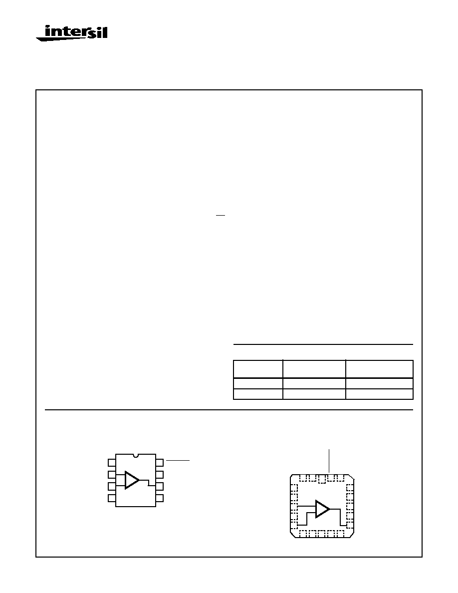
Pinouts
HA-5020/883
(CERDIP)
TOP VIEW
HA-5020/883
(CLCC)
TOP VIEW
BAL
-IN
+IN
V-
1
2
3
4
8
7
6
5
DISABLE
V+
OUT
BAL
+
-
4
5
6
7
8
9
10 11 12 13
3
2
1
19
15
14
18
17
16
NC
NC
-IN
NC
+IN
NC
NC
NC
OUT
V+
DISABLE
NC
NC
V-
NC
BA
L
NC
NC
BA
L
NC
20
+
-
HA-5020/883
100MHz Current Feedback
Video Amplifier with Disable
Description
The HA-5020/883 is a wide bandwidth, high slew rate
amplifier optimized for video applications and gains between
1 and 10. Manufactured on Intersil's Reduced Feature
Complementary Bipolar DI process, this amplifier uses cur-
rent mode feedback to maintain higher bandwidth at a given
gain than conventional voltage feedback amplifiers. Since it
is a closed loop device, the HA-5020/883 offers better gain
accuracy and lower distortion than open loop buffers.
The HA-5020/883 features low differential gain and phase and
will drive two double terminated 75
coax cables to video
levels with low distortion. Adding a gain flatness performance
of 0.1dB makes this amplifier ideal for demanding video
applications. The bandwidth and slew rate of the HA-5020/
883 are relatively independent of closed loop gain. The
105MHz unity gain bandwidth only decreases to 77MHz at a
gain of 10. The HA-5020/883 used in place of a conventional
op amp will yield a significant improvement in the speed
power product. To further reduce power, the HA-5020/883 has
a disable function which significantly reduces supply current,
while forcing the output to a true high impedance state. This
allows the outputs of multiple amplifiers to be wire-OR'd into
multiplexer configurations. The device also includes output
short circuit protection and output offset voltage adjustment.
The HA-5020/883 offers significant enhancements over
competing amplifiers, such as the EL2020. Improvements
include unity gain bandwidth, slew rate, video performance,
lower supply current, and superior DC specifications.
Ordering Information
PART
NUMBER
TEMPERATURE
RANGE
PACKAGE
HA7-5020/883
-55
o
C to +125
o
C
8 Lead CerDIP
HA4-5020/883
-55
o
C to +125
o
C
20 Lead Ceramic LCC
Features
� This Circuit is Processed in Accordance to MIL-STD-
883 and is Fully Conformant Under the Provisions of
Paragraph 1.2.1.
� Wide Unity Gain Bandwidth . . . . . . . . . . 105MHz (Min)
� Slew Rate . . . . . . . . . . . . . . . . . . . . . . . . . . . . . . 800V/
�
s
� Output Current . . . . . . . . . . . . . . . . . . . . . .
�
30mA (Min)
� Drives 3.5V into 75
� Differential Gain . . . . . . . . . . . . . . . . . . . . . . . . . . 0.025%
� Differential Phase. . . . . . . . . . . . . . . . . . . . . . .0.025 Deg
� Low Input Noise Voltage . . . . . . . . . . . . . . . . 4.5nV/
Hz
� Low Supply Current . . . . . . . . . . . . . . . . . . . 10mA (Max)
� Wide Supply Range . . . . . . . . . . . . . . . . . . .
�
5V to
�
15V
� Output Enable/Disable
� High Performance Replacement for EL2020/883
Applications
� Unity Gain Video/Wideband Buffer
� Video Gain Block
� Video Distribution Amp/Coax Cable Driver
� Flash A/D Driver
� Waveform Generator Output Driver
� Current to Voltage Converter; D/A Output Buffer
� Radar Systems
� Imaging Systems
January 1996
Spec Number
511080-883
File Number
3541.2
CAUTION: These devices are sensitive to electrostatic discharge; follow proper IC Handling Procedures.
1-888-INTERSIL or 321-724-7143
|
Copyright
�
Intersil Corporation 1999
3-95
Specifications HA-5020/883
Absolute Maximum Ratings
Thermal Information (Typical)
Voltage Between V+ and V- Terminals . . . . . . . . . . . . . . . . . . . . 36V
Differential Input Voltage. . . . . . . . . . . . . . . . . . . . . . . . . . . . . . . . 8V
Voltage at Either Input Terminal . . . . . . . . . . . . . . . . . . . . . . V+ to V-
Peak Output Current. . . . . . . . . . . . . . . . Full Short Circuit Protected
Junction Temperature (T
J
) . . . . . . . . . . . . . . . . . . . . . . . . . . +175
o
C
Storage Temperature Range . . . . . . . . . . . . . . . . . -65
o
C to +150
o
C
ESD Rating. . . . . . . . . . . . . . . . . . . . . . . . . . . . . . . . . . . . . . < 2000V
Lead Temperature (Soldering 10s) . . . . . . . . . . . . . . . . . . . . +300
o
C
Thermal Package Characteristics
JA
JC
CerDIP Package . . . . . . . . . . . . . . . . . . . . . . 115
o
C/W
30
o
C/W
Ceramic LCC Package . . . . . . . . . . . . . . . . . 75
o
C/W
23
o
C/W
Package Power Dissipation Limit at +75
o
C for T
J
+175
o
C
CerDIP Package . . . . . . . . . . . . . . . . . . . . . . . . . . . . . . . . . 0.87W
Ceramic LCC Package . . . . . . . . . . . . . . . . . . . . . . . . . . . . 1.33W
Package Power Dissipation Derating Factor Above +75
o
C
CerDIP Package . . . . . . . . . . . . . . . . . . . . . . . . . . . . . . 8.7mW/
o
C
Ceramic LCC Package . . . . . . . . . . . . . . . . . . . . . . . . 13.3mW/
o
C
CAUTION: Stresses above those listed in "Absolute Maximum Ratings" may cause permanent damage to the device. This is a stress only rating and operation
of the device at these or any other conditions above those indicated in the operational sections of this specification is not implied.
Operating Conditions
Operating Temperature Range . . . . . . . . . . . . . . . . -55
o
C to +125
o
C
Operating Supply Voltage
. . . . . . . . . . . . . . . . . . . . . . . . . . �
5V to
�
15V
V
INCM
1/2(V+ - V-)
R
F
= 1k
R
L
400
V
DISABLE
= V+ or 0V
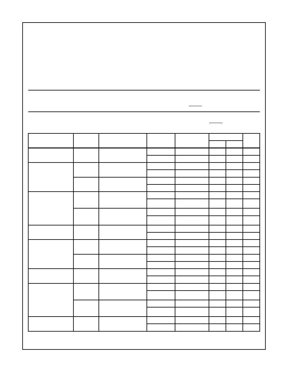
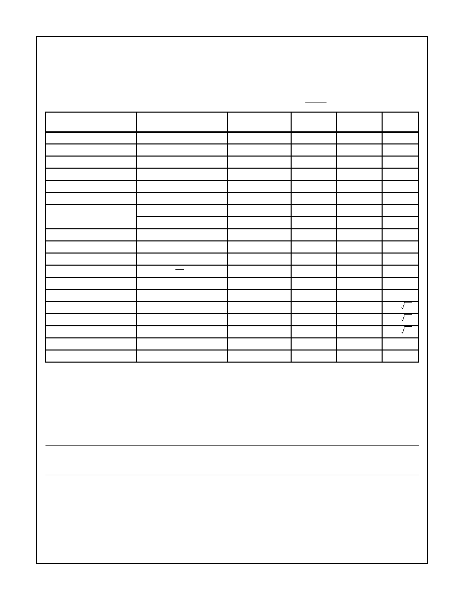
TABLE 1. DC ELECTRICAL PERFORMANCE CHARACTERISTICS
Device Tested at: Supply Voltage =
�
15V, R
SOURCE
= 0
, A
VCL
= +1, R
F
= 1k
, R
LOAD
= 400
, V
OUT
= 0V, V
DISABLE
= V+,
Unless Otherwise Specified.
PARAMETERS
SYMBOL
CONDITIONS
GROUP A
SUBGROUP
TEMPERATURE
LIMITS
UNITS
MIN
MAX
Input Offset Voltage
V
IO
V
CM
= 0V
1
+25
o
C
-8
8
mV
2, 3
+125
o
C, -55
o
C
-10
10
mV
Common Mode
Rejection Ratio
+CMRR
V
CM
= +10V, V+ = 5V,
V- = -25V
1
+25
o
C
60
-
dB
2, 3
+125
o
C, -55
o
C
50
-
dB
-CMRR
V
CM
= -10V, V+ = 25V,
V- = -5V
1
+25
o
C
60
-
dB
2, 3
+125
o
C, -55
o
C
50
-
dB
Power Supply Rejection
Ratio
+PSRR
V
SUP
= 13.5V,
V+ = 4.5V, V- = -15V;
V+ = 18V, V- = -15V
1
+25
o
C
64
-
dB
2, 3
+125
o
C, -55
o
C
60
-
dB
-PSRR
V
SUP
= 13.5V,
V+ = 15V, V- = -4.5V;
V+ = 15V, V- = -18V
1
+25
o
C
64
-
dB
2, 3
+125
o
C, -55
o
C
60
-
dB
Non-Inverting (+IN)
Current
I
BP
V
CM
= 0V
1
+25
o
C
-8
8
�
A
2, 3
+125
o
C, -55
o
C
-20
20
�
A
+IN Common Mode
Rejection
IBPCMP
V
CM
= +10V, V+ = 5V,
V- = -25V
1
+25
o
C
-
0.1
�
A/V
2, 3
+125
o
C, -55
o
C
-
0.5
�
A/V
IBPCMN
V
CM
= -10V, V+ = 25V,
V- = -5V
1
+25
o
C
-
0.1
�
A/V
2, 3
+125
o
C, -55
o
C
-
0.5
�
A/V
Non-Inverting (+IN) Input
Impedance
+R
IN
Calculated 1/IBPCMP
1
+25
o
C
10
-
M
2, 3
+125
o
C, -55
o
C
2
-
M
+IN Power Supply
Rejection
IBPPSP
V
SUP
= 13.5V,
V+ = 4.5V, V- = -15V;
V+ = 18V, V- = -15V
1
+25
o
C
-
0.06
�
A/V
2, 3
+125
o
C, -55
o
C
-
0.2
�
A/V
IBPPSN
V
SUP
= 13.5V,
V+ = 15V, V- = -4.5V;
V+ = 15V, V- = -18V
1
+25
o
C
-
0.06
�
A/V
2, 3
+125
o
C, -55
o
C
-
0.2
�
A/V
Inverting Input (-IN)
Current
I
BN
V
CM
= 0V
1
+25
o
C
-20
20
�
A
2, 3
+125
o
C, -55
o
C
-50
50
�
A
Spec Number
511080-883
3-96
Specifications HA-5020/883
-IN Common Mode
Rejection
IBNCMP
V
CM
= +10V, V+ = 5V,
V- = -25V
1
+25
o
C
-
0.4
�
A/V
2, 3
+125
o
C, -55
o
C
-
0.5
�
A/V
IBNCMN
V
CM
= -10V, V+ = 25V,
V- = -5V
1
+25
o
C
-
0.4
�
A/V
2, 3
+125
o
C, -55
o
C
-
0.5
�
A/V
-IN Power Supply
Rejection
IBNPSP
V
SUP
= 13.5V,
V+ = 4.5V, V- = -15V;
V+ = 18V, V- = -15V
1
+25
o
C
-
0.2
�
A/V
2, 3
+125
o
C, -55
o
C
-
0.5
�
A/V
IBNPSN
V
SUP
= 13.5V,
V+ = 15V, V- = -4.5V;
V+ = 15V, V- = -18V
1
+25
o
C
-
0.2
�
A/V
2, 3
+125
o
C, -55
o
C
-
0.5
�
A/V
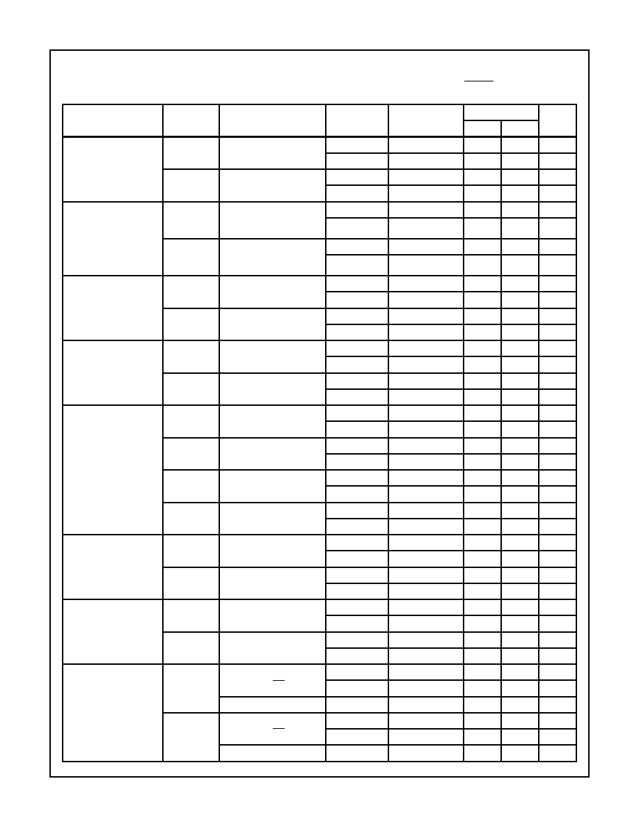
Common Mode Range
+CMR
V+ = 5V, V- = -25V
1
+25
o
C
10
-
V
2, 3
+125
o
C, -55
o
C
10
-
V
-CMR
V+ = 25V, V- = -5V
1
+25
o
C
-
-10
V
2, 3
+125
o
C, -55
o
C
-
-10
V
Transimpedance
+A
ZOL1
R
L
= 400
, V
OUT
= 0 to
10V
1
+25
o
C
1
-
M
2, 3
+125
o
C, -55
o
C
1
-
M
-A
ZOL1
R
L
= 400
, V
OUT
= 0 to
-10V
1
+25
o
C
1
-
M
2, 3
+125
o
C, -55
o
C
1
-
M
Output Voltage Swing
+V
OUT
V
IN
= 12.8V
1, 2
+25
o
C, +125
o
C
12
-
V
3
-55
o
C
11
-
V
-V
OUT
V
IN
= -12.8V
1, 2
+25
o
C, +125
o
C
-
-12
V
3
-55
o
C
-
-11
V
+V
OUT5
V+ = 5V, V- = -5V,
V
IN
= 3V
1
+25
o
C
2
-
V
2, 3
+125
o
C, -55
o
C
2
-
V
-V
OUT5
V+ = 5V, V- = -5V,
V
IN
= -3V
1
+25
o
C
-
-2
V
2, 3
+125
o
C, -55
o
C
-
-2
V
Output Current
+I
OUT
Note 1
1, 2
+25
o
C, +125
o
C
30
-
mA
3
-55
o
C
27.5
-
mA
-I
OUT
Note 1
1, 2
+25
o
C, +125
o
C
-
-30
mA
3
-55
o
C
-
-27.5
mA
Short Circuit Output
Current
+I
SC
R
L
= Open, V
IN
= 10V
1
+25
o
C
50
-
mA
2, 3
+125
o
C, -55
o
C
50
-
mA
-I
SC
R
L
= Open, V
IN
= -10V
1
+25
o
C
-
-50
mA
2, 3
+125
o
C, -55
o
C
-
-50
mA
Disabled Output Current
+I
LEAK
V
IN
= 0V, V
OUT
= +10V,
R
L
= Open, V
DIS
= 0V
1
+25
o
C
-1
1
�
A
3
-55
o
C
-1
1
�
A
V
IN
= 2V
2
+125
o
C
-1
1
�
A
-I
LEAK
V
IN
= 0V, V
OUT
= -10V,
R
L
= Open, V
DIS
= 0V
1
+25
o
C
-1
1
�
A
3
-55
o
C
-1
1
�
A
V
IN
= -2V
2
+125
o
C
-1
1
�
A
TABLE 1. DC ELECTRICAL PERFORMANCE CHARACTERISTICS
(Continued)
Device Tested at: Supply Voltage =
�
15V, R
SOURCE
= 0
, A
VCL
= +1, R
F
= 1k
, R
LOAD
= 400
, V
OUT
= 0V, V
DISABLE
= V+,
Unless Otherwise Specified.
PARAMETERS
SYMBOL
CONDITIONS
GROUP A
SUBGROUP
TEMPERATURE
LIMITS
UNITS
MIN
MAX
Spec Number
511080-883
3-97
Specifications HA-5020/883
Disable Pin Input Current
I
LOGIC
V
DIS
= 0V
1, 2
+25
o
C, +125
o
C
-1
0
mA
3
-55
o
C
-1.5
0
mA
Minimum DISABLE Pin
Current to Disable
I
DIS
Note 2
1
+25
o
C
-
350
�
A
2, 3
+125
o
C, -55
o
C
-
350
�
A
Maximum DISABLE Pin
Current to Enable
I
EN
Note 3
1
+25
o
C
20
-
�
A
2, 3
+125
o
C, -55
o
C
20
-
�
A
Quiescent Power Supply
Current
I
CC
R
L
= 400
1
+25
o
C
-
10
mA
2, 3
+125
o
C, -55
o
C
-
10
mA
I
EE
R
L
= 400
1
+25
o
C
-10
-
mA
2, 3
+125
o
C, -55
o
C
-10
-
mA
Disabled Power Supply
Current
I
CCDIS
R
L
= 400
, V
DIS
= 0V
1
+25
o
C
-
5.6
mA
2, 3
+125
o
C, -55
o
C
-
7.5
mA
I
EEDIS
R
L
= 400
, V
DIS
= 0V
1
+25
o
C
-5.6
-
mA
2, 3
+125
o
C, -55
o
C
-7.5
-
mA
Offset Voltage
Adjustment
+V
ADJ
Note 4
1
+25
o
C
30
-
mV
2, 3
+125
o
C, -55
o
C
25
-
mV
-V
ADJ
Note 4
1
+25
o
C
-
-30
mV
2, 3
+125
o
C, -55
o
C
-
-25
mV
NOTES:
1. Guaranteed from V
OUT
test by I
OUT
= V
OUT
/400
.
2. This is the minimum current which must be sourced from the DISABLE pin, to disable the output. The output is considered disabled when
V
OUT
10mV. Conditions are: V
IN
= 10V, R
L
= 100
. The test is performed by sourcing 350
�
A from the DISABLE pin, and testing that
the output decreases below the test limit (10mV).
3. This is the maximum current that can be sourced from the DISABLE pin with the device remaining enabled. The device is considered
disabled when the supply current decreases by at least 0.5mA. Conditions are: R
L
= 400
. Test is performed by sourcing 20
�
A from the
DISABLE pin, and testing that the supply current decreases by no more than the test limit (0.5mA).
4. The offset adjustment range is referred to the output. The inverting input current (-I
BIAS
) can be adjusted with an external pot between pins
1 and 5, wiper connected to V+. Since -I
BIAS
flows through R
F
, an adjustment of offset voltage results. The amount of offset adjustment is
proportional to the value of R
F
. Test conditions are: R
L
= Open, 10k
from pin 5 to V+, 1k
from pin 1 to V+, for +V
ADJ
; R
L
= Open, 1k
from pin 5 to V+, 10k
from pin 1 to V+, for -V
ADJ
.
TABLE 2. AC ELECTRICAL PERFORMANCE CHARACTERISTICS
Device Tested at: Supply Voltage =
�
15V, R
SOURCE
= 50
, R
LOAD
= 400
, C
LOAD
10pF, A
VCL
= +1V/V, Unless Otherwise Specified.
PARAMETERS
SYMBOL
CONDITIONS
GROUP A
SUBGROUP
TEMPERATURE
LIMITS
UNITS
MIN
MAX
Slew Rate
+SR
V
IN
= -10V to +10V
4
+25
o
C
600
-
V/
�
s
5, 6
+125
o
C, -55
o
C
400
-
V/
�
s
-SR
V
IN
= +10V to -10V
4
+25
o
C
600
-
V/
�
s
5, 6
+125
o
C, -55
o
C
400
-
V/
�
s
TABLE 1. DC ELECTRICAL PERFORMANCE CHARACTERISTICS
(Continued)
Device Tested at: Supply Voltage =
�
15V, R
SOURCE
= 0
, A
VCL
= +1, R
F
= 1k
, R
LOAD
= 400
, V
OUT
= 0V, V
DISABLE
= V+,
Unless Otherwise Specified.
PARAMETERS
SYMBOL
CONDITIONS
GROUP A
SUBGROUP
TEMPERATURE
LIMITS
UNITS
MIN
MAX
Spec Number
511080-883
3-98
Specifications HA-5020/883
TABLE 3. ELECTRICAL PERFORMANCE CHARACTERISTICS
Device Characterized at: Supply Voltage =
�
15V, R
SOURCE
= 50
, R
LOAD
= 400
, R
F
= 1k
, V
DISABLE
= V+, C
LOAD
10pF, A
VCL
= +1V/V,
Unless Otherwise Specified.
PARAMETERS
SYMBOL
CONDITIONS
NOTES
TEMPERATURE
LIMITS
UNITS
MIN
MAX
-3dB Bandwidth
BW
1
V
O
= 100mV
RMS
, A
V
= +1
1
+25
o
C
105
-
MHz
BW
10
V
O
= 100mV
RMS
, A
V
= +10,
R
F
= 360
, R
L
= Open
1
+25
o
C
77
-
MHz
Gain Flatness
GF
5
V
O
= 100mV
RMS
, f = 5MHz
1
+25
o
C
-0.075
+0.075
dB
GF
10
V
O
= 100mV
RMS
, f = 10MHz
1
+25
o
C
-0.2
+0.2
dB
Rise Time
t
R
V
O
= 0V to 1V, R
L
= 100
1, 2
+25
o
C
-
3.7
ns
Fall Time
t
F
V
O
= 1V to 0V, R
L
= 100
1, 3
+25
o
C
-
4.0
ns
Overshoot
+OVS
V
O
= 0V to 1V, R
L
= 100
1
+25
o
C
-
18.0
%
-OVS
V
O
= 1V to 0V, R
L
= 100
1
+25
o
C
-
16.6
%
Slew Rate
+SR
10
V
O
= -10V to 10V, A
V
= +10,
R
F
= 360
, R
L
= Open
1, 4
+25
o
C
1070
-
V/
�
s
-SR
10
V
O
= 10V to -10V, A
V
= +10,
R
F
= 360
, R
L
= Open
1, 5
+25
o
C
860
-
V/
�
s
Disable Time
+t
DIS
V
O
= 2V to 0V, 50% of V
DIS
to
90% V
O
1, 6
+25
o
C
-
3.13
�
s
-t
DIS
V
O
= -2V to 0V, 50% of V
DIS
to
90% V
O
1, 6
+25
o
C
-
2.44
�
s
Enable Time
+t
EN
V
O
= 0V to 2V, 50% to 90%
1, 7
+25
o
C
-
1.45
�
s
-t
EN
V
O
= 0V to -2V, 50% to 90%
1, 7
+25
o
C
-
1.49
�
s
NOTES:
1. Parameters listed in Table 3 are controlled via design or process parameters and are not directly tested at final production. These param-
eters are lab characterized upon initial design release, or upon design changes. These parameters are guaranteed by characterization
based upon data from multiple production runs which reflect lot to lot and within lot variation.
2. Measured from 10% to 90% of the output waveform.
3. Measured from 90% to 10% of the output waveform.
4. Measured from 25% to 75% of the output waveform.
5. Measured from 75% to 25% of the output waveform.
6. DISABLE = +15V to 0V. Measured from the 50% of DISABLE to V
OUT
=
�
200mV.
7. DISABLE = 0V to +15V. Measured from the 50% of DISABLE to V
OUT
=
�
1.8V.
TABLE 4. ELECTRICAL TEST REQUIREMENTS
MIL-STD-883 TEST REQUIREMENTS
SUBGROUPS (SEE TABLES 1 AND 2)
Interim Electrical Parameters (Pre Burn-In)
1
Final Electrical Test Parameters
1 (Note 1), 2, 3, 4, 5, 6
Group A Test Requirements
1, 2, 3, 4, 5, 6
Groups C and D Endpoints
1
NOTE:
1. PDA applies to Subgroup 1 only.
Spec Number
511080-883
3-99
HA-5020/883
Die Characteristics
DIE DIMENSIONS:
65 x 60 x 19 mils
�
1 mils
1640
�
m x 1520
�
m x 483
�
m
�
25.4
�
m
METALLIZATION:
Type: Al, 1% Cu
Thickness: 16k
�
�
2k
�
WORST CASE CURRENT DENSITY:
5.77 x 10
4
A/cm
2
at 30mA
SUBSTRATE POTENTIAL (Powered Up): V-
GLASSIVATION:
Type: Nitride over Silox
Silox Thickness: 12k
�
�
2k
�
Nitride Thickness: 3.5k
�
�
1k
�
TRANSISTOR COUNT: 62
PROCESS: Bipolar Dielectric Isolation
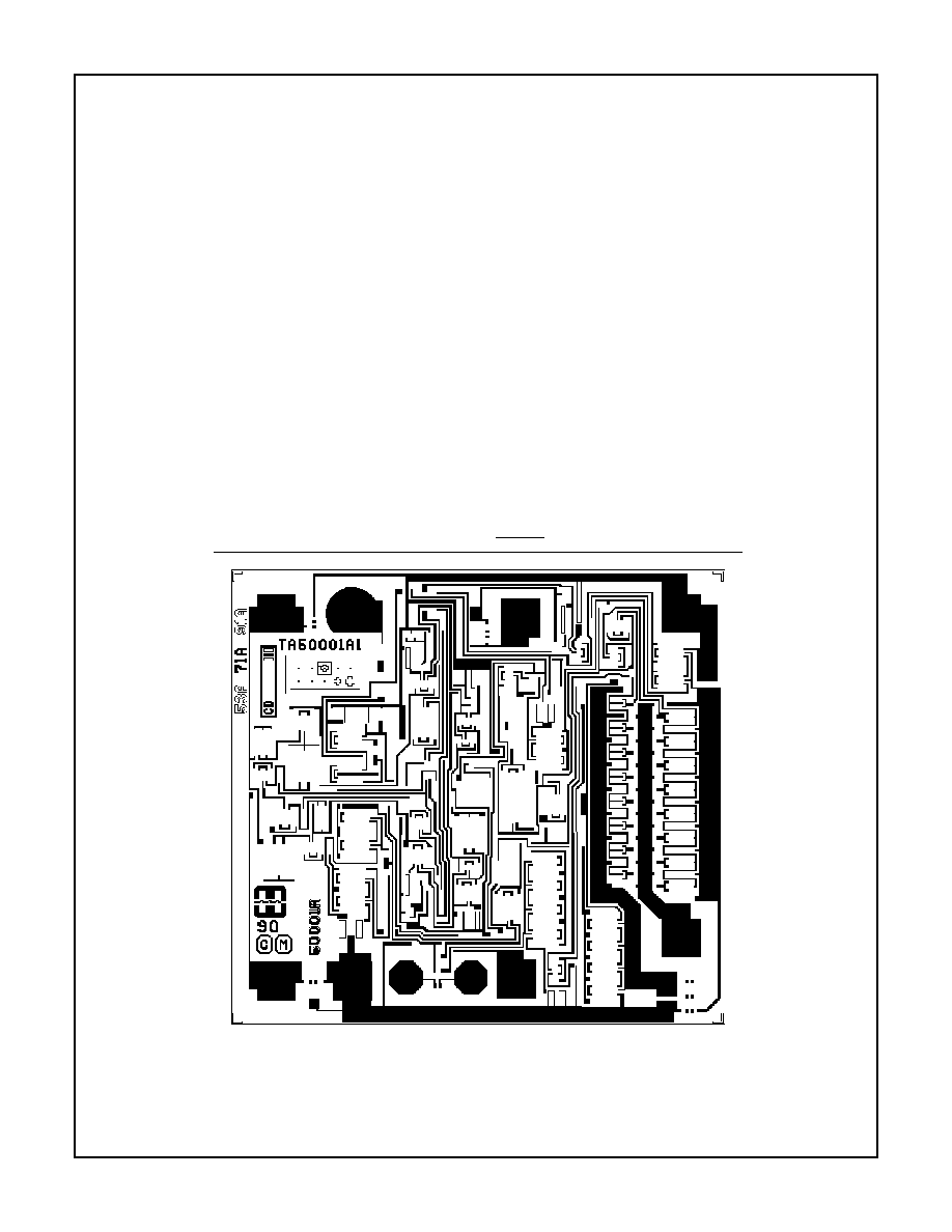
Metallization Mask Layout
HA-5020/883
4
3
2
1
8
7
6
5
+IN
-IN
BAL
DISABLE
V+
OUT
BAL
V-
Spec Number
511080-883

3-100
HA-5020/883
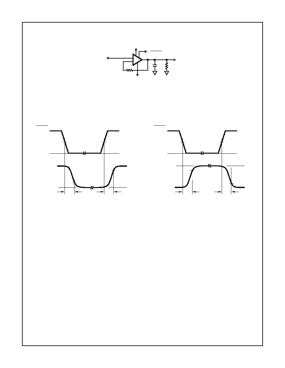
Test Circuit
(Applies to Table 1)
Test Waveforms
SIMPLIFIED TEST CIRCUIT FOR LARGE AND SMALL SIGNAL PULSE RESPONSE (Applies to Tables 2 and 3)
A
V
= +1 TEST CIRCUIT
A
V
= +10 TEST CIRCUIT
LARGE SIGNAL WAVEFORM
SMALL SIGNAL WAVEFORM
V+
ICC
10
0.1
1K
10K
1K
10K
K9
K10
BAL. ADJ.
7
1
5
DUT
-
+
2
3
4
8
1K
(0.01%)
150pF
500
500
V
IN
-
+
HA-5177
200pF
200K (0.1%)
V
Z
K7
V
X
x100
-
+
0.1
VIO =
V
X
100
+I
BIAS
=
V
Z
200K
10
0.1
V-
IEE
V
DISABLE
500
-
+
V
Y
-I
BIAS
=
V
Y
100K
K3
K4
K1
1K
400
100
K12
V
OUT
NOTE: All Resistors =
�
1% (
)
All Capacitors =
�
10% (
�
F)
Unless Otherwise Noted
0.1
x100
6
-
+
V
IN
R
S
50
C
L
R
L
V
OUT
V+
V
DISABLE
R
L
1k
V-
NOTE: V
S
=
�
15V, A
V
= +1, C
L
10pF
R
F
= 1k
, R
S
= 50
R
L
= 400
For Large Signal
R
L
= 100
For Small Signal
-
+
V
IN
R
S
50
R
F
V
OUT
V+
V
DISABLE
V-
360
R
G
40
NOTE: V
S
=
�
15V, A
V
= +10, C
L
10pF
R
F
= 360
, R
G
= 40
R
S
= 50
,
R
L
= Open
75%
25%
75%
25%
+10V
-SR, -SR10
+10V
+SR, +SR10
V
OUT
-10V
-10V
NOTE: A
V
= +1: +SR, -SR
A
V
= +10: +SR10, -SR10
90%
10%
90%
10%
+1V
tf, -OVS
+1V
tr, +OVS
V
OUT
0V
0V
Spec Number
511080-883
3-101
HA-5020/883
SIMPLIFIED TEST CIRCUIT FOR ENABLE/DISABLE TIMES
POSITIVE ENABLE/DISABLE SWITCHING WAVEFORMS
NEGATIVE ENABLE/DISABLE SWITCHING WAVEFORMS
Test Waveforms
(Continued)
-
+
V
IN
C
L
R
L
V
OUT
V+
V
DISABLE
R
F
1k
V-
NOTE: V
S
=
�
15V, A
V
= +1, C
L
10pF
R
F
= 1k
, R
L
= 400
50%
50%
+15V
+15V
V
DISABLE
0V
0V
10%
+tDIS
+tEN
+2V
+2V
0V
0V
90%
VOUT
50%
50%
+15V
+15V
V
DISABLE
0V
0V
90%
-tDIS
-tEN
-2V
-2V
0V
0V
10%
VOUT
Spec Number
511080-883
3-102
HA-5020/883
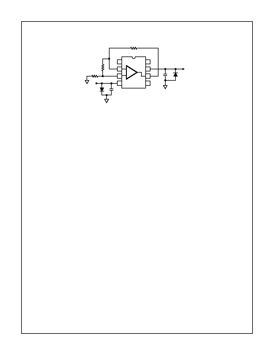
Burn-In Circuits
HA7-5020/883 CERAMIC DIP
1
2
3
4
8
7
6
5
+
-
V+
C1
D1
R3
R1
R2
D2
C2
V-
Spec Number
511080-883
3-103
HA-5020/883
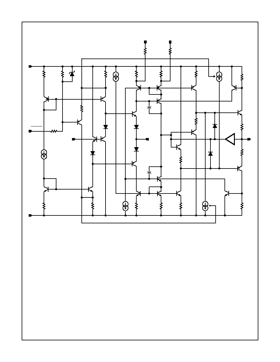
Schematic Diagram
OUT
+1
BAL
BAL
-IN
5Ibp
5Ibn
+IN
I
REF
V+
V
DISABLE
V-
Spec Number
511080-883
3-104
HA-5020/883
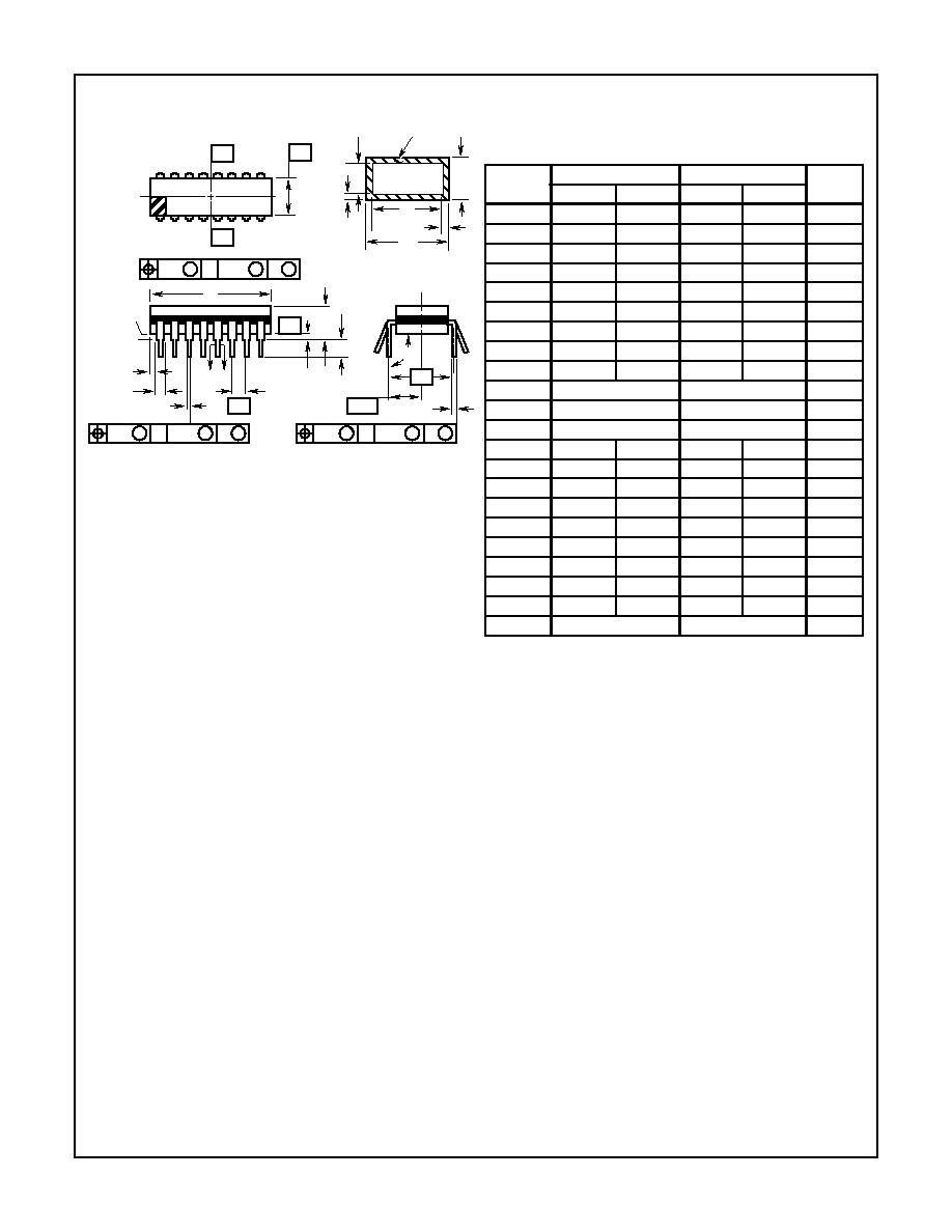
F8.3A
MIL-STD-1835 GDIP1-T8 (D-4, CONFIGURATION A)
8 LEAD DUAL-IN-LINE FRIT-SEAL CERAMIC PACKAGE
SYMBOL
INCHES
MILLIMETERS
NOTES
MIN
MAX
MIN
MAX
A
-
0.200
-
5.08
-
b
0.014
0.026
0.36
0.66
2
b1
0.014
0.023
0.36
0.58
3
b2
0.045
0.065
1.14
1.65
-
b3
0.023
0.045
0.58
1.14
4
c
0.008
0.018
0.20
0.46
2
c1
0.008
0.015
0.20
0.38
3
D
-
0.405
-
10.29
5
E
0.220
0.310
5.59
7.87
5
e
0.100 BSC
2.54 BSC
-
eA
0.300 BSC
7.62 BSC
-
eA/2
0.150 BSC
3.81 BSC
-
L
0.125
0.200
3.18
5.08
-
Q
0.015
0.060
0.38
1.52
6
S1
0.005
-
0.13
-
7
S2
0.005
-
0.13
-
-
90
o
105
o
90
o
105
o
-
aaa
-
0.015
-
0.38
-
bbb
-
0.030
-
0.76
-
ccc
-
0.010
-
0.25
-
M
-
0.0015
-
0.038
2
N
8
8
8
Packaging
NOTES:
1. Index area: A notch or a pin one identification mark shall be locat-
ed adjacent to pin one and shall be located within the shaded
area shown. The manufacturer's identification shall not be used
as a pin one identification mark.
2. The maximum limits of lead dimensions b and c or M shall be
measured at the centroid of the finished lead surfaces, when
solder dip or tin plate lead finish is applied.
3. Dimensions b1 and c1 apply to lead base metal only. Dimension
M applies to lead plating and finish thickness.
4. Corner leads (1, N, N/2, and N/2+1) may be configured with a
partial lead paddle. For this configuration dimension b3 replaces
dimension b1.
5. This dimension allows for off-center lid, meniscus, and glass
overrun.
6. Dimension Q shall be measured from the seating plane to the
base plane.
7. Measure dimension S1 at all four corners.
8. N is the maximum number of terminal positions.
9. Dimensioning and tolerancing per ANSI Y14.5M - 1982.
10. Controlling Dimension: Inch.
11. Lead Finish: Type A.
12. Materials: Compliant to MIL-M-38510.
bbb
C A - B
S
c
Q
L
A
SEATING
BASE
D
PLANE
PLANE
-D-
-A-
-C-
-B-
D
E
S1
b2
b
A
e
M
c1
b1
(c)
(b)
SECTION A-A
BASE
LEAD FINISH
METAL
e
A/2
A
M
S
S
e
A
ccc
C A - B
M
D
S
S
aaa
C A - B
M
D
S
S
Spec Number
511080-883
3-105
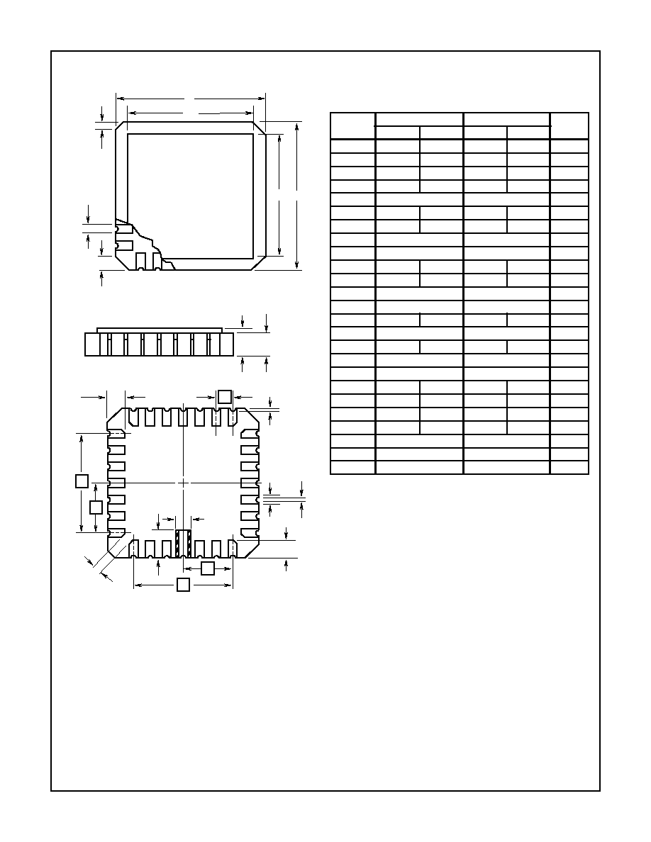
HA-5020/883
Packaging
(Continued)
D
j x 45
o
D3
B
h x 45
o
A
A1
E
L
L3
e
B3
B1
L1
D2
D1
e
1
E2
E1
L2
PLANE 2
PLANE 1
E3
B2
NOTES:
1. Metallized castellations shall be connected to plane 1 terminals
and extend toward plane 2 across at least two layers of ceramic
or completely across all of the ceramic layers to make electrical
connection with the optional plane 2 terminals.
2. Unless otherwise specified, a minimum clearance of 0.015 inch
(0.381mm) shall be maintained between all metallized features
(e.g., lid, castellations, terminals, thermal pads, etc.)
3. Symbol "N" is the maximum number of terminals. Symbols "ND"
and "NE" are the number of terminals along the sides of length
"D" and "E", respectively.
4. The required plane 1 terminals and optional plane 2 terminals
shall be electrically connected.
5. The corner shape (square, notch, radius, etc.) may vary at the
manufacturer's option, from that shown on the drawing.
6. Chip carriers shall be constructed of a minimum of two ceramic
layers.
7. Maximum limits allows for 0.007 inch solder thickness on pads.
8. Lead Finish: Type A.
9. Materials: Compliant to MIL-M-38510.
J20.A
MIL-STD-1835 CQCC1-N20 (C-2)
20 PAD METAL SEAL LEADLESS CERAMIC CHIP CARRIER
SYMBOL
INCHES
MILLIMETERS
NOTES
MIN
MAX
MIN
MAX
A
0.060
0.100
1.52
2.54
6, 7
A1
0.050
0.088
1.27
2.23
7
B
-
-
-
-
4
B1
0.022
0.028
0.56
0.71
2, 4
B2
0.072 REF
1.83 REF
-
B3
0.006
0.022
0.15
0.56
-
D
0.342
0.358
8.69
9.09
-
D1
0.200 BSC
5.08 BSC
-
D2
0.100 BSC
2.54 BSC
-
D3
-
0.358
-
9.09
2
E
0.342
0.358
8.69
9.09
-
E1
0.200 BSC
5.08 BSC
-
E2
0.100 BSC
2.54 BSC
-
E3
-
0.358
-
9.09
2
e
0.050 BSC
1.27 BSC
-
e1
0.015
-
0.38
-
2
h
0.040 REF
1.02 REF
5
j
0.020 REF
0.51 REF
5
L
0.045
0.055
1.14
1.40
-
L1
0.045
0.055
1.14
1.40
-
L2
0.075
0.095
1.90
2.41
-
L3
0.003
0.015
0.08
0.38
-
ND
5
5
3
NE
5
5
3
N
20
20
3
Spec Number
511080-883
The information contained in this section has been developed through characterization by Harris Semiconductor and is for use as application
and design information only. No guarantee is implied.
3-106
DESIGN INFORMATION
December 1999
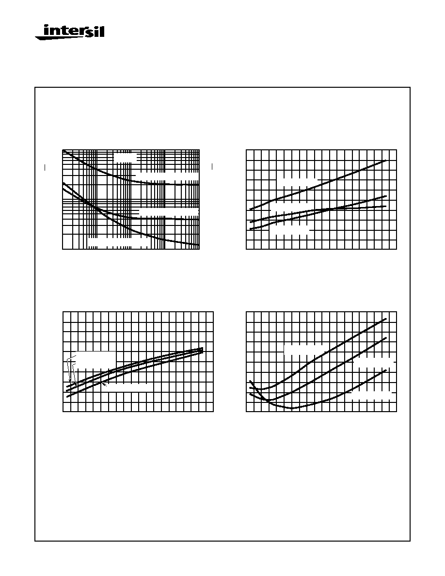
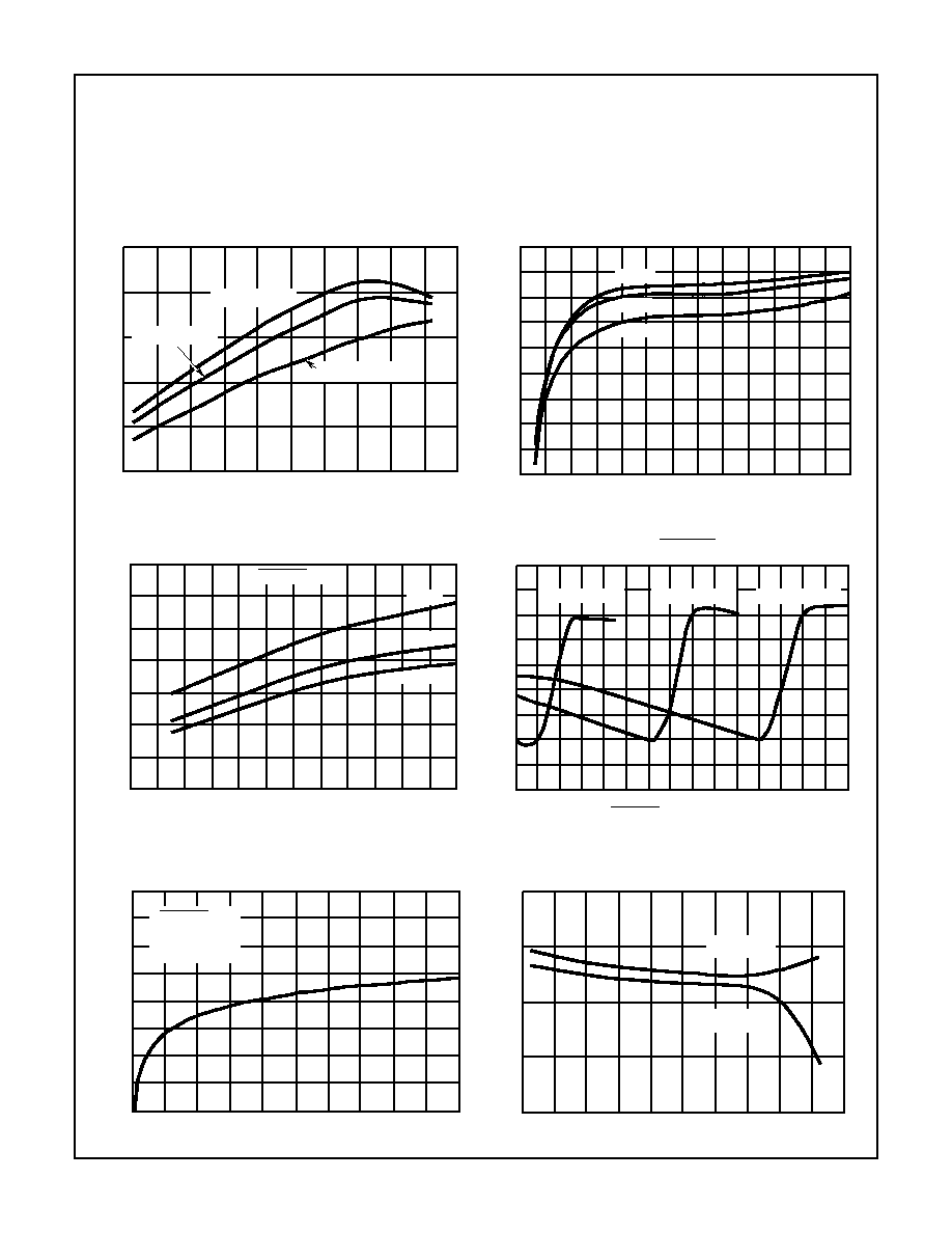
Typical Performance Curves
V
SUPPLY
=
�
15V, A
V
= +1, R
F
= 1k
, R
L
= 400
, T
A
= +25
o
C, Unless Otherwise Specified
INPUT NOISE vs FREQUENCY
Average of 18 Units from 3 Lots
INPUT OFFSET VOLTAGE vs TEMPERATURE
Absolute Value Average of 30 Units from 3 Lots
+INPUT BIAS CURRENT vs TEMPERATURE
Average of 30 Units from 3 Lots
-INPUT BIAS CURRENT vs TEMPERATURE
Absolute Value Average of 30 Units from 3 Lots
FREQUENCY (Hz)
10
100
1K
10K
100K
1
10
100
1
10
100
INPUT NOISE V
O
L
T
A
GE (nV
Hz)
INPUT NOISE CURRENT (pA
Hz)
A
V
= +10
-INPUT NOISE CURRENT
INPUT NOISE VOLTAGE
+INPUT NOISE CURRENT
TEMPERATURE (
o
C)
-60
-40
-20
0
20
40
60
80
100
120
140
OFFSET V
O
L
T
A
GE (mV)
2.5
2.0
1.5
1.0
0.5
0.0
V
SUPPLY
=
�
15V
V
SUPPLY
=
�
4.5V
V
SUPPLY
=
�
10V
TEMPERATURE (
o
C)
-60
-40
-20
0
20
40
60
80
100
120
140
0
-0.5
-1.0
-1.5
-2.0
-2.5
V
SUPPLY
=
�
15V
V
SUPPLY
=
�
4.5V
V
SUPPLY
=
�
10V
BIAS CURRENT (
�
A)
TEMPERATURE (
o
C)
-60
-40
-20
0
20
40
60
80
100
120
140
BIAS CURRENT (
�
A)
2.0
1.8
1.6
1.4
1.2
1.0
V
SUPPLY
=
�
15V
V
SUPPLY
=
�
4.5V
V
SUPPLY
=
�
10V
HA-5020
100MHz Current Feedback
Video Amplifier with Disable
Spec Number
511080-883
DESIGN INFORMATION
(Continued)
The information contained in this section has been developed through characterization by Harris Semiconductor and is for use as application
and design information only. No guarantee is implied.
3-107
HA-5020
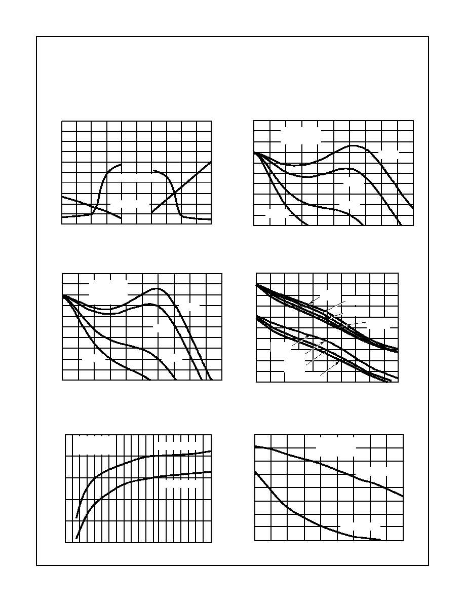
TRANSIMPEDANCE vs TEMPERATURE
Average of 30 Units from 3 Lots
SUPPLY CURRENT vs SUPPLY VOLTAGE
Average of 30 Units from 3 Lots
DISABLE SUPPLY CURRENT vs SUPPLY VOLTAGE
Average of 30 Units from 3 Lots
SUPPLY CURRENT vs DISABLE INPUT VOLTAGE
DISABLE MODE FEEDTHROUGH vs FREQUENCY
DISABLED OUTPUT LEAKAGE vs TEMPERATURE
Average of 30 Units from 3 Lots
Typical Performance Curves
V
SUPPLY
=
�
15V, A
V
= +1, R
F
= 1k
, R
L
= 400
, T
A
= +25
o
C, Unless Otherwise Specified
TEMPERATURE (
o
C)
-60
-40
-20
0
20
40
60
80
100
120
140
OPEN LOOP GAIN (M
)
6
5
4
3
2
1
V
SUPPLY
=
�
15V
V
SUPPLY
=
�
4.5V
V
SUPPLY
=
�
10V
SUPPLY VOLTAGE (
�
V)
3
SUPPL
Y CURRENT (mA)
5
7
9
11
13
15
4
5
6
7
8
+125
o
C
+25
o
C
-55
o
C
SUPPLY VOLTAGE (
�
V)
3
SUPPL
Y CURRENT (mA)
5
7
9
11
13
15
0
4
5
6
7
+125
o
C
+25
o
C
-55
o
C
1
2
3
DISABLE = 0V
DISABLE INPUT VOLTAGE (V)
1
3
5
7
9
11
13
15
SUPPL
Y CURRENT (mA)
5
4
3
2
1
0
6
7
8
9
V
SUPPLY
=
�
15V
V
SUPPLY
=
�
4.5V
V
SUPPLY
=
�
10V
0
-10
-20
-30
-40
-50
-60
-70
-80
FEEDTHR
OUGH (dB)
0
2
4
6
8
12
14
10
16
18
20
FREQUENCY (MHz)
DISABLE = 0V
V
IN
= 5Vp-p
R
F
= 750
TEMPERATURE (
o
C)
-60
-40
-20
0
20
40
60
80
100
120
140
OUTPUT LEAKA
GE CURRENT (
�
A)
1.0
0.5
0
-0.5
-1.0
V
OUT
= +10V
V
OUT
= -10V
Spec Number
511080-883
DESIGN INFORMATION
(Continued)
The information contained in this section has been developed through characterization by Harris Semiconductor and is for use as application
and design information only. No guarantee is implied.
3-108
HA-5020
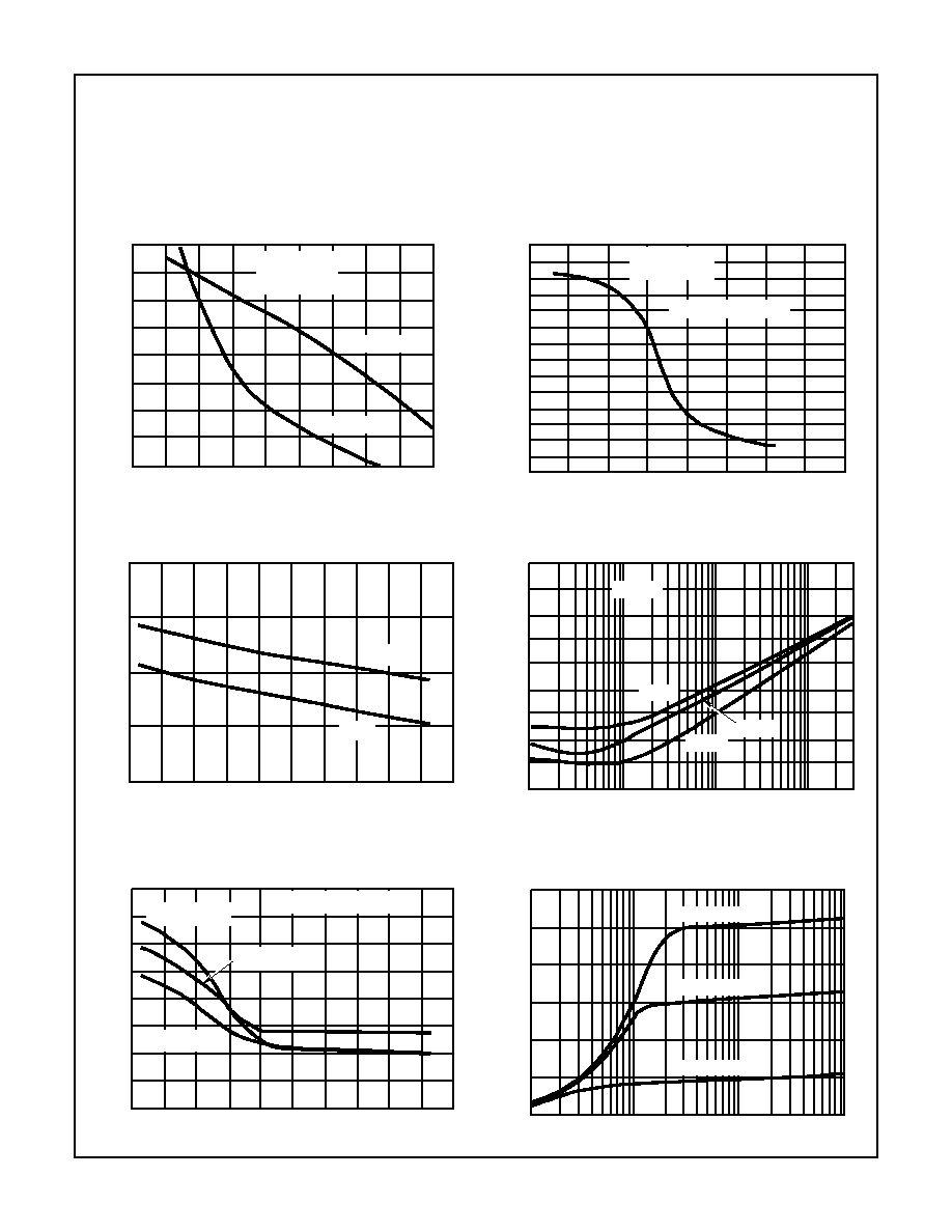
ENABLE/DISABLE TIME vs OUTPUT VOLTAGE
Average of 9 Units from 3 Lots
NON-INVERTING GAIN vs FREQUENCY
INVERTING FREQUENCY RESPONSE
PHASE vs FREQUENCY
BANDWIDTH AND GAIN PEAKING vs LOAD RESISTANCE
BANDWIDTH AND GAIN PEAKING vs FEEDBACK RESISTANCE
Typical Performance Curves
V
SUPPLY
=
�
15V, A
V
= +1, R
F
= 1k
, R
L
= 400
, T
A
= +25
o
C, Unless Otherwise Specified
OUTPUT VOLTAGE (V)
-10
-8
-6
-4
-2
0
2
4
6
8
10
ENABLE TIME (
�
s)
2.0
1.6
1.2
0.8
0.4
0.0
1.8
1.4
1.0
0.6
0.2
DISABLE TIME (
�
s)
20
16
12
8
4
0
18
14
10
6
2
ENABLE TIME
DISABLE TIME
FREQUENCY (MHz)
0
24
48
72
96
120
-7
-6
-5
-4
-3
-2
-1
0
+1
+2
+3
NORMALIZED GAIN (dB)
V
OUT
= 0.2Vpp
C
L
= 10pF
A
V
= +1
A
V
= +2
A
V
= +6
A
V
= +10
FREQUENCY (MHz)
0
24
48
72
96
120
-7
-6
-5
-4
-3
-2
-1
0
+1
+2
NORMALIZED GAIN (dB)
V
OUT
= 0.2Vpp
C
L
= 10pF
A
V
= -1
A
V
= -2
A
V
= -6
A
V
= -10
R
F
= 750
-8
FREQUENCY (MHz)
0
24
48
72
96
120
-225
-180
-135
-90
-45
0
+45
A
V
= -1
A
V
= -2
A
V
= -6
A
V
= -10
-270
-135
-90
-45
+45
+90
+135
+180
-180
0
INVER
TING PHASE (DEGREES)
NON-INVER
TING PHASE (DEGREES)
A
V
= +1
A
V
= +2
A
V
= +6
A
V
= +10
LOAD RESISTANCE (
)
-3dB B
AND
WIDTH (MHz)
GAIN PEAKING (dB)
0
200
400
600
800
1000
60
70
80
90
100
110
0
1
2
3
4
5
GAIN PEAKING
-3dB BANDWIDTH
C
L
= 10pF
V
OUT
= 0.2Vp-p
FEEDBACK RESISTOR (
)
700
900
1.1K
1.3K
1.5K
85
90
95
100
105
0
5
10
15
20
-3dB B
AND
WIDTH (MHz)
GAIN PEAKING (dB)
GAIN PEAKING
-3dB BANDWIDTH
C
L
= 10pF
V
OUT
= 0.2Vp-p
Spec Number
511080-883
DESIGN INFORMATION
(Continued)
The information contained in this section has been developed through characterization by Harris Semiconductor and is for use as application
and design information only. No guarantee is implied.
3-109
HA-5020
BANDWIDTH AND GAIN PEAKING vs FEEDBACK RESISTANCE
(A
V
= +2)
BANDWIDTH vs FEEDBACK RESISTANCE
(A
V
= +10)
REJECTION RATIOS vs TEMPERATURE
Average of 30 Units from 3 Lots
REJECTION RATIOS vs FREQUENCY
OUTPUT SWING OVERHEAD vs TEMPERATURE
Average of 30 Units from 3 Lots
OUTPUT VOLTAGE SWING vs LOAD RESISTANCE
Typical Performance Curves
V
SUPPLY
=
�
15V, A
V
= +1, R
F
= 1k
, R
L
= 400
, T
A
= +25
o
C, Unless Otherwise Specified
FEEDBACK RESISTOR (
)
400
600
800
1.0K
1.2K
80
85
90
95
100
-3dB B
AND
WIDTH (MHz)
GAIN PEAKING
-3dB BANDWIDTH
C
L
= 10pF
V
OUT
= 0.2Vp-p
0
5
10
15
20
GAIN PEAKING (dB)
FEEDBACK RESISTOR (
)
200
400
600
800
1000
40
50
60
70
80
-3dB B
AND
WIDTH (MHz)
GAIN PEAKING = 0dB
C
L
= 10pF
V
OUT
= 0.2Vp-p
30
20
10
TEMPERATURE (
o
C)
-60
-40
-20
0
20
40
60
80
100
120
140
REJECTION RA
TIO (dB)
75
70
65
60
55
PSRR
CMRR
FREQUENCY (Hz)
10K
100K
1M
10M
REJECTION RA
TIO (dB)
-50
-60
-70
-80
-90
+PSRR
CMRR
-40
-30
-20
-10
0
-PSRR
A
V
= +10
TEMPERATURE (
o
C)
OUTPUT SWING O
VERHEAD (
�
V)
1.5
2.0
2.5
3.0
3.5
0
-20
-40
-60
80
100
120
140
60
40
20
V
SUPPLY
=
�
15V
V
SUPPLY
=
�
4.5V
V
SUPPLY
=
�
10V
(
�
V
SUPPLY
) - (
�
V
OUT
)
LOAD RESISTANCE (
)
OUTPUT V
O
L
T
A
GE SWING (Vp-p)
10
15
20
25
30
10K
1K
100
10
5
0
V
SUPPLY
=
�
15V
V
SUPPLY
=
�
4.5V
V
SUPPLY
=
�
10V
Spec Number
511080-883
DESIGN INFORMATION
(Continued)
The information contained in this section has been developed through characterization by Harris Semiconductor and is for use as application
and design information only. No guarantee is implied.
3-110
HA-5020
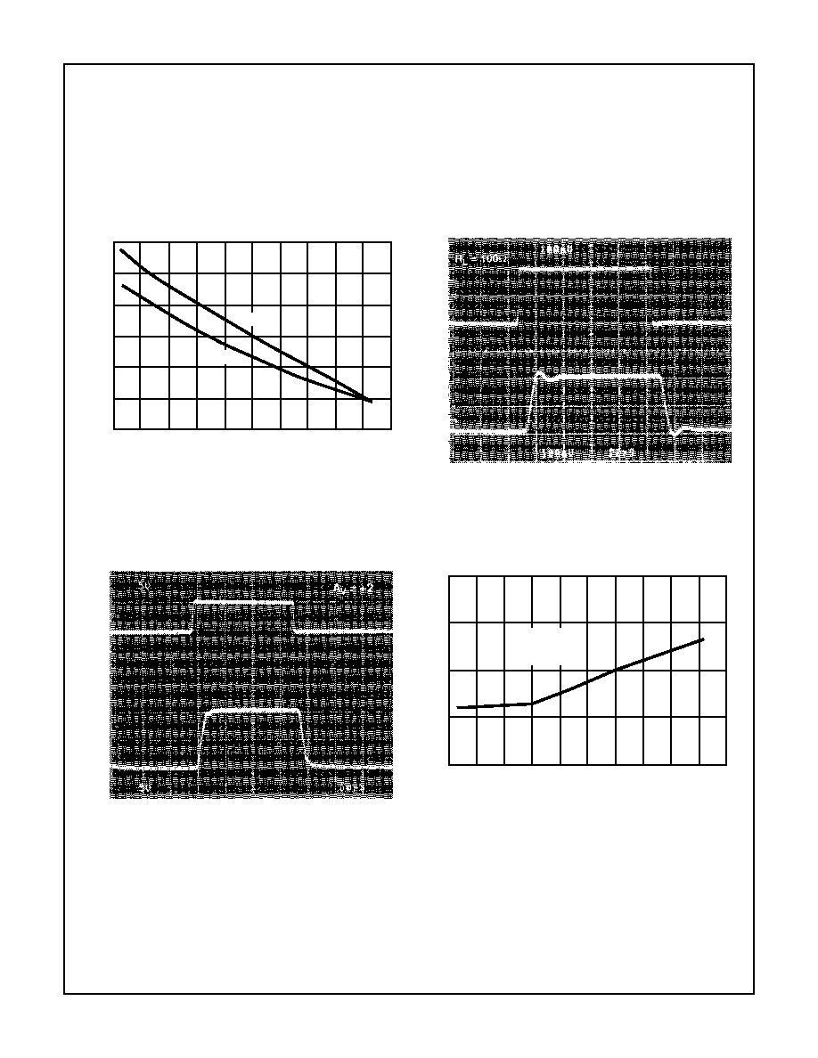
SHORT CIRCUIT CURRENT LIMIT vs TEMPERATURE
SMALL SIGNAL PULSE RESPONSE
Vertical Scale: V
IN
= 100mV/Div.; V
OUT
= 100mV/Div.
Horizontal Scale: 20ns/Div.
LARGE SIGNAL PULSE RESPONSE
Vertical Scale: V
IN
= 5V/Div.; V
OUT
= 5V/Div.
Horizontal Scale: 50ns/Div.
PROPAGATION DELAY vs TEMPERATURE
Average of 18 Units from 3 Lots
Typical Performance Curves
V
SUPPLY
=
�
15V, A
V
= +1, R
F
= 1k
, R
L
= 400
, T
A
= +25
o
C, Unless Otherwise Specified
TEMPERATURE (
o
C)
-60
-40
-20
0
20
40
60
80
100
120
140
40
50
60
70
80
90
100
SHOR
T CIRCUIT CURRENT (mA)
-ISC
+ISC
IN
OUT
IN
OUT
TEMPERATURE (
o
C)
-60
-40
-20
0
20
40
60
80
100
120
140
PR
OP
A
G
A
TION DELA
Y (ns)
7.0
6.5
6.0
5.5
5.0
R
LOAD
= 100
V
OUT
= 1Vp-p
Spec Number
511080-883
DESIGN INFORMATION
(Continued)
The information contained in this section has been developed through characterization by Harris Semiconductor and is for use as application
and design information only. No guarantee is implied.
3-111
HA-5020
PROPAGATION DELAY vs SUPPLY VOLTAGE
Average of 18 Units from 3 Lots
SMALL SIGNAL OVERSHOOT vs LOAD RESISTANCE
DISTORTION vs FREQUENCY
DIFFERENTIAL GAIN vs SUPPLY VOLTAGE
Average of 18 Units from 3 Lots
DIFFERENTIAL PHASE vs SUPPLY VOLTAGE
Average of 18 Units from 3 Lots
SLEW RATE vs TEMPERATURE
Average of 30 Units from 3 Lots
Typical Performance Curves
V
SUPPLY
=
�
15V, A
V
= +1, R
F
= 1k
, R
L
= 400
, T
A
= +25
o
C, Unless Otherwise Specified
SUPPLY VOLTAGE (
�
V)
3
5
7
9
11
13
15
5.0
6.0
7.0
8.0
9.0
10.0
11.0
PR
OP
A
G
A
TION DELA
Y (ns)
A
V
= +10
(R
F
= 383
)
R
LOAD
= 100
V
OUT
= 1Vp-p
A
V
= +2
A
V
= +1
LOAD RESISTANCE (
)
O
VERSHOO
T (%)
10
15
1000
800
600
0
5
0
400
200
V
OUT
= 100mVp-p, C
L
= 10pF
V
SUPPLY
=
�
15V
V
SUPPLY
=
�
5V
A
V
= +2
A
V
= +1
A
V
= +1
A
V
= +2
FREQUENCY (Hz)
1M
10M
DIST
OR
TION (dBc)
-50
-60
-70
-80
-90
HD2
V
O
= 2Vp-p
C
L
= 30pF
HD3
HD3 (GEN)
HD2 (GEN)
3
rd
ORDER IMD
3
rd
ORDER IMD
(GENERATOR)
SUPPLY VOLTAGE (
�
V)
3
5
7
9
11
13
15
DIFFERENTIAL GAIN (%)
0.01
0.02
0.03
0.04
0.05
0.06
0.07
R
LOAD
= 1K
R
LOAD
= 150
R
LOAD
= 75
FREQUENCY = 3.58MHz
SUPPLY VOLTAGE (
�
V)
3
5
7
9
11
13
15
DIFFERENTIAL PHASE (DEGREES)
0.01
0.02
0.03
0.04
0.05
0.06
0.07
R
LOAD
= 1K
R
LOAD
= 150
R
LOAD
= 75
FREQUENCY = 3.58MHz
1200
1000
800
600
-60
SLEW RA
TE (V/
�
s)
-40
-20
0
20
40
60
80
100
120
140
+
SLEW RATE
-
SLEW RATE
V
OUT
= 20Vp-p
TEMPERATURE (
o
C)
Spec Number
511080-883
3-112
All Intersil semiconductor products are manufactured, assembled and tested under ISO9000 quality systems certification.
Intersil products are sold by description only. Intersil Corporation reserves the right to make changes in circuit design and/or specifications at any time without
notice. Accordingly, the reader is cautioned to verify that data sheets are current before placing orders. Information furnished by Intersil is believed to be accurate
and reliable. However, no responsibility is assumed by Intersil or its subsidiaries for its use; nor for any infringements of patents or other rights of third parties which
may result from its use. No license is granted by implication or otherwise under any patent or patent rights of Intersil or its subsidiaries.
For information regarding Intersil Corporation and its products, see web site http://www.intersil.com
Sales Office Headquarters
NORTH AMERICA
Intersil Corporation
P. O. Box 883, Mail Stop 53-204
Melbourne, FL 32902
TEL: (321) 724-7000
FAX: (321) 724-7240
EUROPE
Intersil SA
Mercure Center
100, Rue de la Fusee
1130 Brussels, Belgium
TEL: (32) 2.724.2111
FAX: (32) 2.724.22.05
ASIA
Intersil (Taiwan) Ltd.
Taiwan Limited
7F-6, No. 101 Fu Hsing North Road
Taipei, Taiwan
Republic of China
TEL: (886) 2 2716 9310
FAX: (886) 2 2715 3029
HA-5020
TYPICAL PERFORMANCE CHARACTERISTICS
Device Characterized at: Supply Voltage =
�
15V, R
F
= 1k
, A
V
= +1V/V, R
L
= 400
, C
L
10pF, V
DISABLE
= V+, Unless Otherwise Specified
PARAMETERS
CONDITIONS
TEMPERATURE
TYPICAL
DESIGN
LIMIT
UNITS
Input Offset Voltage
V
CM
= 0V
+25
o
C
2
Table 1
mV
Average Offset Voltage Drift
Versus Temperature
Full
10
15
�
V/
o
C
Positive Input Bias Current
V
CM
= 0V
+25
o
C
3
Table 1
�
A
Negative Input Bias Current
V
CM
= 0V
+25
o
C
12
Table 1
�
A
Input Common Mode Range
Full
�
12
Table 1
V
Offset Voltage Adjustment
See Note 4, Table 1
Full
�
40
Table 1
mV
Output Voltage Swing
V
IN
=
�
12.8
+25
o
C to +125
o
C
�
12.7
Table 1
V
V
IN
=
�
12.8
-55
o
C to 0
o
C
�
11.8
Table 1
V
Output Current
Implied by V
OUT
/400
+25
o
C
31.7
Table 1
mA
Output Short Circuit Current
V
IN
=
�
10V, V
OUT
= 0V
+25
o
C
65
Table 1
mA
Quiescent Supply Current
R
L
= Open
Full
7.5
Table 1
mA
Supply Current, Disabled
R
L
= Open, V
DIS
= 0V
Full
5.0
Table 1
mA
Slew Rate
V
IN
= 20Vp-p
+25
o
C
�
800
Table 2
V/
�
s
Overshoot
V
O
= 1Vp-p, R
L
= 100
+25
o
C
7
Table 3
%
Input Noise Voltage
f = 1kHz
+25
o
C
4.5
8
Positive Input Noise Current
f = 1kHz
+25
o
C
2.5
4
Negative Input Noise Current
f = 1kHz
+25
o
C
25
40
Differential Gain
R
L
= 150
, NTC-7 Composite
+25
o
C
0.025
0.05
%
Differential Phase
R
L
= 150
, NTC-7 Composite
+25
o
C
0.025
0.05
Degrees
nV
Hz
/
pA
Hz
/
pA
Hz
/
Spec Number
511080-883