3-159
CAUTION: These devices are sensitive to electrostatic discharge; follow proper IC Handling Procedures.
http://www.intersil.com or 407-727-9207
|
Copyright
©
Intersil Corporation 1999
HA-5177/883
Ultra Low Offset Voltage Operational Amplifier
Description
The HA-5177/883 is a monolithic, all bipolar, precision oper-
ational amplifier, utilizing Intersil Dielectric Isolation and
advance processing techniques. This design features a
combination of precision input characteristics, wide gain
bandwidth (2MHz) and high speed (0.5V/
µ
s min) and is an
improved version of the HA-5135/883.
The HA-5177/883 uses advanced matching techniques and
laser trimming to produce low offset voltage (10
µ
V typ, 60
µ
V
max) and low offset voltage drift (0.1
µ
V/
o
C typ, 0.6
µ
V/
o
C
max). This design also features low voltage noise (9nV/
Hz
typ), Low current noise (0.32pA/
Hz typ), nanoamp input
currents, and 126dB minimum gain.
These outstanding features along with high CMRR (140dB
typ, 110dB min) and high PSRR (135dB typ, 110dB min)
make this unity gain stable amplifier ideal for high resolution
data acquisition systems, precision integrators, and low level
transducer amplifiers.
Ordering Information
PART
NUMBER
TEMPERATURE
RANGE
PACKAGE
HA2-5177/883
-55
o
C to +125
o
C
8 Pin Can
HA7-5177/883
-55
o
C to +125
o
C
8 Lead CerDIP
HA4-5177/883
-55
o
C to +125
o
C
20 Lead Ceramic LCC
Features
∑ This Circuit is Processed in Accordance to MIL-STD-
883 and is Fully Conformant Under the Provisions of
Paragraph 1.2.1.
∑ Low Offset Voltage. . . . . . . . . . . . . . . . . . . . .60
µ
V (Max)
10
µ
V (Typ)
∑ Low Offset Voltage Drift . . . . . . . . . . . . 0.6
µ
V/
o
C (Max)
0.1
µ
V/
o
C (Typ)
∑ High Voltage Gain . . . . . . . . . . . . . . . . . . . . 126dB (Min)
150dB (Typ)
∑ High CMRR . . . . . . . . . . . . . . . . . . . . . . . . . . 110dB (Min)
140dB (Typ)
∑ High PSRR . . . . . . . . . . . . . . . . . . . . . . . . . . 110dB (Min)
135dB (Typ)
∑ Low Noise . . . . . . . . . . . . . . . . . . . . . . . . 11nV/
Hz (Max)
9nV/
Hz (Typ)
∑ Low Power Consumption . . . . . . . . . . . . . 51mW (Max)
∑ Wide Gain Bandwidth Product . . . . . . . . . . 2MHz (Min)
∑ Unity Gain Stable
Applications
∑ High Gain Instrumentation Amplifiers
∑ Precision Control Systems
∑ Precision Integrators
∑ High Resolution Data Converters
∑ Precision Threshold Detectors
∑ Low Level Transducer Amplifiers
July 1994
Spec Number
511041-883
File Number
3733.1
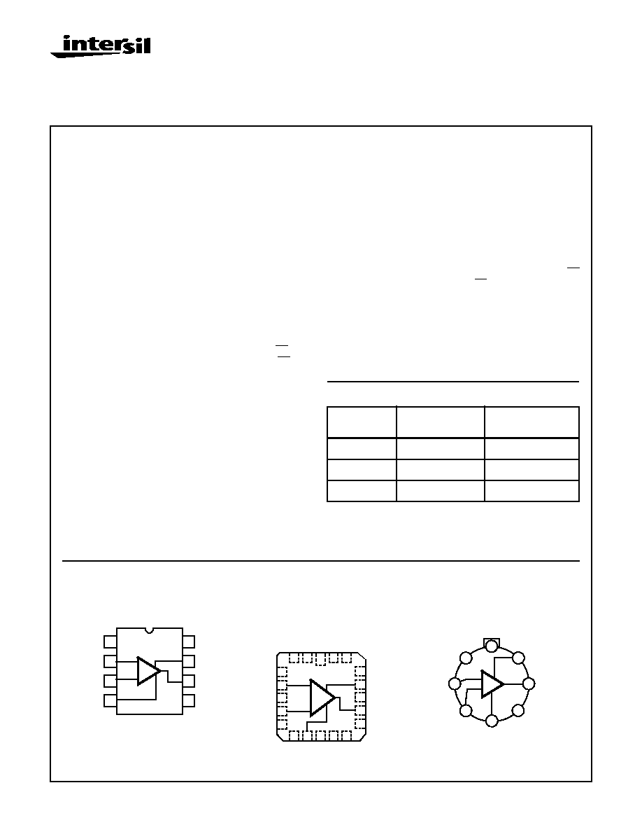
Pinouts
HA-5177/883
(CERDIP)
TOP VIEW
HA-5177/883
(CLCC)
TOP VIEW
HA-5177/883
(METAL CAN)
TOP VIEW
1
2
3
4
8
7
6
5
BAL1
V+
OUT
NC
BAL 2
IN-
IN+
V-
+
-
4
5
6
7
8
9
10 11 12 13
3
2
1 20 19
15
14
18
17
16
BAL 2
NC
V-
NC
NC
NC
NC
NC
V+
OUT
NC
NC
NC
NC
BAL1
NC
NC
+
-IN
+IN
NC
-
BAL1
OUT
IN -
V -
BAL 2
IN+
V+
NC
2
4
6
1
3
7
5
8
+
-
3-160
Specifications HA-5177/883
Absolute Maximum Ratings
Thermal Information
Voltage Between V+ and V- Terminals . . . . . . . . . . . . . . . . . . . . 44V
Differential Input Voltage (Note 1) . . . . . . . . . . . . . . . . . . . . . . . . 7V
Voltage at Either Input Terminal . . . . . . . . . . . . . . . . . . . . . . V+ to V-
Input Current. . . . . . . . . . . . . . . . . . . . . . . . . . . . . . . . . . . . . . . 25mA
Output Current . . . . . . . . . . . . . . . . . . . .Full Short Circuit Protection
Junction Temperature (T
J
) . . . . . . . . . . . . . . . . . . . . . . . . . . +175
o
C
Storage Temperature Range . . . . . . . . . . . . . . . . . -65
o
C to +150
o
C
ESD Rating. . . . . . . . . . . . . . . . . . . . . . . . . . . . . . . . . . . . . . <2000V
Lead Temperature (Soldering 10s) . . . . . . . . . . . . . . . . . . . . +300
o
C
Thermal Resistance
JA
JC
CerDIP Package . . . . . . . . . . . . . . . . . . .
115
o
C/W
28
o
C/W
Ceramic LCC Package . . . . . . . . . . . . . .
65
o
C/W
15
o
C/W
Metal Can Package . . . . . . . . . . . . . . . . .
155
o
C/W
67
o
C/W
Package Power Dissipation Limit at +75
o
C for T
J
+175
o
C
CerDIP Package . . . . . . . . . . . . . . . . . . . . . . . . . . . . . . . . 870mW
Ceramic LCC Package . . . . . . . . . . . . . . . . . . . . . . . . . . . . 1.54W
Metal Can Package . . . . . . . . . . . . . . . . . . . . . . . . . . . . . . 645mW
Package Power Dissipation Derating Factor Above +75
o
C
CerDIP Package . . . . . . . . . . . . . . . . . . . . . . . . . . . . . . 8.7mW/
o
C
Ceramic LCC Package . . . . . . . . . . . . . . . . . . . . . . . . 15.4mW/
o
C
Metal Can Package . . . . . . . . . . . . . . . . . . . . . . . . . . . . 6.5mW/
o
C
CAUTION: Stresses above those listed in "Absolute Maximum Ratings" may cause permanent damage to the device. This is a stress only rating and operation
of the device at these or any other conditions above those indicated in the operational sections of this specification is not implied.
Operating Conditions
Operating Temperature Range . . . . . . . . . . . . . . . . -55
o
C to +125
o
C
Operating Supply Voltage
. . . . . . . . . . . . . . . . . . . . . . . . . . . . . . . . ±
15V
V
INCM
1/2 (V+ - V-)
R
L
600
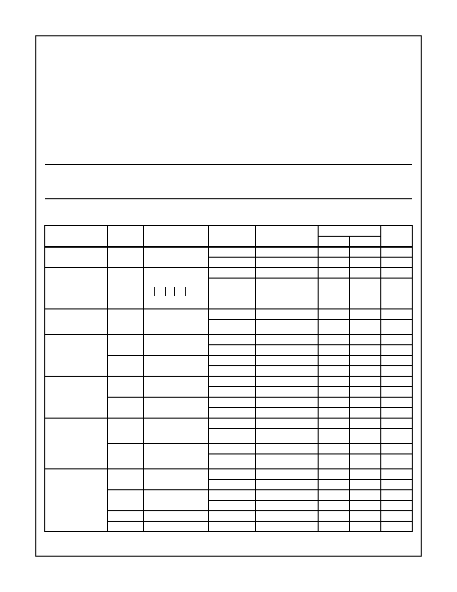
TABLE 1. DC ELECTRICAL PERFORMANCE CHARACTERISTICS
Device Tested at: V
SUPPLY
=
±
15V, R
SOURCE
= 5
0
, R
LOAD
= 100k
, V
OUT
= 0V, Unless Otherwise Specified.
PARAMETERS
SYMBOL
CONDITIONS
GROUP A
SUBGROUPS
TEMPERATURE
LIMITS
UNITS
MIN
MAX
Input Offset Voltage
V
IO
V
CM
= 0V
1
+25
o
C
-60
60
µ
V
2, 3
+125
o
C, -55
o
C
-100
100
µ
V
Input Bias Current
I
B
V
CM
= 0V,
R
S
= 10k
, 5
0
1
+25
o
C
-6
6
nA
2, 3
+125
o
C, -55
o
C
-8
8
nA
Input Offset Current
I
IO
V
CM
= 0V,
+R
S
= 10k
,
-R
S
= 10k
1
+25
o
C
-6
6
nA
2, 3
+125
o
C, -55
o
C
-8
8
nA
Common Mode
Range
+CMR
V+ = +3V, V- = -27V
1
+25
o
C
12
-
V
2, 3
+125
o
C, -55
o
C
12
-
V
-CMR
V+ = +27V, V- = -3V
1
+25
o
C
-
-12
V
2, 3
+125
o
C, -55
o
C
-
-12
V
Large Signal Voltage
Gain
+A
VOL
V
OUT
= 0V and +10V,
R
L
= 2k
4
+25
o
C
126
-
dB
5, 6
+125
o
C, -55
o
C
120
-
dB
-A
VOL
V
OUT
= 0V and -10V,
R
L
= 2k
4
+25
o
C
126
-
dB
5, 6
+125
o
C, -55
o
C
120
-
dB
Common Mode
Rejection Ratio
+CMRR
V
CM
= 10V,
V+ = +5V, V- = - 25V,
V
OUT
= -10
1
+25
o
C
116
-
dB
2, 3
+125
o
C, -55
o
C
110
-
dB
-CMRR
V
CM
= 10V,
V+ = +25V, V- = - 5V,
V
OUT
= +10
1
+25
o
C
116
-
dB
2, 3
+125
o
C, -55
o
C
110
-
dB
Output Voltage
Swing
+V
OUT1
R
L
= 2k
4
+25
o
C
12
-
V
5, 6
+125
o
C, -55
o
C
12
-
V
-V
OUT1
R
L
= 2k
4
+25
o
C
-
-12
V
5, 6
+125
o
C, -55
o
C
-
-12
V
+V
OUT2
R
L
= 600
4
+25
o
C
10
-
V
-V
OUT2
R
L
= 600
4
+25
o
C
-
-10
V
+I
B
I
≠
B
+
2
-----------------------------
Spec Number
511041-883
3-161
Spec Number
511041-883
Specifications HA-5177/883
Output Current
+I
OUT
V
OUT
= -10V
4
+25
o
C
15
-
mA
5, 6
+125
o
C, -55
o
C
15
-
mA
-I
OUT
V
OUT
= +10V
4
+25
o
C
-
-15
mA
5, 6
+125
o
C, -55
o
C
-
-15
mA
Quiescent Power
Supply Current
+I
CC
V
OUT
= 0V, I
OUT
= 0mA
1
+25
o
C
-
1.7
mA
2, 3
+125
o
C, -55
o
C
-
1.7
mA
-I
CC
V
OUT
= 0V, I
OUT
= 0mA
1
+25
o
C
-1.7
-
mA
2, 3
+125
o
C, -55
o
C
-1.7
-
mA
Power Supply
Rejection Ratio
+PSRR
V
SUP
= 15V,
V+ = +5V, V- = - 15V,
V+ = +20V, V- = - 15V
1
+25
o
C
110
-
dB
2, 3
+125
o
C, -55
o
C
110
-
dB
-PSRR
V
SUP
= 15V,
V+ = +15V, V- = - 5V,
V+ = +15V, V- = - 20V
1
+25
o
C
110
-
dB
2, 3
+125
o
C, -55
o
C
110
-
dB
Offset Voltage
Adjustment
+V
IO
Adj
Note 2
1
+25
o
C
0.3
-
mV
2, 3
+125
o
C, -55
o
C
0.3
-
mV
-V
IO
Adj
Note 2
1
+25
o
C
-
-0.3
mV
2, 3
+125
o
C, -55
o
C
-
-0.3
mV
NOTES:
1. The input stage has series 500
resistors along with back to back diodes. This provides large differential input voltage protection for a
slight increase in noise voltage.
2. This test is for functionality only to assure adjustment through 0V.
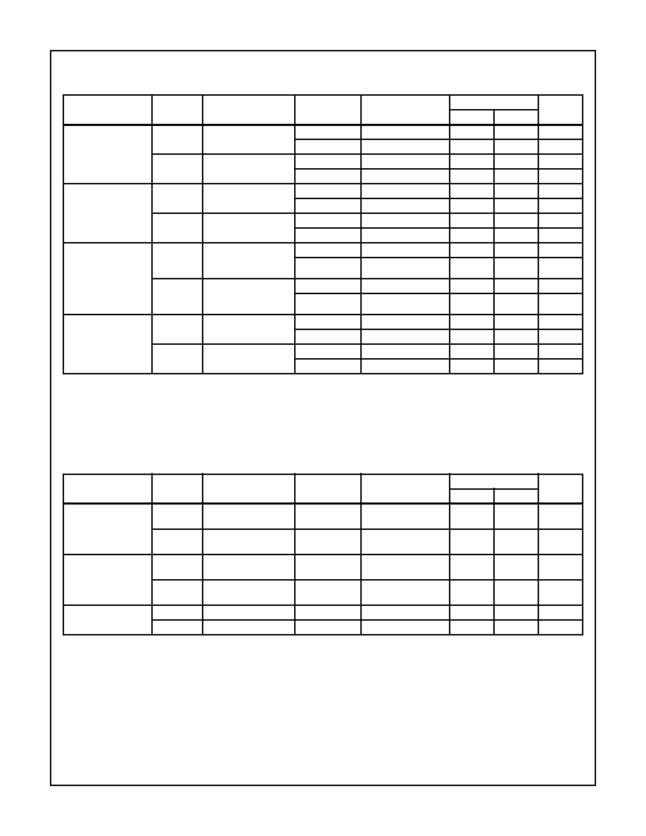
TABLE 2. AC ELECTRICAL PERFORMANCE CHARACTERISTICS
Device Tested at: V
SUPPLY
=
±
15V, R
SOURCE
= 50
, R
LOAD
= 2k
, C
LOAD
= 50pF, A
VCL
= +1V/V, Unless Otherwise Specified.
PARAMETERS
SYMBOL
CONDITIONS
GROUP A
SUBGROUPS
TEMPERATURE
LIMITS
UNITS
MIN
MAX
Slew Rate
+SR
V
OUT
= -3V to +3V,
V
IN
S.R.
25V/
µ
s
7
+25
o
C
0.5
-
V/
µ
s
-SR
V
OUT
= +3V to -3V,
V
IN
S.R.
25V/
µ
s
7
+25
o
C
0.5
-
V/
µ
s
Rise and Fall Time
t
R
V
OUT
= 0 to +200mV
10%
T
R
90%
7
+25
o
C
-
420
ns
t
F
V
OUT
= 0 to -200mV
10%
T
F
90%
7
+25
o
C
-
420
ns
Overshoot
+OS
V
OUT
= 0 to +200mV
7
+25
o
C
-
40
%
-OS
V
OUT
= 0 to -200mV
7
+25
o
C
-
40
%
TABLE 1. DC ELECTRICAL PERFORMANCE CHARACTERISTICS (Continued)
Device Tested at: V
SUPPLY
=
±
15V, R
SOURCE
= 5
0
, R
LOAD
= 100k
, V
OUT
= 0V, Unless Otherwise Specified.
PARAMETERS
SYMBOL
CONDITIONS
GROUP A
SUBGROUPS
TEMPERATURE
LIMITS
UNITS
MIN
MAX
3-162
Spec Number
511041-883
Specifications HA-5177/883
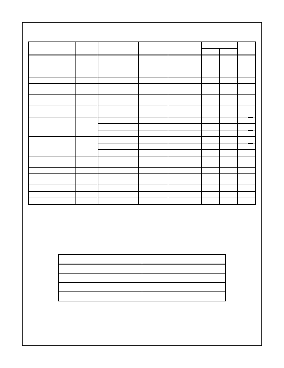
TABLE 3. ELECTRICAL PERFORMANCE CHARACTERISTICS
Device Characterized at: V
SUPPLY
=
±
15V, R
LOAD
= 2k
, C
LOAD
= 50pF, A
V
= +1V/V, Unless Otherwise Specified.
PARAMETERS
SYMBOL
CONDITIONS
NOTES
TEMPERATURE
LIMITS
UNITS
MIN
MAX
Average Offset Voltage
Drift
V
IO
TC
V
CM
= 0V
1
-55
o
C to +125
o
C
-
0.6
µ
V/
o
C
Average Offset Current
Drift
I
IO
TC
Versus Temperature
1
-55
o
C to +125
o
C
-
40
pA/
o
C
Average Bias Current Drift
I
R
TC
Versus Temperature
1
-55
o
C to +125
o
C
-
40
pA/
o
C
Differential Input
Resistance
R
IN
V
CM
= 0V
1
+25
o
C
20
-
M
Low Frequency
Peak-to-Peak Noise Voltage
E
NP-P
0.1Hz to 10Hz
1
+25
o
C
-
0.6
µ
V
P-P
Low Frequency
Peak-to-Peak Noise Current
I
NP-P
0.1Hz to 10Hz
1
+25
o
C
-
45
pA
P-P
Input Noise Voltage
Density
E
N
R
S
= 20
, f
O
= 10Hz
1
+25
o
C
-
18
nV
/
Hz
R
S
= 20
, f
O
= 100Hz
1
+25
o
C
-
13
nV
/
Hz
R
S
= 20
, f
O
= 1kHz
1
+25
o
C
-
11
nV
/
Hz
Input Noise Current
Density
I
N
R
S
= 2M
, f
O
= 10Hz
1
+25
o
C
-
4
pA
/
Hz
R
S
= 2M
, f
O
= 100Hz
1
+25
o
C
-
2.3
pA
/
Hz
R
S
= 2M
, f
O
= 1kHz
1
+25
o
C
-
1
pA
/
Hz
Gain Bandwidth Product
GBWP
V
O
= 100mV,
1Hz
f
O
100kHz
1
+25
o
C
2
-
MHz
Full Power Bandwidth
FPBW
V
PEAK
= 10V
1, 2
+25
o
C
8
-
kHz
Minimum Closed Loop
Stable Gain
CLSG
R
L
= 2k
, C
L
= 50pF
1
-55
o
C to +125
o
C
+
1
-
V/V
Settling Time
t
S
To 0.1% for a 10V Step
1
+25
o
C
-
15
µ
s
Output Resistance
R
OUT
Open Loop
1
+25
o
C
-
70
Power Consumption
PC
V
OUT
= 0V, I
OUT
= 0mA
1, 3
-55
o
C to +125
o
C
-
51
mW
NOTES:
1. Parameters listed in Table 3 are controlled via design or process parameters and are not directly tested at final production. These param-
eters are lab characterized upon initial design release, or upon design changes. These parameters are guaranteed by characterization
based upon data from multiple production runs which reflect lot to lot and within lot variation.
2. Full Power Bandwidth guarantee based on Slew Rate measurement using FPBW = Slew Rate/(2
V
PEAK
).
3. Power Consumption based upon Quiescent Supply Current test maximum. (No load on outputs.)
TABLE 4. ELECTRICAL TEST REQUIREMENTS
MIL-STD-883 TEST REQUIREMENTS
SUBGROUPS (SEE TABLES 1 AND 2)
Interim Electrical Parameters (Pre Burn-In)
1
Final Electrical Test Parameters
1 (Note 1), 2, 3, 4, 5, 6, 7
Group A Test Requirements
1, 2, 3, 4, 5, 6, 7
Groups C and D Endpoints
1
NOTE:
1. PDA applies to Subgroup 1 only.
3-163
All Intersil semiconductor products are manufactured, assembled and tested under ISO9000 quality systems certification.
Intersil products are sold by description only. Intersil Corporation reserves the right to make changes in circuit design and/or specifications at any time without
notice. Accordingly, the reader is cautioned to verify that data sheets are current before placing orders. Information furnished by Intersil is believed to be accurate
and reliable. However, no responsibility is assumed by Intersil or its subsidiaries for its use; nor for any infringements of patents or other rights of third parties which
may result from its use. No license is granted by implication or otherwise under any patent or patent rights of Intersil or its subsidiaries.
For information regarding Intersil Corporation and its products, see web site http://www.intersil.com
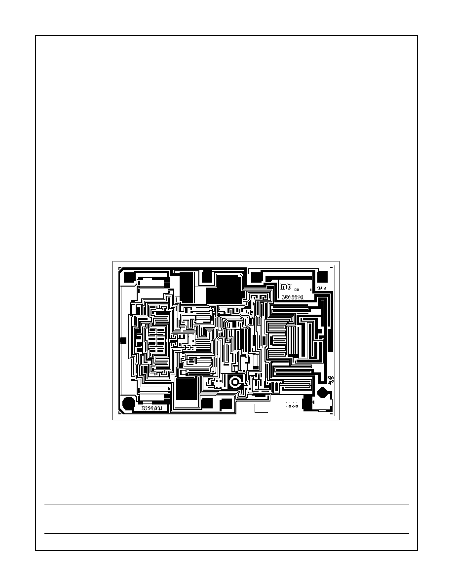
HA-5177/883
Die Characteristics
DIE DIMENSIONS:
72 x 103 x 19 mils
±
1 mils
1840 x 2620 x 483
µ
m
±
25.4
µ
m
METALLIZATION:
Type: Al, 1% Cu
Thickness: 16k
≈
±
2k
≈
GLASSIVATION:
Type: Nitride (Si3N4) over Silox (SIO2, 5% Phos.)
Silox Thickness: 12k
≈
±
2k
≈
Nitride Thickness: 3.5k
≈
±
1.5k
≈
WORST CASE CURRENT DENSITY:
6.0 x 10
4
A/cm
2
SUBSTRATE POTENTIAL (Powered Up): V-
TRANSISTOR COUNT: 71
PROCESS: Bipolar Dielectric Isolation
Metallization Mask Layout
HA-5177/883
BAL1
V+
OUT
NC
V-
+IN
-IN
BAL2
Spec Number
511041-883