 | –≠–ª–µ–∫—Ç—Ä–æ–Ω–Ω—ã–π –∫–æ–º–ø–æ–Ω–µ–Ω—Ç: HA5022IB | –°–∫–∞—á–∞—Ç—å:  PDF PDF  ZIP ZIP |
1
CAUTION: These devices are sensitive to electrostatic discharge; follow proper IC Handling Procedures.
http://www.intersil.com or 407-727-9207 | Copyright © Intersil Corporation 1999
HA5022
Dual, 125MHz, Video Current Feedback
Amplifier with Disable
The HA5022 is a dual version of the popular Intersil HA5020.
It features wide bandwidth and high slew rate, and is
optimized for video applications and gains between 1 and
10. It is a current feedback amplifier and thus yields less
bandwidth degradation at high closed loop gains than
voltage feedback amplifiers.
The low differential gain and phase, 0.1dB gain flatness, and
ability to drive two back terminated 75
cables, make this
amplifier ideal for demanding video applications.
The HA5022 also features a disable function that
significantly reduces supply current while forcing the output
to a true high impedance state. This functionality allows 2:1
video multiplexers to be implemented with a single IC.
The current feedback design allows the user to take
advantage of the amplifier's bandwidth dependency on the
feedback resistor. By reducing R
F
, the bandwidth can be
increased to compensate for decreases at higher closed
loop gains or heavy output loads.
Features
∑ Dual Version of HA-5020
∑ Individual Output Enable/Disable
∑ Input Offset Voltage . . . . . . . . . . . . . . . . . . . . . . . . 800
µ
V
∑ Wide Unity Gain Bandwidth . . . . . . . . . . . . . . . . . 125MHz
∑ Slew Rate . . . . . . . . . . . . . . . . . . . . . . . . . . . . . . . 475V/
µ
s
∑ Differential Gain . . . . . . . . . . . . . . . . . . . . . . . . . . . 0.03%
∑ Differential Phase . . . . . . . . . . . . . . . . . . . . 0.03 Degrees
∑ Supply Current (per Amplifier) . . . . . . . . . . . . . . . . 7.5mA
∑ ESD Protection. . . . . . . . . . . . . . . . . . . . . . . . . . . . 4000V
∑ Guaranteed Specifications at
±
5V Supplies
Applications
∑ Video Multiplexers; Video Switching and Routing
∑ Video Gain Block
∑ Video Distribution Amplifier/RGB Amplifier
∑ Flash A/D Driver
∑ Current to Voltage Converter
∑ Medical Imaging
∑ Radar and Imaging Systems
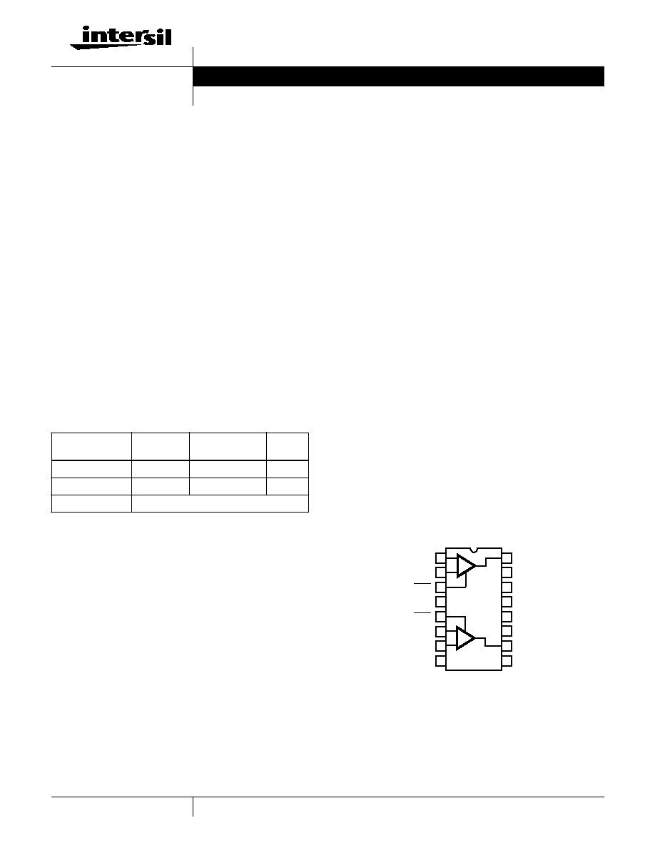
Pinout
HA5022
(PDIP, SOIC)
TOP VIEW
Ordering Information
PART NUMBER
TEMP.
RANGE (
o
C)
PACKAGE
PKG.
NO.
HA5022IP
-40 to 85
16 Ld PDIP
E16.3
HA5022IB
-40 to 85
16 Ld SOIC
M16.15
HA5022EVAL
High Speed Op Amp DIP Evaluation Board
14
15
16
9
13
12
11
10
1
2
3
4
5
7
6
8
-IN1
+IN1
DIS1
V-
DIS2
+IN2
NC
-IN2
OUT1
NC
V+
NC
NC
OUT2
NC
NC
+
-
+
-
Data Sheet
May 1999
File Number
3392.6

2
Absolute Maximum Ratings
Thermal Information
Voltage Between V+ and V- Terminals. . . . . . . . . . . . . . . . . . . . 36V
DC Input Voltage (Note 3) . . . . . . . . . . . . . . . . . . . . . . . .
±
V
SUPPLY
Differential Input Voltage . . . . . . . . . . . . . . . . . . . . . . . . . . . . . . .10V
Output Current (Note 4) . . . . . . . . . . . . . . . . .Short Circuit Protected
ESD Rating (Note 3)
Human Body Model (Per MIL-STD-883 Method 3015.7) . . 2000V
Operating Conditions
Temperature Range . . . . . . . . . . . . . . . . . . . . . . . . . . -40
o
C to 85
o
C
Supply Voltage Range (Typical) . . . . . . . . . . . . . . . . .
±
4.5V to
±
15V
Thermal Resistance (Typical, Note 2)
JA
(
o
C/W)
PDIP Package . . . . . . . . . . . . . . . . . . . . . . . . . . . . .
90
SOIC Package . . . . . . . . . . . . . . . . . . . . . . . . . . . . .
115
Maximum Junction Temperature (Note 1) . . . . . . . . . . . . . . . . .175
o
C
Maximum Junction Temperature (Plastic Package, Note 1) . .150
o
C
Maximum Storage Temperature Range . . . . . . . . . . -65
o
C to 150
o
C
Maximum Lead Temperature (Soldering 10s) . . . . . . . . . . . . 300
o
C
(SOIC - Lead Tips Only)
CAUTION: Stresses above those listed in "Absolute Maximum Ratings" may cause permanent damage to the device. This is a stress only rating and operation of the
device at these or any other conditions above those indicated in the operational sections of this specification is not implied.
NOTES:
1. Maximum power dissipation, including output load, must be designed to maintain junction temperature below 175
o
C for die, and below 150
o
C
for plastic packages. See Application Information section for safe operating area information.
2.
JA
is measured with the component mounted on an evaluation PC board in free air.
3. The non-inverting input of unused amplifiers must be connected to GND.
4. Output is protected for short circuits to ground. Brief short circuits to ground will not degrade reliability, however, continuous (100% duty cycle)
output current should not exceed 15mA for maximum reliability.
Electrical Specifications
V
SUPPLY
=
±
5V, R
F
= 1k
, A
V
= +1, R
L
= 400
,
C
L
10pF, Unless Otherwise Specified
PARAMETER
TEST
CONDITIONS
(NOTE 11)
TEST
LEVEL
TEMP.
(
o
C)
MIN
TYP
MAX
UNITS
INPUT CHARACTERISTICS
Input Offset Voltage (V
IO
)
A
25
-
0.8
3
mV
A
Full
-
-
5
mV
Delta V
IO
Between Channels
A
Full
-
1.2
3.5
mV
Average Input Offset Voltage Drift
B
Full
-
5
-
µ
V/
o
C
V
IO
Common Mode Rejection Ratio
Note 5
A
25
53
-
-
dB
A
Full
50
-
-
dB
V
IO
Power Supply Rejection Ratio
±
3.5V
V
S
±
6.5V
A
25
60
-
-
dB
A
Full
55
-
-
dB
Input Common Mode Range
Note 5
A
Full
±
2.5
-
-
V
Non-Inverting Input (+IN) Current
A
25
-
3
8
µ
A
A
Full
-
-
20
µ
A
+IN Common Mode Rejection
(+I
BCMR
=
)
Note 5
A
25
-
-
0.15
µ
A/V
A
Full
-
-
0.5
µ
A/V
+IN Power Supply Rejection
±
3.5V
V
S
±
6.5V
A
25
-
-
0.1
µ
A/V
A
Full
-
-
0.3
µ
A/V
Inverting Input (-IN) Current
A
25, 85
-
4
12
µ
A
A
-40
-
10
30
µ
A
Delta -IN BIAS Current Between
Channels
A
25, 85
-
6
15
µ
A
A
-40
-
10
30
µ
A
-IN Common Mode Rejection
Note 5
A
25
-
-
0.4
µ
A/V
A
Full
-
-
1.0
µ
A/V
1
+R
IN
HA5022

3
-IN Power Supply Rejection
±
3.5V
V
S
±
6.5V
A
25
-
-
0.2
µ
A/V
A
Full
-
-
0.5
µ
A/V
Input Noise Voltage
f = 1kHz
B
25
-
4.5
-
nV/
Hz
+Input Noise Current
f = 1kHz
B
25
-
2.5
-
pA/
Hz
-Input Noise Current
f = 1kHz
B
25
-
25.0
-
pA/
Hz
TRANSFER CHARACTERISTICS
Transimpedance
Note 16
A
25
1.0
-
-
M
A
Full
0.85
-
-
M
Open Loop DC Voltage Gain
R
L
= 400
, V
OUT
=
±
2.5V
A
25
70
-
-
dB
A
Full
65
-
-
dB
Open Loop DC Voltage Gain
R
L
= 100
, V
OUT
=
±
2.5V
A
25
50
-
-
dB
A
Full
45
-
-
dB
OUTPUT CHARACTERISTICS
Output Voltage Swing
R
L
= 150
A
25
±
2.5
±
3.0
-
V
A
Full
±
2.5
±
3.0
-
V
Output Current
R
L
= 150
B
Full
±
16.6
±
20.0
-
mA
Output Current, Short Circuit
V
IN
=
±
2.5V, V
OUT
= 0V
A
Full
±
40
±
60
-
mA
Output Current, Disabled
V
OUT
=
±
2.5V, V
IN
= 0V,
DISABLE = 0V
A
Full
-
-
2
µ
A
Output Disable Time
Note 12
B
25
-
40
-
µ
s
Output Enable Time
Note 13
B
25
-
40
-
ns
Output Capacitance, Disabled
Note 14
B
25
-
15
-
pF
POWER SUPPLY CHARACTERISTICS
Supply Voltage Range
A
25
5
-
15
V
Quiescent Supply Current
A
Full
-
7.5
10
mA/Op Amp
Supply Current, Disabled
DISABLE = 0V
A
Full
-
5
7.5
mA/Op Amp
Disable Pin Input Current
DISABLE = 0V
A
Full
-
1.0
1.5
mA
Minimum Pin 8 Current to Disable
Note 6
A
Full
350
-
-
µ
A
Maximum Pin 8 Current to Enable
Note 7
A
Full
-
-
20
µ
A
AC CHARACTERISTICS (A
V
= +1)
Slew Rate
Note 8
B
25
275
400
-
V/
µ
s
Full Power Bandwidth
Note 9
B
25
22
28
-
MHz
Rise Time
Note 10
B
25
-
6
-
ns
Fall Time
Note 10
B
25
-
6
-
ns
Propagation Delay
Note 10
B
25
-
6
-
ns
Overshoot
B
25
-
4.5
-
%
-3dB Bandwidth
V
OUT
= 100mV
B
25
-
125
-
MHz
Settling Time to 1%
2V Output Step
B
25
-
50
-
ns
Settling Time to 0.25%
2V Output Step
B
25
-
75
-
ns
Electrical Specifications
V
SUPPLY
=
±
5V, R
F
= 1k
, A
V
= +1, R
L
= 400
,
C
L
10pF, Unless Otherwise Specified (Continued)
PARAMETER
TEST
CONDITIONS
(NOTE 11)
TEST
LEVEL
TEMP.
(
o
C)
MIN
TYP
MAX
UNITS
HA5022

4
AC CHARACTERISTICS (A
V
= +2, R
F
= 681
)
Slew Rate
Note 8
B
25
-
475
-
V/
µ
s
Full Power Bandwidth
Note 9
B
25
-
26
-
MHz
Rise Time
Note 10
B
25
-
6
-
ns
Fall Time
Note 10
B
25
-
6
-
ns
Propagation Delay
Note 10
B
25
-
6
-
ns
Overshoot
B
25
-
12
-
%
-3dB Bandwidth
V
OUT
= 100mV
B
25
-
95
-
MHz
Settling Time to 1%
2V Output Step
B
25
-
50
-
ns
Settling Time to 0.25%
2V Output Step
B
25
-
100
-
ns
Gain Flatness
5MHz
B
25
-
0.02
-
dB
20MHz
B
25
-
0.07
-
dB
AC CHARACTERISTICS (A
V
= +10, R
F
= 383
)
Slew Rate
Note 8
B
25
350
475
-
V/
µ
s
Full Power Bandwidth
Note 9
B
25
28
38
-
MHz
Rise Time
Note 10
B
25
-
8
-
ns
Fall Time
Note 10
B
25
-
9
-
ns
Propagation Delay
Note 10
B
25
-
9
-
ns
Overshoot
B
25
-
1.8
-
%
-3dB Bandwidth
V
OUT
= 100mV
B
25
-
65
-
MHz
Settling Time to 1%
2V Output Step
B
25
-
75
-
ns
Settling Time to 0.1%
2V Output Step
B
25
-
130
-
ns
VIDEO CHARACTERISTICS
Differential Gain (Note 15)
R
L
= 150
B
25
-
0.03
-
%
Differential Phase (Note 15)
R
L
= 150
B
25
-
0.03
-
Degrees
NOTES:
5. V
CM
=
±
2.5V. At -40
o
C Product is tested at V
CM
=
±
2.25V because short test duration does not allow self heating.
6. R
L
= 100
, V
IN
= 2.5V. This is the minimum current which must be pulled out of the Disable pin in order to disable the output. The output is
considered disabled when -10mV
V
OUT
+10mV.
7. V
IN
= 0V. This is the maximum current that can be pulled out of the Disable pin with the HA5022 remaining enabled. The HA5022 is
considered disabled when the supply current has decreased by at least 0.5mA.
8. V
OUT
switches from -2V to +2V, or from +2V to -2V. Specification is from the 25% to 75% points.
9.
.
10. R
L
= 100
, V
OUT
= 1V. Measured from 10% to 90% points for rise/fall times; from 50% points of input and output for propagation delay.
11. A. Production Tested; B. Typical or Guaranteed Limit based on characterization; C. Design Typical for information only.
12. V
IN
= +2V, DISABLE = +5V to 0V. Measured from the 50% point of DISABLE to V
OUT
= 0V.
13. V
IN
= +2V, DISABLE = 0V to +5V. Measured from the 50% point of DISABLE to V
OUT
= 2V.
14. V
IN
= 0V, Force V
OUT
from 0V to
±
2.5V, t
R
= t
F
= 50ns, DISABLE = 0V.
15. Measured with a VM700A video tester using an NTC-7 composite VITS.
16. V
OUT
=
±
2.5V. At -40
o
C Product is tested at V
OUT
=
±
2.25V because short test duration does not allow self heating.
Electrical Specifications
V
SUPPLY
=
±
5V, R
F
= 1k
, A
V
= +1, R
L
= 400
,
C
L
10pF, Unless Otherwise Specified (Continued)
PARAMETER
TEST
CONDITIONS
(NOTE 11)
TEST
LEVEL
TEMP.
(
o
C)
MIN
TYP
MAX
UNITS
FPBW
Slew Rate
2
V
PEAK
-----------------------------
; V
PEAK
2V
=
=
HA5022
5
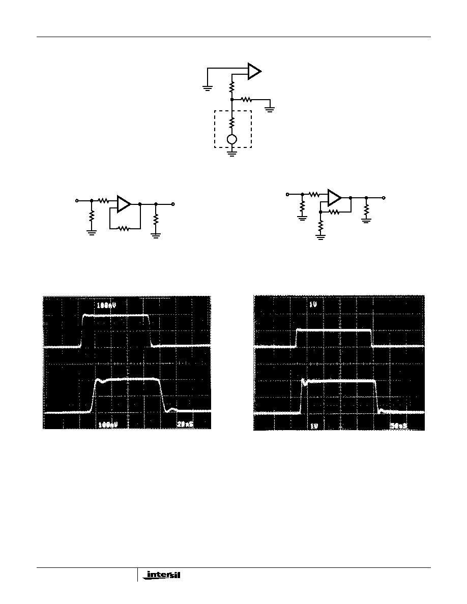
Test Circuits and Waveforms
FIGURE 1. TEST CIRCUIT FOR TRANSIMPEDANCE MEASUREMENTS
FIGURE 2. SMALL SIGNAL PULSE RESPONSE CIRCUIT
FIGURE 3. LARGE SIGNAL PULSE RESPONSE CIRCUIT
NOTE:
17. A series input resistor of
100
is recommended to limit input currents in case input signals are present before the HA5022 is powered up.
FIGURE 4. SMALL SIGNAL RESPONSE
FIGURE 5. LARGE SIGNAL RESPONSE
+
-
50
50
DUT
HP4195
NETWORK
ANALYZER
V
IN
V
OUT
R
L
R
F
, 1k
100
50
+
-
DUT
100
(NOTE 17)
V
IN
V
OUT
R
L
R
F
, 681
400
50
+
-
DUT
R
I
681
100
(NOTE 17)
Vertical Scale: V
IN
= 100mV/Div., V
OUT
= 100mV/Div.
Horizontal Scale: 20ns/Div.
Vertical Scale: V
IN
= 1V/Div., V
OUT
= 1V/Div.
Horizontal Scale: 50ns/Div.
HA5022
6
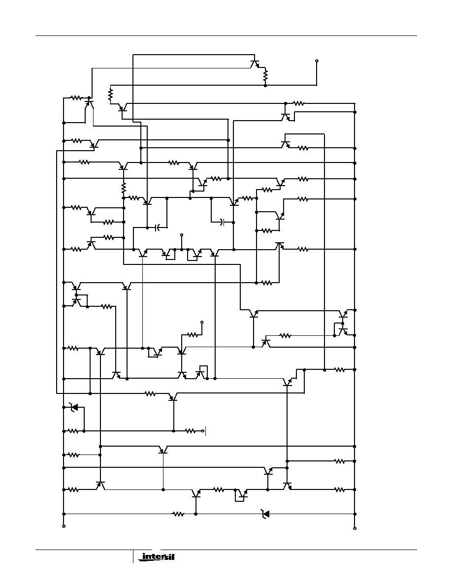
Schematic Diagram
(One Amplifier of Two)
R
2
800
R
5
2.5K
R
6
15K
D
2
Q
P2
R
1
60K
Q
N1
R
3
6K
Q
N2
D
1
Q
N3
Q
N4
R
4
800
R
7
15K
DIS
Q
N7
R
9
820
Q
P4
Q
N6
Q
P3
R
8
1.25K
Q
N5
+IN
Q
P7
R
13
1K
R
12
280
Q
P6
Q
N8
Q
P5
R
10
820
Q
N9
Q
N11
Q
N10
Q
P10
Q
P8
Q
P9
R
11
1K
R
14
280
Q
N14
R
16
400
R
22
280
Q
N16
R
17
280
R
18
280
Q
P11
R
15
400
R
19
400
Q
P14
Q
N12
Q
P12
-IN
Q
N13
Q
P13
C
2
R
23
400
R
26
200
R
24
140
R
20
140
Q
P15
C
1
Q
N17
R
25
20
Q
N18
R
25
140
R
21
140
R
26
200
Q
P16
R
27
200
R
33
2K
Q
P18
Q
N20
Q
P17
R
28
20
Q
N15
R
30
7
Q
N19
OUT
Q
N21
R
32
5
R
29
9.5
Q
P19
Q
P20
R
31
5
V+
V-
Q
P1
R
33
800
1.4pF
1.4pF
HA5022
7
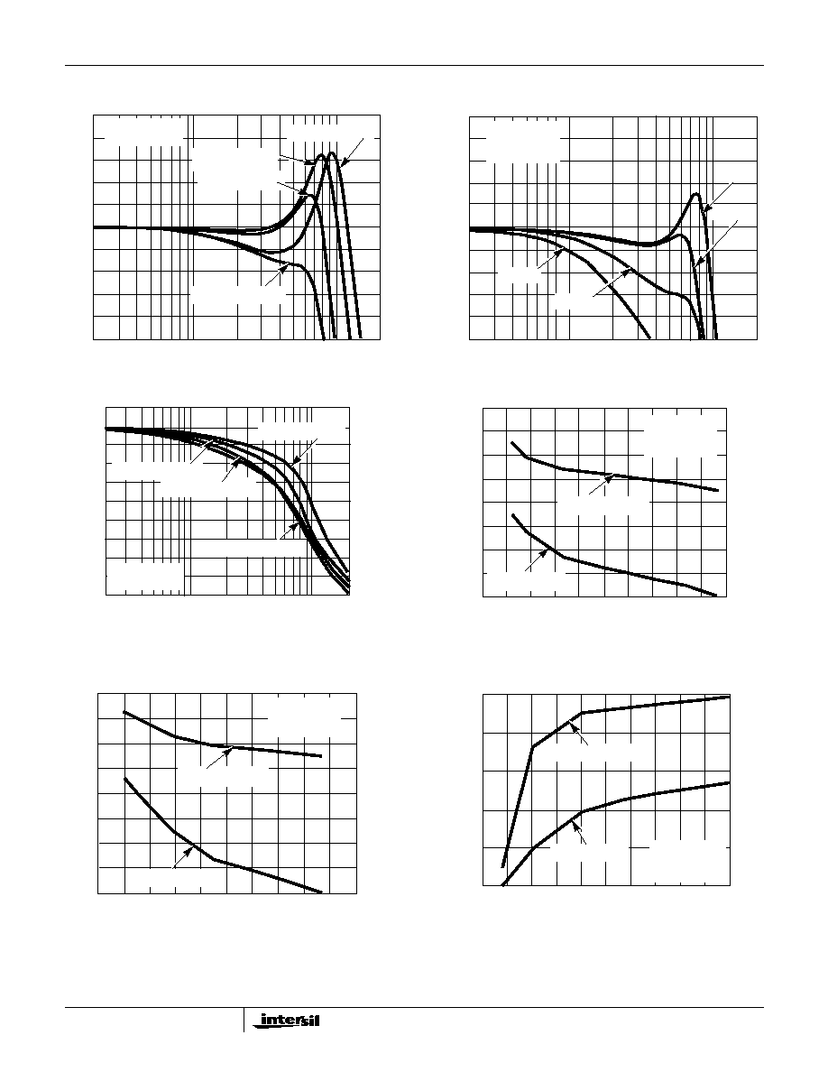
Application Information
Optimum Feedback Resistor
The plots of inverting and non-inverting frequency response,
see Figure 11 and Figure 12 in the Typical Performance
Curves section, illustrate the performance of the HA5022 in
various closed loop gain configurations. Although the
bandwidth dependency on closed loop gain isn't as severe
as that of a voltage feedback amplifier, there can be an
appreciable decrease in bandwidth at higher gains. This
decrease may be minimized by taking advantage of the
current feedback amplifier's unique relationship between
bandwidth and R
F
. All current feedback amplifiers require a
feedback resistor, even for unity gain applications, and R
F
, in
conjunction with the internal compensation capacitor, sets
the dominant pole of the frequency response. Thus, the
amplifier's bandwidth is inversely proportional to R
F
. The
HA5022 design is optimized for a 1000
R
F
at a gain of +1.
Decreasing R
F
in a unity gain application decreases stability,
resulting in excessive peaking and overshoot. At higher
gains the amplifier is more stable, so R
F
can be decreased
in a trade-off of stability for bandwidth.
The table below lists recommended R
F
values for various
gains, and the expected bandwidth.
PC Board Layout
The frequency response of this amplifier depends greatly on
the amount of care taken in designing the PC board. The
use of low inductance components such as chip resistors
and chip capacitors is strongly recommended. If leaded
components are used the leads must be kept short
especially for the power supply decoupling components and
those components connected to the inverting input.
Attention must be given to decoupling the power supplies. A
large value (10
µ
F) tantalum or electrolytic capacitor in
parallel with a small value (0.1
µ
F) chip capacitor works well
in most cases.
A ground plane is strongly recommended to control noise.
Care must also be taken to minimize the capacitance to
ground seen by the amplifier's inverting input (-IN). The
larger this capacitance, the worse the gain peaking, resulting
in pulse overshoot and possible instability. It is
recommended that the ground plane be removed under
traces connected to -IN, and that connections to -IN be kept
as short as possible to minimize the capacitance from this
node to ground.
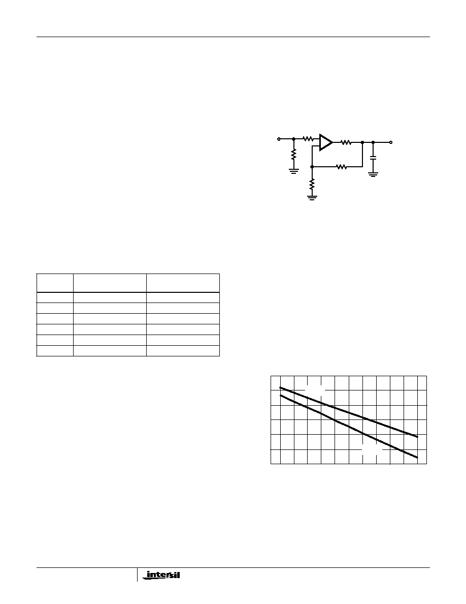
Driving Capacitive Loads
Capacitive loads will degrade the amplifier's phase margin
resulting in frequency response peaking and possible
oscillations. In most cases the oscillation can be avoided by
placing an isolation resistor (R) in series with the output as
shown in Figure 6.
The selection criteria for the isolation resistor is highly
dependent on the load, but 27
has been determined to be
a good starting value.
Power Dissipation Considerations
Due to the high supply current inherent in dual amplifiers,
care must be taken to insure that the maximum junction
temperature (T
J,
see Absolute Maximum Ratings) is not
exceeded. Figure 7 shows the maximum ambient
temperature versus supply voltage for the available package
styles (PDIP, SOIC). At V
S
=
±
5V quiescent operation both
package styles may be operated over the full industrial range
of -40
o
C to 85
o
C. It is recommended that thermal
calculations, which take into account output power, be
performed by the designer.
Enable/Disable Function
When enabled the amplifier functions as a normal current
feedback amplifier with all of the data in the electrical
specifications table being valid and applicable. When
GAIN
(A
CL
)
R
F
(
)
BANDWIDTH
(MHz)
-1
750
100
+1
1000
125
+2
681
95
+5
1000
52
+10
383
65
-10
750
22
V
IN
V
OUT
C
L
R
T
+
-
R
I
R
F
R
FIGURE 6. PLACEMENT OF THE OUTPUT ISOLATION
RESISTOR, R
100
140
130
120
110
100
90
80
5
7
9
11
13
15
MAX. AMBIENT TEMPERA
TURE
SUPPLY VOLTAGE (
±
V)
PDIP
SOIC
FIGURE 7. MAXIMUM OPERATING AMBIENT
TEMPERATURE vs SUPPLY VOLTAGE
HA5022
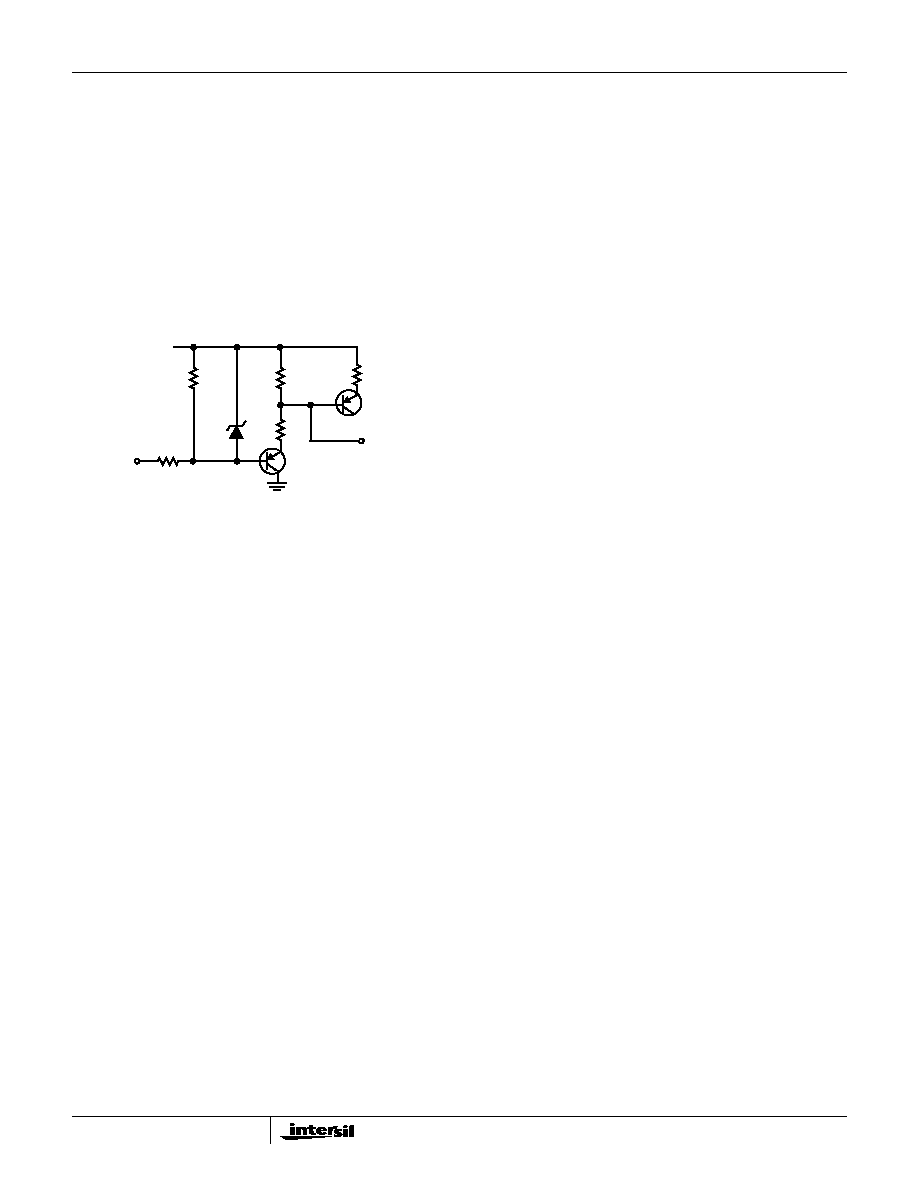
8
disabled the amplifier output assumes a true high
impedance state and the supply current is reduced
significantly.
The circuit shown in Figure 8 is a simplified schematic of the
enable/disable function. The large value resistors in series
with the DISABLE pin makes it appear as a current source to
the driver. When the driver pulls this pin low current flows out
of the pin and into the driver. This current, which may be as
large as 350
µ
A when external circuit and process variables
are at their extremes, is required to insure that point "A"
achieves the proper potential to disable the output. The
driver must have the compliance and capability of sinking all
of this current.
When V
CC
is +5V the DISABLE pin may be driven with a
dedicated TTL gate. The maximum low level output voltage
of the TTL gate, 0.4V, has enough compliance to insure that
the amplifier will always be disabled even though D
1
will not
turn on, and the TTL gate will sink enough current to keep
point "A" at its proper voltage. When V
CC
is greater than +5V
the DISABLE pin should be driven with an open collector
device that has a breakdown rating greater than V
CC
.
Referring to Figure 8, it can be seen that R
6
will act as a pull-
up resistor to +V
CC
if the DISABLE pin is left open. In those
cases where the enable/disable function is not required on
all circuits some circuits can be permanently enabled by
letting the DISABLE pin float. If a driver is used to set the
enable/disable level, be sure that the driver does not sink
more than 20
µ
A when the DISABLE pin is at a high level.
TTL gates, especially CMOS versions, do not violate this
criteria so it is permissible to control the enable/disable
function with TTL.
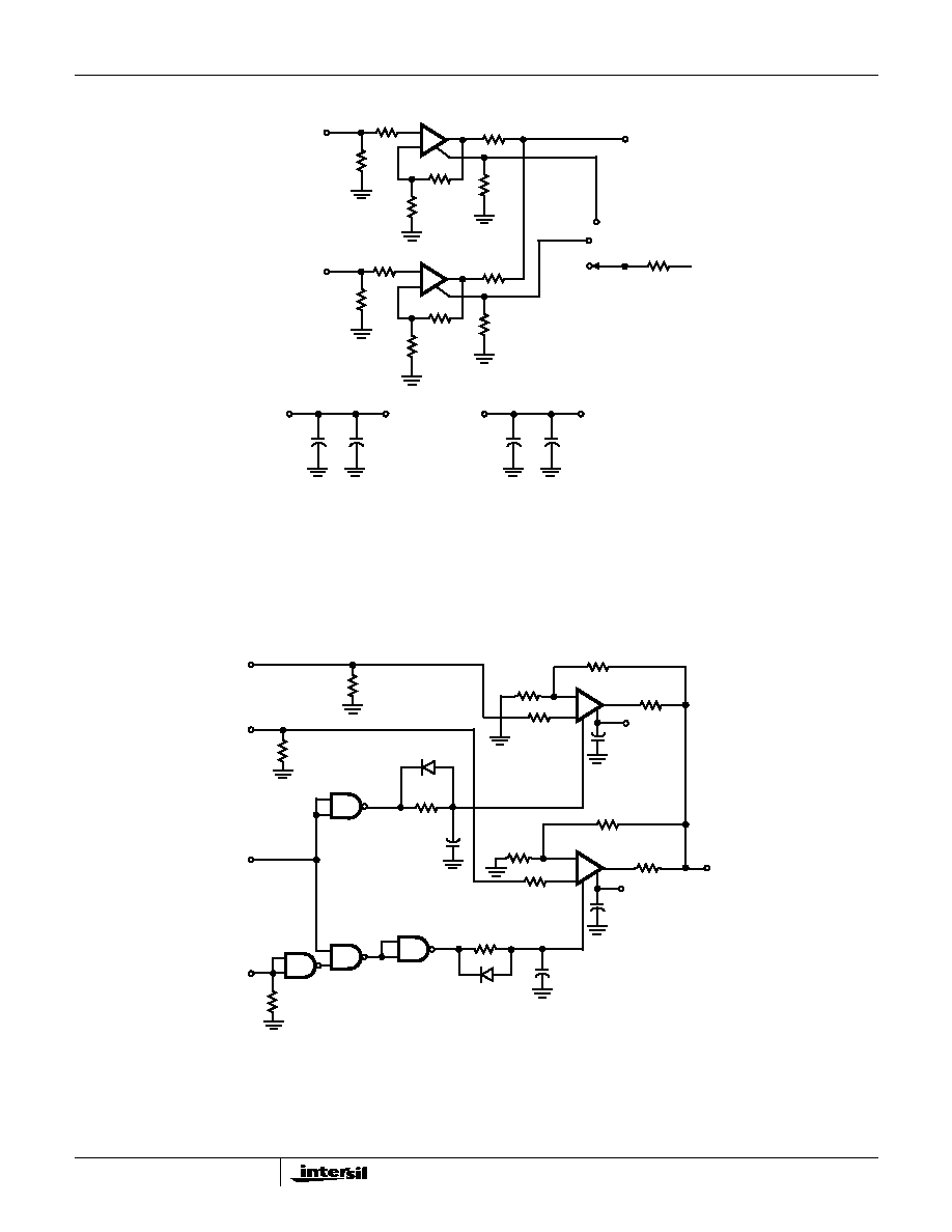
Typical Applications
Two Channel Video Multiplexer
Referring to the amplifier U
1A
in Figure 9, R
1
terminates the
cable in its characteristic impedance of 75
, and R
4
back
terminates the cable in its characteristic impedance. The
amplifier is set up in a gain configuration of +2 to yield an
overall network gain of +1 when driving a double terminated
cable. The value of R
3
can be changed if a different network
gain is desired. R
5
holds the disable pin at ground thus
inhibiting the amplifier until the switch, S
1
, is thrown to
position 1. At position 1 the switch pulls the disable pin up to
the plus supply rail thereby enabling the amplifier. Since all
of the actual signal switching takes place within the amplifier,
it's differential gain and phase parameters, which are 0.03%
and 0.03 degrees respectively, determine the circuit's
performance. The other circuit, U
1B
, operates in a similar
manner.
When the plus supply rail is 5V the disable pin can be driven
by a dedicated TTL gate as discussed earlier. If a multiplexer
IC or its equivalent is used to select channels its logic must
be break before make. When these conditions are satisfied
the HA5022 is often used as a remote video multiplexer, and
the multiplexer may be extended by adding more amplifier
ICs.
Low Impedance Multiplexer
Two common problems surface when you try to multiplex
multiple high speed signals into a low impedance source
such as an A/D converter. The first problem is the low source
impedance which tends to make amplifiers oscillate and
causes gain errors. The second problem is the multiplexer
which supplies no gain, introduces all kinds of distortion and
limits the frequency response. Using op amps which have an
enable/disable function, such as the HA5022, eliminates the
multiplexer problems because the external mux chip is not
needed, and the HA5022 can drive low impedance (large
capacitance) loads if a series isolation resistor is used.
Referring to Figure 10, both inputs are terminated in their
characteristic impedance; 75
is typical for video
applications. Since the drivers usually are terminated in their
characteristic impedance the input gain is 0.5, thus the
amplifiers, U
2
, are configured in a gain of +2 to set the circuit
gain equal to one. Resistors R
2
and R
3
determine the
amplifier gain, and if a different gain is desired R
2
should be
changed according to the equation G = (1 + R
3
/R
2
). R
3
sets
the frequency response of the amplifier so you should refer
to the manufacturers data sheet before changing its value.
R
5
, C
1
and D
1
are an asymmetrical charge/discharge time
circuit which configures U
1
as a break before make switch to
prevent both amplifiers from being active simultaneously. If
this design is extended to more channels the drive logic
must be designed to be break before make. R
4
is enclosed
in the feedback loop of the amplifier so that the large open
loop amplifier gain of U
2
will present the load with a small
closed loop output impedance while keeping the amplifier
stable for all values of load capacitance.
The circuit shown in Figure 10 was tested for the full range of
capacitor values with no oscillations being observed; thus,
problem one has been solved.The frequency and gain
characteristics of the circuit are now those of the amplifier
independent of any multiplexing action; thus, problem two
has been solved. The multiplexer transition time is
approximately 15
µ
s with the component values shown.
R
6
15K
R
7
15K
V+
ENABLE/DISABLE INPUT
D
1
Q
P3
R
8
Q
P18
A
R
33
R
10
FIGURE 8. SIMPLIFIED SCHEMATIC OF ENABLE/DISABLE
FUNCTION
HA5022
9
NOTES:
18. U
1
is HA5022.
19. All resistors in
.
20. S
1
is break before make.
21. Use ground plane.
FIGURE 9. TWO CHANNEL HIGH IMPEDANCE MULTIPLEXER
NOTES:
22. U
2
: HA5022.
23. U
1
: CD4011.
FIGURE 10. LOW IMPEDANCE MULTIPLEXER
VIDEO INPUT #1
VIDEO INPUT #2
R
1
75
R
3
681
R
2
681
R
4
75
R
5
2000
+
-
U
1A
1
2
3
16
U
1B
7
6
5
10
R
9
75
R
10
2000
R
7
681
R
8
681
R
6
75
+5V IN
+5V
0.1
µ
F
10
µ
F
-5V IN
-5V
0.1
µ
F
10
µ
F
+
+
1
R
11
100
VIDEO OUTPUT
TO 75
LOAD
+5V
S
1
2
3
ALL
OFF
100
(NOTE 17)
100
(NOTE 17)
+
-
INPUT B
+
-
-5V
+
-
+5V
INHIBIT
CHANNEL
SWITCH
INPUT A
R
1A
75
R
1B
75
D
1A
1N4148
U
1C
U
1A
U
1B
U
1D
R
6
100K
R
5A
2000
C
1A
0.047
µ
F
R
5B
2000
D
1B
1N4148
R
1A
681
1
2
3
4
16
R
3A
681
R
4A
27
0.01
µ
F
R
2B
681
R
4B
27
R
3B
681
0.01
µ
F
OUTPUT
7
6
5
13
10
U
2B
U
2A
C
1B
0.047
µ
F
100
(NOTE 17)
100
(NOTE 17)
HA5022
10
Typical Performance Curves
V
SUPPLY
=
±
5V, A
V
= +1, R
F
= 1k
, R
L
= 400
,
T
A
= 25
o
C, Unless Otherwise Specified
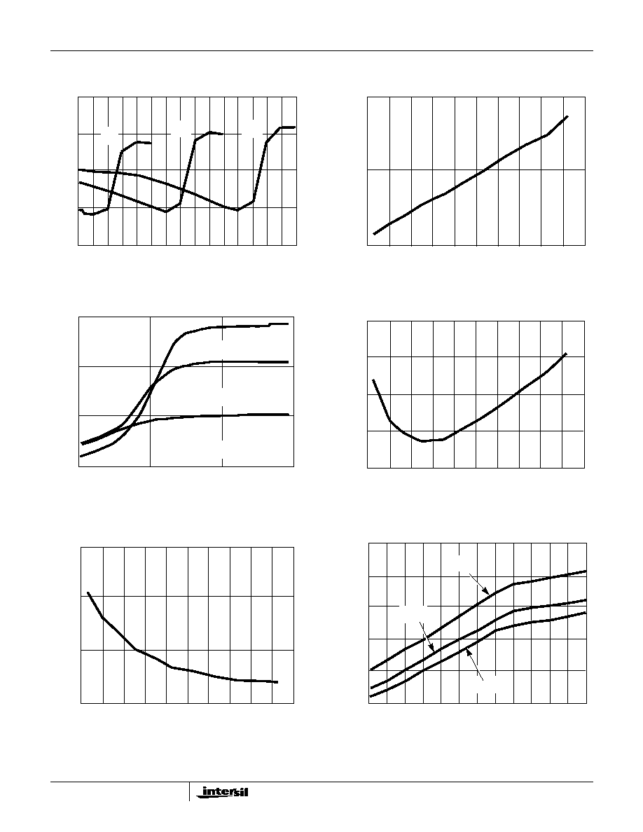
FIGURE 11. NON-INVERTING FREQUENCY RESPONSE
FIGURE 12. INVERTING FREQUENCY RESPONSE
FIGURE 13. PHASE RESPONSE AS A FUNCTION OF
FREQUENCY
FIGURE 14. BANDWIDTH AND GAIN PEAKING vs FEEDBACK
RESISTANCE
FIGURE 15. BANDWIDTH AND GAIN PEAKING vs FEEDBACK
RESISTANCE
FIGURE 16. BANDWIDTH AND GAIN PEAKING vs LOAD
RESISTANCE
5
4
3
2
1
0
-1
-2
-3
-4
-5
NORMALIZED GAIN (dB)
FREQUENCY (MHz)
2
10
100
200
V
OUT
= 0.2V
P-P
C
L
= 10pF
A
V
= +1, R
F
= 1k
A
V
= 2, R
F
= 681
A
V
= 5, R
F
= 1k
A
V
= 10, R
F
= 383
5
4
3
2
1
0
-1
-2
-3
-4
-5
2
10
100
200
FREQUENCY (MHz)
NORMALIZED GAIN (dB)
V
OUT
= 0.2V
P-P
C
L
= 10pF
R
F
= 750
A
V
= -1
A
V
= -2
A
V
= -10
A
V
= -5
FREQUENCY (MHz)
2
10
100
200
0
-45
-90
-135
-100
-225
-270
-315
-360
180
135
90
0
-45
-90
-135
45
-180
NONINVER
TING PHASE (DEGREES)
INVER
TING PHASE (DEGREES)
V
OUT
= 0.2V
P-P
C
L
= 10pF
A
V
= +10, R
F
= 383
A
V
= -10, R
F
= 750
A
V
= -1, R
F
= 750
A
V
= +1, R
F
= 1k
FEEDBACK RESISTOR (
)
500
700
900
1100
1300
1500
140
130
120
10
5
0
-3dB B
AND
WIDTH (MHz)
GAIN PEAKING (dB)
V
OUT
= 0.2V
P-P
C
L
= 10pF
-3dB BANDWIDTH
GAIN PEAKING
A
V
= +1
FEEDBACK RESISTOR (
)
-3dB B
AND
WIDTH (MHz)
GAIN PEAKING (dB)
100
95
90
0
350
500
650
800
950
1100
-3dB BANDWIDTH
GAIN PEAKING
V
OUT
= 0.2V
P-P
C
L
= 10pF
A
V
= +2
5
10
LOAD RESISTOR (
)
-3dB B
AND
WIDTH (MHz)
GAIN PEAKING (dB)
130
120
110
100
90
80
0
200
400
600
800
1000
6
4
2
0
V
OUT
= 0.2V
P-P
C
L
= 10pF
-3dB BANDWIDTH
GAIN PEAKING
A
V
= +1
HA5022

11
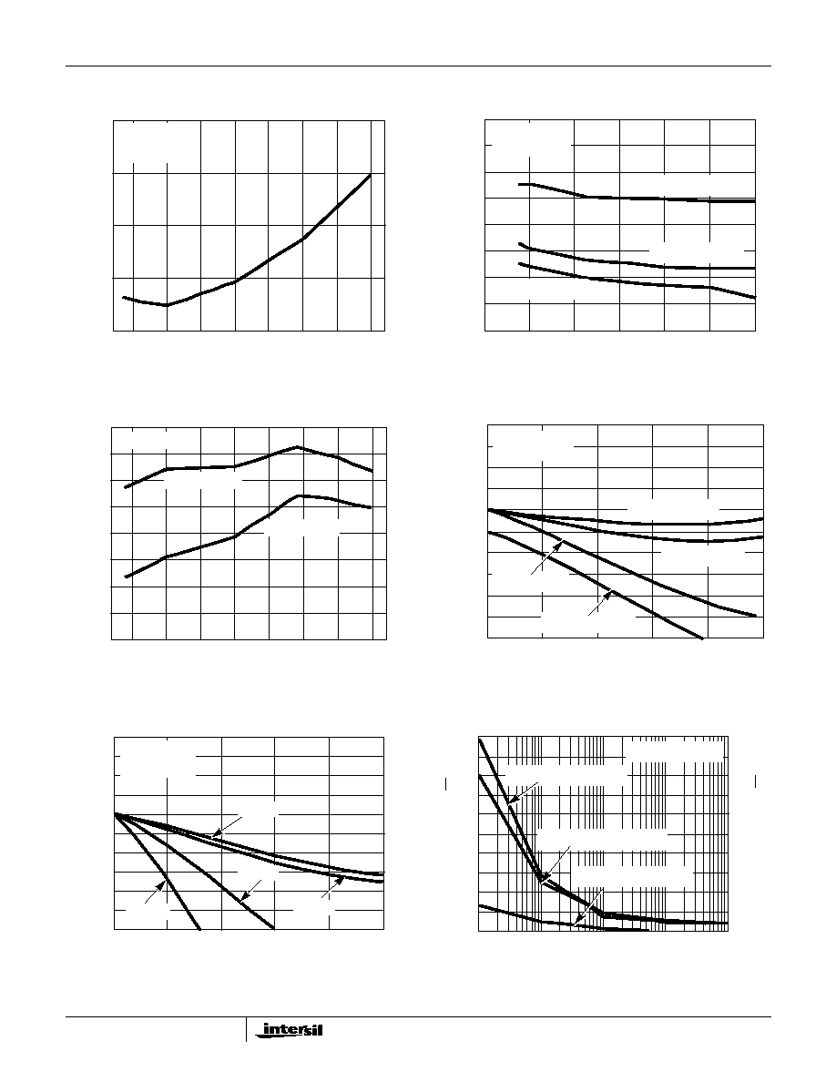
FIGURE 17. BANDWIDTH vs FEEDBACK RESISTANCE
FIGURE 18. SMALL SIGNAL OVERSHOOT vs LOAD
RESISTANCE
FIGURE 19. DIFFERENTIAL GAIN vs SUPPLY VOLTAGE
FIGURE 20. DIFFERENTIAL PHASE vs SUPPLY VOLTAGE
FIGURE 21. DISTORTION vs FREQUENCY
FIGURE 22. REJECTION RATIOS vs FREQUENCY
Typical Performance Curves
V
SUPPLY
=
±
5V, A
V
= +1, R
F
= 1k
, R
L
= 400
,
T
A
= 25
o
C, Unless Otherwise Specified (Continued)
80
60
40
20
0
200
350
500
650
800
950
-3dB B
AND
WIDTH (MHz)
FEEDBACK RESISTOR (
)
V
OUT
= 0.2V
P-P
C
L
= 10pF
A
V
= +10
LOAD RESISTANCE (
)
0
200
400
600
800
1000
16
6
0
O
VERSHOO
T (%)
V
OUT
= 0.1V
P-P
C
L
= 10pF
V
SUPPLY
=
±
5V, A
V
= +2
V
SUPPLY
=
±
15V, A
V
= +1
V
SUPPLY
=
±
5V, A
V
= +1
V
SUPPLY
=
±
15V, A
V
= +2
12
SUPPLY VOLTAGE (
±
V)
3
5
7
9
11
13
15
0.10
0.08
0.06
0.04
0.02
0.00
DIFFERENTIAL GAIN (%)
FREQUENCY = 3.58MHz
R
L
= 75
R
L
= 150
R
L
= 1k
0.08
0.06
0.04
0.02
0.00
3
5
7
9
11
13
15
SUPPLY VOLTAGE (
±
V)
DIFFERENTIAL PHASE (DEGREES)
R
L
= 1k
R
L
= 75
R
L
= 150
FREQUENCY = 3.58MHz
-40
-50
-60
-70
-80
-90
0.3
1
10
FREQUENCY (MHz)
DIST
OR
TION (dBc)
V
OUT
= 2.0V
P-P
C
L
= 30pF
HD3
HD2
3RD ORDER IMD
HD2
HD3
FREQUENCY (MHz)
0
-10
-20
-30
-40
-50
-60
-70
-80
REJECTION RA
TIO (dB)
0.001
0.01
0.1
1
10
30
A
V
= +1
CMRR
POSITIVE PSRR
NEGATIVE PSRR
HA5022
12
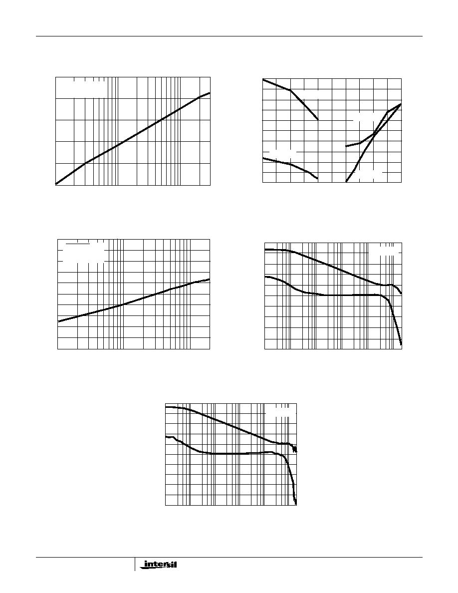
FIGURE 23. PROPAGATION DELAY vs TEMPERATURE
FIGURE 24. PROPAGATION DELAY vs SUPPLY VOLTAGE
FIGURE 25. SLEW RATE vs TEMPERATURE
FIGURE 26. NON-INVERTING GAIN FLATNESS vs FREQUENCY
FIGURE 27. INVERTING GAIN FLATNESS vs FREQUENCY
FIGURE 28. INPUT NOISE CHARACTERISTICS
Typical Performance Curves
V
SUPPLY
=
±
5V, A
V
= +1, R
F
= 1k
, R
L
= 400
,
T
A
= 25
o
C, Unless Otherwise Specified (Continued)
TEMPERATURE (
o
C)
-50
-25
0
25
50
75
100
125
8.0
7.5
7.0
6.5
6.0
PR
OP
A
G
A
TION DELA
Y (ns)
R
L
= 100
V
OUT
= 1.0V
P-P
A
V
= +1
SUPPLY VOLTAGE (
±
V)
PR
OP
A
G
A
TION DELA
Y (ns)
12
10
8
6
4
3
5
7
9
11
13
15
R
LOAD
= 100
V
OUT
= 1.0V
P-P
A
V
= +10, R
F
= 383
A
V
= +2, R
F
= 681
A
V
= +1, R
F
=1k
TEMPERATURE (
o
C)
-50
-25
0
25
50
75
100
125
500
450
400
350
300
250
200
150
100
SLEW RA
TE (V/
µ
s)
V
OUT
= 2V
P-P
+ SLEW RATE
- SLEW RATE
FREQUENCY (MHz)
5
10
15
20
25
30
0.8
0.6
0.4
0.2
0
-0.2
-0.4
-0.6
-0.8
-1.0
-1.2
NORMALIZED GAIN (dB)
V
OUT
= 0.2V
P-P
C
L
= 10pF
A
V
= +2, R
F
= 681
A
V
= +5, R
F
= 1k
A
V
= +1, R
F
= 1k
A
V
= +10, R
F
= 383
0.8
0.6
0.4
0.2
0
-0.2
-0.4
-0.6
-0.8
-1.0
-1.2
NORMALIZED GAIN (dB)
FREQUENCY (MHz)
5
10
15
20
25
30
V
OUT
= 0.2V
P-P
C
L
= 10pF
A
V
= -1
A
V
= -2
A
V
= -5
A
V
= -10
R
F
= 750
FREQUENCY (kHz)
0.01
0.1
1
10
100
V
O
L
T
A
GE NOISE (nV/
Hz)
CURRENT NOISE (pA/
Hz)
100
80
60
40
20
0
1000
800
600
400
200
0
A
V
= +10, R
F
= 383
-INPUT NOISE CURRENT
+INPUT NOISE CURRENT
INPUT NOISE VOLTAGE
HA5022

13
FIGURE 29. INPUT OFFSET VOLTAGE vs TEMPERATURE
FIGURE 30. +INPUT BIAS CURRENT vs TEMPERATURE
FIGURE 31. -INPUT BIAS CURRENT vs TEMPERATURE
FIGURE 32. TRANSIMPEDANCE vs TEMPERATURE
FIGURE 33. SUPPLY CURRENT vs SUPPLY VOLTAGE
FIGURE 34. REJECTION RATIO vs TEMPERATURE
Typical Performance Curves
V
SUPPLY
=
±
5V, A
V
= +1, R
F
= 1k
, R
L
= 400
,
T
A
= 25
o
C, Unless Otherwise Specified (Continued)
1.5
1.0
0.5
0.0
-60
-40
-20
0
40
60
80
100
120
140
20
V
IO
(mV)
TEMPERATURE (
o
C)
2
0
-2
-4
-60
-40
-20
0
40
60
80
100
120
140
20
BIAS CURRENT (
µ
A)
TEMPERATURE (
o
C)
22
20
18
16
-60
-40
-20
0
40
60
80
100
120
140
20
TEMPERATURE (
o
C)
BIAS CURRENT (
µ
A)
TEMPERATURE (
o
C)
4000
3000
2000
1000
TRANSIMPED
ANCE (k
)
-60
-40
-20
0
40
60
80
100
120
140
20
3
4
5
6
7
8
9
10
11
12
13
14
15
25
20
15
10
5
I
CC
(mA)
SUPPLY VOLTAGE (
±
V)
125
o
C
55
o
C
25
o
C
58
60
62
64
66
68
70
72
74
-100
-50
0
50
100
150
+PSRR
-PSRR
CMRR
200
250
TEMPERATURE (
o
C)
REJECTION RA
TIO (dB)
HA5022
14
FIGURE 35. SUPPLY CURRENT vs DISABLE INPUT VOLTAGE
FIGURE 36. OUTPUT SWING vs TEMPERATURE
FIGURE 37. OUTPUT SWING vs LOAD RESISTANCE
FIGURE 38. INPUT OFFSET VOLTAGE CHANGE BETWEEN
CHANNELS vs TEMPERATURE
FIGURE 39. INPUT BIAS CURRENT CHANGE BETWEEN
CHANNELS vs TEMPERATURE
FIGURE 40. DISABLE SUPPLY CURRENT vs SUPPLY VOLTAGE
Typical Performance Curves
V
SUPPLY
=
±
5V, A
V
= +1, R
F
= 1k
, R
L
= 400
,
T
A
= 25
o
C, Unless Otherwise Specified (Continued)
1
0
2
3
4
5
6
7
8
9
10 11 12 13 14 15
DISABLE INPUT VOLTAGE (V)
40
30
20
10
0
SUPPL
Y CURRENT (mA)
+5V
+10V
+15V
4.0
3.8
3.6
-60
-40
-20
0
40
60
80
100
120
140
20
TEMPERATURE (
o
C)
OUTPUT SWING (V)
0.01
0.10
1.00
10.00
30
20
10
0
V
OUT
(V
P-P
)
LOAD RESISTANCE (k
)
V
S
=
±
15V
V
S
=
±
10V
V
S
=
±
4.5V
-60
-40
-20
0
40
60
80
100
120
140
20
1.2
1.1
1.0
0.9
0.8
V
IO
(mV)
TEMPERATURE (
o
C)
-60
-40
-20
1.5
1.0
0.5
0.0
TEMPERATURE (
o
C)
BIAS CURRENT (
µ
A)
40
60
80
100
120
140
20
0
3
4
5
6
7
8
9
10
11
12
13
14
15
30
25
20
15
10
5
SUPPLY VOLTAGE (
±
V)
I
CC
(mA)
-55
o
C
25
o
C
125
o
C
HA5022
15
FIGURE 41. CHANNEL SEPARATION vs FREQUENCY
FIGURE 42. ENABLE/DISABLE TIME vs OUTPUT VOLTAGE
FIGURE 43. DISABLE FEEDTHROUGH vs FREQUENCY
FIGURE 44. TRANSIMPEDANCE vs FREQUENCY
FIGURE 45. TRANSIMPEDENCE vs FREQUENCY
Typical Performance Curves
V
SUPPLY
=
±
5V, A
V
= +1, R
F
= 1k
, R
L
= 400
,
T
A
= 25
o
C, Unless Otherwise Specified (Continued)
-30
-40
-50
-60
-70
-80
0.1
1
10
30
SEP
ARA
TION (dB)
FREQUENCY (MHz)
A
V
= +1
V
OUT
= 2V
P-P
DISABLE
ENABLE
ENABLE
DISABLE
ENABLE TIME (ns)
20
18
16
14
12
10
8
6
4
2
0
OUTPUT VOLTAGE (V)
-2.5 -2.0 -1.5
-1.0
-0.5
0
0.5
1.0
1.5
2.0
2.5
32
30
28
26
24
22
20
18
16
14
12
DISABLE TIME (
µ
s)
-20
-40
-50
-60
-70
-80
0.1
1
10
20
FEEDTHR
OUGH (dB)
FREQUENCY (MHz)
-30
-10
0
DISABLE = 0V
V
IN
= 5V
P-P
R
F
= 750
-135
-90
-45
0
45
90
135
180
10
1
0.1
0.01
0.001
0.001
0.01
0.1
1
10
100
PHASE ANGLE (DEGREES)
TRANSIMPED
ANCE (M
)
R
L
= 100
FREQUENCY (MHz)
-135
-90
-45
0
45
90
135
180
10
1
0.1
0.01
0.001
0.001
0.01
0.1
1
10
100
PHASE ANGLE (DEGREES)
R
L
= 400
FREQUENCY (MHz)
TRANSIMPED
ANCE (M
)
HA5022

16
All Intersil semiconductor products are manufactured, assembled and tested under ISO9000 quality systems certification.
Intersil semiconductor products are sold by description only. Intersil Corporation reserves the right to make changes in circuit design and/or specifications at any time with-
out notice. Accordingly, the reader is cautioned to verify that data sheets are current before placing orders. Information furnished by Intersil is believed to be accurate and
reliable. However, no responsibility is assumed by Intersil or its subsidiaries for its use; nor for any infringements of patents or other rights of third parties which may result
from its use. No license is granted by implication or otherwise under any patent or patent rights of Intersil or its subsidiaries.
For information regarding Intersil Corporation and its products, see web site http://www.intersil.com
Die Characteristics
DIE DIMENSIONS:
1650
µ
m x 2540
µ
m x 483
µ
m
METALLIZATION:
Type: Metal 1: AlCu (1%)
Thickness: Metal 1: 8k
≈
±
0.4k
≈
Type: Metal 2: AlCu (1%)
Thickness: Metal 2: 16k
≈
±
0.8k
≈
SUBSTRATE POTENTIAL (POWERED UP):
V-
PASSIVATION:
Type: Nitride
Thickness: 4k
≈
±
0.4k
≈
TRANSISTOR COUNT:
124
PROCESS:
High Frequency Bipolar Dielectric Isolation
Metallization Mask Layout
HA5022
-IN1
V+
OUT1
+IN2
DIS2
V-
NC
OUT2
-IN2
DIS1
+IN1
HA5022