 | –≠–ª–µ–∫—Ç—Ä–æ–Ω–Ω—ã–π –∫–æ–º–ø–æ–Ω–µ–Ω—Ç: HA-5101 | –°–∫–∞—á–∞—Ç—å:  PDF PDF  ZIP ZIP |

1
Æ
HA-5101
10MHz, Low Noise, Operational Amplifiers
The HA-5101 is a dielectrically isolated operational amplifier
featuring low noise, (3.0nV/
Hz at 1kHz).
DC characteristics of the HA-5101 assure accurate
performance. The 0.5mV offset voltage is externally adjust-
able and offset voltage drift is just 3
µ
V/
o
C. An offset current
of only 30nA reduces input current errors and an open loop
voltage gain of 1 x 10
6
V/V increases loop gain for low
distortion amplification.
The HA-5101 is ideal for audio applications, especially low-
level signal amplifiers such as microphone, tape head and
phono cartridge preamplifiers. Additionally, it is well suited
for low distortion oscillators, low noise function generators
and high Q filters.
Pinout
Features
∑ Low Noise . . . . . . . . . . . . . . . . . . . . . 3.0nV/
Hz at 1kHz
∑ Bandwidth . . . . . . . . . . . . . . . . . . . . . . . . . . . . . . . 10MHz
∑ Slew Rate. . . . . . . . . . . . . . . . . . . . . . . . . . . . . . . . 10V/
µ
s
∑ Low Offset Voltage Drift . . . . . . . . . . . . . . . . . . . . 3
µ
V/
o
C
∑ High Gain . . . . . . . . . . . . . . . . . . . . . . . . . . . . . 1 x 10
6
V/V
∑ High CMRR/PSRR . . . . . . . . . . . . . . . . . . . . . . . . . 100dB
∑ High Output Drive Capability . . . . . . . . . . . . . . . . . . 30mA
Applications
∑ High Quality Audio Preamplifiers
∑ High Q Active Filters
∑ Low Noise Function Generators
∑ Low Distortion Oscillators
∑ Low Noise Comparators
∑ For Further Design Ideas, See Application Note AN554
HA-5101(SOIC)
TOP VIEW
BAL
-IN
+IN
V-
2
3
4
1
V+
OUT
7
6
5
8
COMP
BAL
+
-
Ordering Information
PART NUMBER
(BRAND)
TEMP.
RANGE (
o
C)
PACKAGE
PKG.
NO.
HA9P5101-9
(H51019)
-40 to 85
8 Ld SOIC
M8.15
Data Sheet
April 2002
FN2905.4
CAUTION: These devices are sensitive to electrostatic discharge; follow proper IC Handling Procedures.
1-888-INTERSIL or 321-724-7143
|
Intersil (and design) is a registered trademark of Intersil Americas Inc.
Copyright © Intersil Americas Inc. 2002. All Rights Reserved

2
Schematic
R
24
Q
24
R
35
R
37
Q
37
R
22
Q
36
R
36
Q
35
Q
21
R
20
Q
20
Q
19A
Q
19B
R
19A
R
19B
R
11
R
10
R
25
R
23
Q
23
Q
25
Q
L41
Q
45
Q
44
Q
41
Q
11
Q
10
Q
12
R
12
Q
33
Q
31
Q
32
Q
46
Q
L1
Q
1A
Q
1B
Q
29
Q
38
Q
30
Q
43
Q
2B
Q
2A
Q
L2
Q
26
R
26
R
34
Q
5
Q
4
Q
3
Q
9
R
3A
Q
39
R
3B
R
27
Q
27
Q
47
R
60
R
28
Q
28
Q
16
Q
14
Q
15
OUTPUT
+IN
R
17A
Q
17
C
1
C
2
R
58
Q
8
Q
18
Q
48
Q
51
Q
42
Q
13
R
18
V-
BAL
BAL
R
15
Q
50
Q
49
R
4B
R
4A
Q
6
Q
34
V+
Q
7
-IN

3
Absolute Maximum Ratings
Thermal Information
Voltage Between V+ and V- Terminals . . . . . . . . . . . . . . . . . . . 40V
Differential Input Voltage . . . . . . . . . . . . . . . . . . . . . . . . . . . . . . . 7V
Input Voltage
. . . . . . . . . . . . . . . . . . . . . . . . . . . . . . . . . . . . . . ±
V
SUPPLY
Output Current . . . . . . . . . . . . . . . . . . . Full Short Circuit Protection
Operating Conditions
Temperature Range
HA-5101-9 . . . . . . . . . . . . . . . . . . . . . . . . . . . . . . . -40
o
C to 85
o
C
Thermal Resistance (Typical, Note 2)
JA
(
o
C/W)
JC
(
o
C/W)
SOIC Package . . . . . . . . . . . . . . . . . . .
160
N/A
Maximum Junction Temperature (Note 1) . . . . . . . . . . . . . . 150
o
C
Maximum Storage Temperature Range . . . . . . . . . -65
o
C to 150
o
C
Maximum Lead Temperature (Soldering 10s) . . . . . . . . . . . . 300
o
C
(Lead Tips Only)
CAUTION: Stresses above those listed in "Absolute Maximum Ratings" may cause permanent damage to the device. This is a stress only rating and operation of the
device at these or any other conditions above those indicated in the operational sections of this specification is not implied.
NOTES:
1. Maximum power dissipation, including output load, must be designed to maintain the maximum junction temperature below 150
o
C for the plastic
packages.
2.
JA
is measured with the component mounted on a low effective thermal conductivity test board in free air. See Tech Brief TB379
for details.
Electrical Specifications
V
SUPPLY
=
±
15V, R
S
= 100
,
R
L
= 2k
,
C
L
= 50pF, Unless Otherwise Specified
PARAMETER
TEST CONDITIONS
TEMP (
o
C)
MIN
TYP
MAX
UNITS
INPUT CHARACTERISTICS
Offset Voltage
25
-
0.5
3
mV
Full
-
-
4
mV
Offset Voltage Drift
Full
-
3
-
µ
V/
o
C
Bias Current
25
-
100
200
nA
Full
-
-
325
nA
Offset Current
25
-
30
75
nA
Full
-
-
125
nA
Input Resistance
25
-
500
-
k
Common Mode Range
Full
±
12
-
-
V
TRANSFER CHARACTERISTICS
Large Signal Voltage Gain
V
OUT
=
±
10V
25
-
1000
-
kV/V
Full
100
250
-
kV/V
Common Mode Rejection Ratio
V
CM
=
±
10V
Full
80
100
-
dB
Small Signal Bandwidth
A
V
= 1
25
-
10
-
MHz
Minimum Stable Gain
Full
1
-
-
V/V
OUTPUT CHARACTERISTICS
Output Voltage Swing
R
L
= 10k
Full
±
12
±
13
-
V
R
L
= 2k
Full
±
12
±
13
-
V
V
S
=
±
18V, R
L
= 600
25
±
15
-
-
V
Output Current (Note 3)
25
25
30
-
mA
Full Power Bandwidth (Note 4)
25
95
160
-
kHz
Output Resistance
25
-
110
-
Maximum Load Capacitance
25
-
800
-
pF
TRANSIENT RESPONSE (Note 5)
Rise Time
25
-
50
100
ns
Overshoot
25
-
20
35
%
4
Slew Rate
25
6
10
-
V/
µ
s
Settling Time (Note 6)
0.01%
-
-
2.6
-
µ
s
NOISE CHARACTERISTICS (Note 7)
Input Noise Voltage
f = 10Hz
25
-
5
7
nV/
Hz
f = 1kHz
25
-
3.0
4.0
nV/
Hz
Input Noise Current
f = 10Hz
25
-
4.0
9
pA/
Hz
f = 1kHz
-
0.6
2.5
pA/
Hz
Broadband Noise Voltage
f = DC To 30kHz
25
-
0.870
-
µ
V
RMS
POWER SUPPLY CHARACTERISTICS
Supply Current
Full
-
4
7
mA
Power Supply Rejection Ratio
V
S
=
±
5V
Full
80
100
-
dB
NOTES:
3. Output current is measured with V
OUT
=
±
15V with V
SUPPLY
=
±
18V.
4. Full power bandwidth is guaranteed by equation:
.
5. Refer to Test Circuits section of the data sheet.
6. Settling time is measured to 0.01% of final value for a 10V output step, and A
V
= -1.
7. The limits for these parameters are guaranteed based on lab characterization, and reflect lot-to-lot variation.
Electrical Specifications
V
SUPPLY
=
±
15V, R
S
= 100
,
R
L
= 2k
,
C
L
= 50pF, Unless Otherwise Specified (Continued)
PARAMETER
TEST CONDITIONS
TEMP (
o
C)
MIN
TYP
MAX
UNITS
Full power bandwidth
Slew Rate
2
VP
EAK
---------------------------
, V
PEAK
10V
=
=
Test Circuits and Waveforms
FIGURE 1. LARGE SIGNAL RESPONSE CIRCUIT
FIGURE 2. SMALL SIGNAL RESPONSE CIRCUIT
50pF
OUT
IN
2k
2k
1k
+
-
+
50pF
OUT
IN
2k
-

5
Application Information
Operation At
±
5V Supply
The HA-5101 performs well at V
S
=
±
5V exhibiting typical
characteristics as listed below:
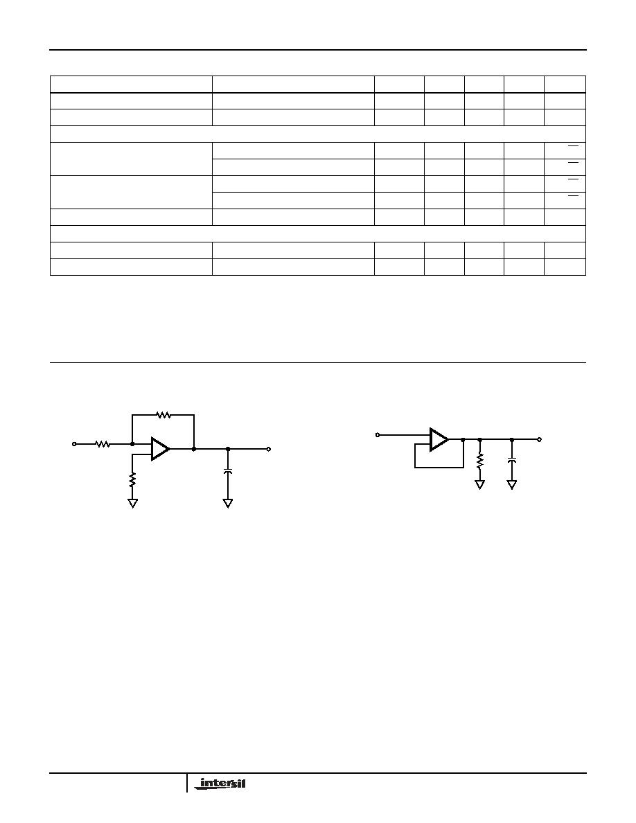
Offset Adjustment
The following is the recommended V
IO
adjust configuration:
NOTE: Proper decoupling is always recommended, 0.1
µ
F high quality
capacitor should be at or very near the device's supply pins.
Input Protection
The HA-5101 has built-in back-to-back protection diodes
which will limit the differential input voltage to approximately
Ch. 1 = 2.5V/Div.
Timebase = 1.00
µ
s/Div.
FIGURE 3. LARGE SIGNAL TRANSIENT RESPONSE
Ch. 1 = 50mV/Div.
Timebase = 100ns/Div.
FIGURE 4. SMALL SIGNAL TRANSIENT RESPONSE
NOTES:
8. A
V
= -1.
9. Feedback and summing resistors should be 0.1% matched.
10. Clipping diodes are optional, HP5082-2810 recommended.
FIGURE 5. SETTLING TIME CIRCUIT
Test Circuits and Waveforms
(Continued)
+5V
0V
-5V
+100mV
0V
-100mV
+
V
IN
2k
+15V
V
OUT
TO
OSCILLOSCOPE
2N4416
50pF
+15V
-15V
5k
2k
5k
(NOTE 9)
2k
(NOTE 9)
-
I
CC
. . . . . . . . . . . . . . . . . . . . . . . . . . . . . 3.7mA
V
IO
. . . . . . . . . . . . . . . . . . . . . . . . . . . . . 0.5mV
I
BIAS
. . . . . . . . . . . . . . . . . . . . . . . . . . . . 56nA
A
VOL
(V
O
=
±
3V) . . . . . . . . . . . . . . . . . . 106kV/V
V
OUT
. . . . . . . . . . . . . . . . . . . . . . . . . . . 3.7V
I
OUT
. . . . . . . . . . . . . . . . . . . . . . . . . . . . 13mA
CMRR (
V
CM
=
±
2.5V) . . . . . . . . . . . . . 90dB
PSRR (
V
S
= 0.5V) . . . . . . . . . . . . . . . . 90dB
Unity Gain Bandwidth . . . . . . . . . . . . . . 10MHz
Slew Rate. . . . . . . . . . . . . . . . . . . . . . . . 7V/
µ
s
+
+15V
(NOTE)
7
3
2
5
6
1
-15V
(NOTE)
RP
R
P
= 100k
4

6
7V. If the 5101 will be used in conditions where that voltage
may be exceeded, then current limiting resistors must be
used. No more than 25mA should be allowed to flow in the
HA-5101's input.
Comparator Circuit
Choose R
LIM
Such That:
Output Saturation
When an op amp is overdriven, output devices can saturate
and sometimes take a long time to recover. Saturation can
be avoided (sometimes) by using circuits such as:
If saturation cannot be avoided the HA-5101 recovers from a
25% overdrive in about 6.5
µ
s (see photos).
R
LIM
R
LIM
V
IN
V
IN
2
3
4
V-
6
7
V+
+
-
V
INMAX
7V
≠
(
)
25mA
---------------------------------------------
2R
LIM
+
R
1
R
2
V+
R
3
R
4
V-
V
SOURCE
-
IN
OUT
Top: Input
Bottom: Output, 5V/Div., 2
µ
s/Div.
Output is overdriven negative and recovers in 6
µ
s.
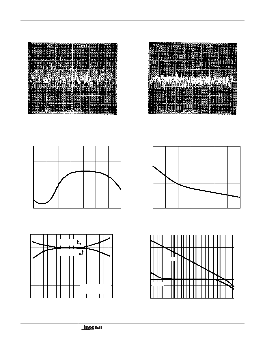
Typical Performance Curves
FIGURE 6. NOISE SPECTRUM
FIGURE 7. OFFSET VOLTAGE vs TEMPERATURE
FREQUENCY (Hz)
10
100
1K
10K
100K
0
1
2
3
4
5
6
7
8
I
N
PUT
NO
ISE CURRENT
(
p
A/
Hz
)
I
N
PUT
NO
I
SE VO
LT
AG
E (
n
V/
Hz
)
VOLTAGE
CURRENT
TEMPERATURE (
o
C)
125
100
75
50
25
0
-25
-50
0
500
1000
1500
O
F
F
SET VO
LT
AG
E (
µ
V)
7
A
V
= 25000 V
S
=
±
15V (2.25
µ
V
P-P
RTO)
PEAK-TO-PEAK NOISE 0.1Hz TO 10Hz
A
V
= 25000, V
S
=
±
15V (12.89mV
P-P
RTO)
PEAK-TO-PEAK TOTAL NOISE 0.1Hz TO 1MHz
FIGURE 8. INPUT OFFSET CURRENT vs TEMPERATURE
FIGURE 9. INPUT BIAS CURRENT vs TEMPERATURE
FIGURE 10. SLEW RATE/RISE TIME vs TEMPERATURE
FIGURE 11. OPEN-LOOP GAIN/PHASE vs FREQUENCY
Typical Performance Curves
(Continued)
0
20
-20
-40
-60
-55
-25
0
25
50
75
100
125
TEMPERATURE (
o
C)
INPUT
O
F
F
SET
CU
RRE
N
T
(
n
A)
150
200
100
50
0
-55
-25
0
25
50
75
100
125
TEMPERATURE (
o
C)
BIAS CU
RRE
N
T
(
n
A)
250
0.6
-60
-40
0
20
60
80
100
120
TEMPERATURE (
o
C)
40
-20
0.7
0.8
0.9
1.0
1.1
RISE TIME
SLEW RATE
R
L
= 2k
, C
L
= 50pF
V
S
=
±
15V
0.6
0.7
0.8
0.9
1.0
1.1
SL
E
W
RAT
E
(
N
ORM
A
L
I
Z
E
D)
R
I
S
E
TIM
E
(N
O
R
MA
L
I
Z
E
D
)
100M
FREQUENCY (Hz)
10M
1M
100K
10K
1K
100
10
0
20
40
60
80
100
120
140
0
45
90
135
180
PHAS
E SHI
F
T (
D
EG
RE
ES)
VO
L
T
AG
E G
A
I
N
(
d
B)
GAIN
PHASE

8
FIGURE 12. INPUT OFFSET WARMUP DRIFT vs TIME
(NORMALIZED TO ZERO FINAL VALUE)
(SIX REPRESENTATIVE UNITS)
FIGURE 13. SUPPLY CURRENT vs SUPPLY VOLTAGE
FIGURE 14. DC OPEN-LOOP VOLTAGE GAIN vs SUPPLY
VOLTAGE
FIGURE 15. SHORT CIRCUIT CURRENT vs TIME
Typical Performance Curves
(Continued)
450 500
TIME (SECONDS)
400
350
300
250
200
150
100
50
0
-30
-20
-10
0
10
20
30
O
F
F
S
E
T
CHANG
E (
µ
V)
T
A
= 25
o
C, V
S
=
±
15V
T
A
= 25
o
C
MAXIMUM
MINIMUM
TYPICAL
20
SUPPLY VOLTAGE (
±
V)
18
16
14
12
10
8
6
4
2
0
0
1
2
3
4
5
S
U
PPL
Y CURRENT
(
m
A)
15
10
18
5
SUPPLY VOLTAGE (
±
V)
10K
(80)
100K
(100)
1M
(120)
10M
(140)
V/V
(dB)
O
P
E
N
L
O
OP
V
O
L
T
AG
E
GAIN
160
140
120
100
80
60
40
20
0
0
10
20
30
40
50
60
T
A
= 25
o
C, V
S
=
±
15V
D
B
C
A
TIME (S)
OUT
P
UT
CURRENT
(
m
A)
V
IN
V
OUT
A
+15mV
±
15V
B
-15mV
±
15V
C
+15mV
0V
D
-15mV
0V

9
FIGURE 16. FREQUENCY RESPONSE
FIGURE 17. SETTLING WAVEFORM 1.5
µ
s/DIV.
FIGURE 18. CLOSED-LOOP GAIN vs FREQUENCY
FIGURE 19. REJECTION RATIOS vs FREQUENCY
FIGURE 20. +V
OUT
vs R
L
FIGURE 21. -V
OUT
vs R
L
Typical Performance Curves
(Continued)
V
s
=
±
15V, A
V
= 1V/V
R
L
= 2k
, C
L
= 50pF
100M
FREQUENCY (Hz)
10M
1M
100K
10K
-12
-9
-6
-3
0
3
6
-45
-90
-135
-180
P
H
A
S
E S
H
I
F
T
(
D
EG
R
E
ES
)
CL
OS
E
D
L
OOP
V
O
L
T
A
GE
GAI
N
(d
B)
-55
o
C
GAIN
-225
125
o
C
GAIN
-55
o
C
PHASE
125
o
C
PHASE
0
V
ERROR
2.65
µ
S
1mV
T
A
= 25
o
C, V
S
=
±
15V
R
L
= 2k
, C
L
= 50pF
100M
FREQUENCY (Hz)
10M
1M
100K
10K
-20
-10
0
10
20
30
40
GAI
N
(d
B)
A
V
= 10
A
V
= 100
A
V
= 1
T
A
= 25
o
C, V
s
=
±
15V
-PSRR/CMRR
+PSRR
FREQUENCY (Hz)
100
1K
10K
100K
1M
-120
-80
-100
-60
-40
REJ
E
CT
ION RAT
IO
(
d
B)
600
R
LOAD
(
)
500
400
300
200
9
10
11
12
13
14
100
+V
OU
T
(V
)
125
o
C
-55
o
C
25
o
C
V
SUPPLY
=
±
15V
R
LOAD
V
OUT
10k
100
-0.2V
+
-
600
R
LOAD
(
)
500
400
300
200
-14
-13
-12
-11
-10
-9
100
-
V
OU
T
(V
)
-55
o
C
25
o
C
V
SUPPLY
=
±
15V
R
LOAD
V
OUT
10k
100
+0.2V
+
-
125
o
C
-8
-7

10
All Intersil U.S. products are manufactured, assembled and tested utilizing ISO9000 quality systems.
Intersil Corporation's quality certifications can be viewed at www.intersil.com/design/quality
Intersil products are sold by description only. Intersil Corporation reserves the right to make changes in circuit design, software and/or specifications at any time without
notice. Accordingly, the reader is cautioned to verify that data sheets are current before placing orders. Information furnished by Intersil is believed to be accurate and
reliable. However, no responsibility is assumed by Intersil or its subsidiaries for its use; nor for any infringements of patents or other rights of third parties which may result
from its use. No license is granted by implication or otherwise under any patent or patent rights of Intersil or its subsidiaries.
For information regarding Intersil Corporation and its products, see www.intersil.com
Die Characteristics
SUBSTRATE POTENTIAL (Powered Up): V-
TRANSISTOR COUNT: 54
PROCESS: Bipolar Dielectric Isolation
Metallization Mask Layout
HA-5101
BAL
NC
-IN
+IN
OUT
V+
BAL
V-
HA-5101