 | –≠–ª–µ–∫—Ç—Ä–æ–Ω–Ω—ã–π –∫–æ–º–ø–æ–Ω–µ–Ω—Ç: HA-5137A | –°–∫–∞—á–∞—Ç—å:  PDF PDF  ZIP ZIP |
1
TM
File Number
2908.5
CAUTION: These devices are sensitive to electrostatic discharge; follow proper IC Handling Procedures.
1-888-INTERSIL or 321-724-7143
|
Intersil and Design is a trademark of Intersil Corporation.
|
Copyright
©
Intersil Corporation 2000
HA-5137A
63MHz, Ultra-Low Noise Precision
Operational Amplifier
The HA-5137 operational amplifier features an unparalleled
combination of precision DC and wideband high speed
characteristics. Utilizing the Intersil Dielectric Isolation
technology and advanced processing techniques, this
unique design unites low noise
precision
instrumentation performance with high speed (20V/
µ
s)
wideband capability.
This amplifier's impressive list of features include low V
OS
(10
µ
V), wide gain bandwidth (63MHz), high open loop gain
(1800V/mV), and high CMRR (126dB). Additionally, this
flexible device operates over a wide supply range (
±
5V to
±
20V) while consuming only 140mW of power.
Using the HA-5137 allows designers to minimize errors while
maximizing speed and bandwidth in applications requiring
gains greater than five.
This device is ideally suited for low level transducer signal
amplifier circuits. Other applications which can utilize the
HA-5137's qualities include instrumentation amplifiers, pulse
or RF amplifiers, audio preamplifiers, and signal conditioning
circuits.
This device can easily be used as a design enhancement by
directly replacing the 725, OP25, OP06, OP07, OP27 and
OP37 where gains are greater than five. For the military
grade product, refer to the HA-5137/883 data sheet.
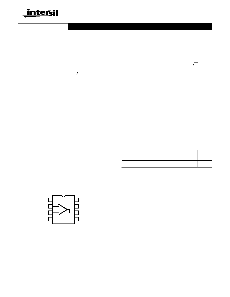
Pinout
HA-5137A
(CERDIP)
TOP VIEW
Features
∑ Slew Rate . . . . . . . . . . . . . . . . . . . . . . . . . . . . . . . . 20V/
µ
s
∑ Wide Gain Bandwidth (A
V
5) . . . . . . . . . . . . . . . 63MHz
∑ Low Noise. . . . . . . . . . . . . . . . . . . . . . .
at 1kHz
∑ Low V
OS
. . . . . . . . . . . . . . . . . . . . . . . . . . . . . . . . . . 10
µ
V
∑ High CMRR . . . . . . . . . . . . . . . . . . . . . . . . . . . . . . 126dB
∑ High Gain . . . . . . . . . . . . . . . . . . . . . . . . . . . . . 1800V/mV
Applications
∑ High Speed Signal Conditioners
∑ Wide Bandwidth Instrumentation Amplifiers
∑ Low Level Transducer Amplifiers
∑ Fast, Low Level Voltage Comparators
∑ Highest Quality Audio Preamplifiers
∑ Pulse/RF Amplifiers
∑ For Further Design Ideas See Application Note AN553
3nV
Hz
/
(
)
1
2
3
4
8
7
6
5
V+
OUT
BAL
V-
BAL
NC
-IN
+IN
-
+
Ordering Information
PART NUMBER
TEMP.
RANGE (
o
C)
PACKAGE
PKG.
NO.
HA7-5137A-5
0 to 75
8 Ld CERDIP
F8.3A
3nV/ Hz
Data Sheet
April 2000

2
Absolute Maximum Ratings
T
A
= 25
o
C
Thermal Information
Voltage Between V+ and V- Terminals. . . . . . . . . . . . . . . . . . . . 44V
Differential Input Voltage (Note 1) . . . . . . . . . . . . . . . . . . . . . . . 0.7V
Output Current . . . . . . . . . . . . . . . . . . . . Full Short Circuit Protection
Operating Conditions
Temperature Range
HA-5137A-5 . . . . . . . . . . . . . . . . . . . . . . . . . . . . . . . 0
o
C to 75
o
C
Thermal Resistance (Typical, Note 2)
JA
(
o
C/W)
JC
(
o
C/W)
CERDIP Package . . . . . . . . . . . . . . . . .
115
28
Maximum Junction Temperature (Hermetic Package) . . . . . . . 175
o
C
Maximum Storage Temperature Range . . . . . . . . . . -65
o
C to 150
o
C
Maximum Lead Temperature (Soldering 10s) . . . . . . . . . . . . 300
o
C
CAUTION: Stresses above those listed in "Absolute Maximum Ratings" may cause permanent damage to the device. This is a stress only rating and operation of the
device at these or any other conditions above those indicated in the operational sections of this specification is not implied.
NOTES:
1. For differential input voltages greater than 0.7V, the input current must be limited to 25mA to protect the back-to-back input diodes.
2.
JA
is measured with the component mounted on an evaluation PC board in free air.
Electrical Specifications
V
SUPPLY
=
±
15V, C
L
50pF, R
S
100
PARAMETER
TEST CONDITIONS
TEMP.
(
o
C)
MIN
TYP
MAX
UNITS
INPUT CHARACTERISTICS
Offset Voltage
25
-
10
25
µ
V
Full
-
30
60
µ
V
Average Offset Voltage Drift
Full
-
0.2
0.6
µ
V/
o
C
Bias Current
25
-
10
40
nA
Full
-
20
60
nA
Offset Current
25
-
7
35
nA
Full
-
15
50
nA
Common Mode Range
Full
±
10.3
±
11.5
-
V
Differential Input Resistance (Note 3)
25
1.5
6
-
M
Input Noise Voltage (Note 4)
0.1Hz to 10Hz
25
-
0.08
0.18
µ
V
P-P
Input Noise Voltage Density
(Note 5)
f = 10Hz
25
-
3.5
8.0
f = 100Hz
25
-
3.1
4.5
f = 1000Hz
25
-
3.0
3.8
Input Noise Current Density
(Note 5)
f = 10Hz
25
-
1.7
4.0
f = 100Hz
25
-
1.0
2.3
f = 1000Hz
25
-
0.4
0.6
TRANSFER CHARACTERISTICS
Large Signal Voltage Gain
R
L
= 2k
,
V
OUT
=
±
10V
25
1000
1800
-
V/mV
Full
600
1200
-
V/mV
Common Mode Rejection Ratio
V
CM
=
±
10V
Full
114
126
-
dB
Minimum Stable Gain
25
5
-
-
V/V
Gain-Bandwidth-Product
f = 10kHz
25
60
80
-
MHz
f = 1MHz
25
-
63
-
MHz
OUTPUT CHARACTERISTICS
Output Voltage Swing
R
L
= 600
25
±
10.0
±
11.5
-
V
R
L
= 2k
Full
±
11.7
±
13.8
-
V
Full Power Bandwidth (Note 6)
25
220
320
-
kHz
Output Resistance
Open Loop
25
-
70
-
Output Current
25
16.5
25
-
mA
TRANSIENT RESPONSE (Note 7)
Rise Time
25
-
-
100
ns
Slew Rate
V
OUT
=
±
3V
25
14
20
-
V/
µ
s
Settling Time
Note 8
25
-
1.0
-
µ
s
Overshoot
25
-
20
40
%
POWER SUPPLY CHARACTERISTICS
Supply Current
25
-
3.5
-
mA
Full
-
-
4.0
mA
nV/ Hz
nV/ Hz
nV/ Hz
pA/ Hz
pA/ Hz
pA/ Hz
HA-5137A

3
Power Supply Rejection Ratio
V
S
=
±
4V to
±
18V
Full
-
2
4
µ
V/V
NOTES:
3. This parameter value is based upon design calculations.
4. Refer to Typical Performance section of the data sheet.
5. The limits for this parameter are based on lab characterization, and reflect lot-to-lot variation.
6. Full power bandwidth guaranteed based on slew rate measurement using:
.
7. Refer to Test Circuits section of the data sheet.
8. Settling time is specified to 0.1% of final value for a 10V output step and A
V
= -5.
Electrical Specifications
V
SUPPLY
=
±
15V, C
L
50pF, R
S
100
(Continued)
PARAMETER
TEST CONDITIONS
TEMP.
(
o
C)
MIN
TYP
MAX
UNITS
FPBW
Slew Rate
2
V
PEAK
-----------------------------
=
Test Circuits and Waveforms
FIGURE 1. LARGE AND SMALL SIGNAL RESPONSE TEST CIRCUIT
Vertical Scale: Input = 1V/Div.
Output = 5V/Div.
Horizontal Scale: 1
µ
s/Div.
LARGE SIGNAL RESPONSE
Vertical Scale: Input = 20mV/Div.
Output = 100mV/Div.
Horizontal Scale: 100ns/Div.
SMALL SIGNAL RESPONSE
FIGURE 2. SETTLING TIME TEST CIRCUIT
IN
OUT
50pF
1.6k
400
+
-
IN
OUT
IN
OUT
OUT
-15V
+15V
50pF
IN
2N4416
5k
+15V
2k
1000
400
2k
TO
OSCILLOSCOPE
NOTES:
9. A
V
= -5.
10. Feedback and summing resistors should be
0.1% matched.
11. Clipping diodes are optional. HP5082-2810
recommended.
+
-
HA-5137A
4
Schematic Diagram
4
3
2
SUBSTRATE
+INPUT
Q
D60
R
5
R
6
Q
N24
Q
N25
Q
D59
Q
Z58
R
24
Q
N12
V-
R
4
R
14
Q
D8
Q
N45
C
7
D
1
R
15
Q
P37
Q
P55
Q
P56
Q
N19
R
1A
7
V+
R
25
R
1
Q
P32
1
8
BALANCE
R
16
Q
P35
Q
N46
Q
N47
R
2A
C
1
Q
N13
C
4
C
5
R
2
Q
N51
Q
N3
Q
D53
R
9
Q
N2
Q
P27
Q
N2A
C
6
Q
P36A
Q
P36
Q
D9
Q
N52
Q
N4
Q
D54
Q
P26
R
18
Q
N1A
Q
N1
Q
P40
Q
D41
Q
D22
Q
D23
Q
N42A
Q
N42
Q
N39
R
8
Q
N10
Q
N11
-INPUT
Q
N48
Q
N49
R
10
C
3
Q
N5
C
2
R
22
Q
N14
Q
N15
R
7
R
3
R
20
Q
P43
R
21
Q
P44
R
17
Q
P26
Q
P17
Q
P16
Q
N7
Q
N6
Q
N29
Q
N18
Q
P30
Q
D33
Q
D34
Q
N20
R
12
OUT-
R
13
Q
P21
6
PUT
R
23
Q
N50
Q
N57
Q
P38
R
19
HA-5137A
5
Application Information
NOTE:
Tested Offset Adjustment Range is |V
OS
+ 1mV| minimum referred to output. Typical range is
±
4mV with R
P
= 10k
.
FIGURE 3. SUGGESTED OFFSET VOLTAGE ADJUSTMENT
NOTE: Low resistances are preferred for low noise applications as a 1k
resistor has 4nV/
Hz of thermal noise. Total resistances of greater than
10k
on either input can reduce stability. In most high resistance applications, a few picofarads of capacitance across the feedback resistor will
improve stability.
FIGURE 4. SUGGESTED STABILITY CIRCUITS
Typical Performance Curves
Unless Otherwise Specified: T
A
= 25
o
C, V
SUPPLY
=
±
15V
FIGURE 5. OFFSET VOLTAGE DRIFT vs TEMPERATURE
FIGURE 6. NOISE CHARACTERISTICS
1
2
3
4
6
5
-
+
10K
R
P
V+
8
7
R
1
C
3
R
3
R
2
+
-
R
1
R
3
C
S
R
2
+
-
TEMPERATURE (
o
C)
OFFSET V
O
L
T
A
GE (
µ
V)
-60
-40
-20
0
20
40
60
80
120
100
-60
-50
-40
-30
-20
-10
0
10
30
20
V
S
=
±
15V, T
A
= 25
o
C
NOISE VOLTAGE
NOISE CURRENT
1M
100K
10K
1K
100
10
1
FREQUENCY (Hz)
0
2
4
6
8
10
12
NOISE VOLTAGE (nV/
Hz)
NOISE CURRENT (pA/
Hz)
0
1
2
3
4
5
6
HA-5137A