 | –≠–ª–µ–∫—Ç—Ä–æ–Ω–Ω—ã–π –∫–æ–º–ø–æ–Ω–µ–Ω—Ç: HA-5160 | –°–∫–∞—á–∞—Ç—å:  PDF PDF  ZIP ZIP |

1
HA-5160
100MHz, JFET Input, High Slew Rate,
Uncompensated, Operational Amplifier
The HA-5160 is a wideband, uncompensated, operational
amplifier with FET/Bipolar technologies and Dielectric
Isolation. This monolithic amplifier features superior high
frequency capabilities further enhanced by precision laser
trimming of the input stage to provide excellent input
characteristics. This device has excellent phase margin at a
closed loop gain of 10 without external compensation.
The HA-5160 offers a number of important advantages over
similar FET input op amps from other manufacturers. In
addition to superior bandwidth and settling characteristics,
the Intersil devices have nearly constant slew rate,
bandwidth, and settling characteristics over the operating
temperature range. This provides the user predictable
performance in applications where settling time, full power
bandwidth, closed loop bandwidth, or phase shift is critical.
Note also that Intersil specified all parameters at ambient
(rather than junction) temperature to provide the designer
meaningful data to predict actual operating performance.
Complementing the HA-5160's predictable and excellent
dynamic characteristics are very low input offset voltage, very
low input bias current, and a very high input impedance. This
ideal combination of features make these amplifiers most
suitable for precision, high speed, data acquisition system
designs and for a wide variety of signal conditioning
applications. The HA-5160 provides excellent performance for
applications which require both precision and high speed
performance.
Military version (/883) data sheets are available upon
request.
Pinout
HA-5160
(METAL CAN)
TOP VIEW
Features
∑ Wide Gain Bandwidth (A
V
10) . . . . . . . . . . . . . . 100MHz
∑ High Slew Rate. . . . . . . . . . . . . . . . . . . . . . . . . . . 120V/
µ
s
∑ Settling Time . . . . . . . . . . . . . . . . . . . . . . . . . . . . . 280ns
∑ Power Bandwidth . . . . . . . . . . . . . . . . . . . . . . . . . 1.9MHz
∑ Offset Voltage . . . . . . . . . . . . . . . . . . . . . . . . . . . . . 1.0mV
∑ Bias Current . . . . . . . . . . . . . . . . . . . . . . . . . . . . . . . 20pA
∑ Compensation Pin for Unity Gain Capability
Applications
∑ Video and RF Amplifiers
∑ Data Acquisition
∑ Pulse Amplifiers
∑ Precision Signal Generation
NOTE: Case connected to V-.
COMPENSATION
2
4
6
1
3
7
5
8
+IN
-IN
V-
OUT
NC
V+
NC
+
-
Ordering Information
PART NUMBER
TEMP.
RANGE (
o
C)
PACKAGE
PKG.
NO.
HA2-5160-2
-55 to 125
8 Pin Metal Can
T8.C
HA2-5160-5
0 to 75
8 Pin Metal Can
T8.C
Data Sheet
September 1998
File Number
2911.3
CAUTION: These devices are sensitive to electrostatic discharge; follow proper IC Handling Procedures.
1-888-INTERSIL or 321-724-7143
|
Copyright
©
Intersil Corporation 1999
2
H
Absolute Maximum Ratings
Thermal Information
Voltage Between V+ and V- . . . . . . . . . . . . . . . . . . . . . . . . . . . . 40V
Differential Input Voltage . . . . . . . . . . . . . . . . . . . . . . . . . . . . . . 40V
Peak Output Current . . . . . . . . . . . . . . . Full Short Circuit Protection
Operating conditions
Temperature Ranges
HA-5160-2 . . . . . . . . . . . . . . . . . . . . . . . . . . . . . . -55
o
C to 125
o
C
HA-5160-5 . . . . . . . . . . . . . . . . . . . . . . . . . . . . . . . . 0
o
C to 75
o
C
Supply Voltage Range (Typical) . . . . . . . . . . . . . . . . . .
±
7V to
±
18V
Thermal Resistance (Typical, Note 1)
JA
(
o
C/W)
JC
(
o
C/W)
Metal Can Package . . . . . . . . . . . . . . .
155
67
Maximum Junction Temperature . . . . . . . . . . . . . . . . . . . . . . . 175
o
C
Maximum Storage Temperature Range . . . . . . . . . . -65
o
C to 150
o
C
Maximum Lead Temperature (Soldering 10s) . . . . . . . . . . . . 300
o
C
Die Characteristics
Number of Transistors . . . . . . . . . . . . . . . . . . . . . . . . . . . . . . . . . 82
Substrate Potential (Powered Up) . . . . . . . . . . . . . . . . . . . . Floating
CAUTION: Stresses above those listed in "Absolute Maximum Ratings" may cause permanent damage to the device. This is a stress only rating and operation of the
device at these or any other conditions above those indicated in the operational sections of this specification is not implied.
NOTE:
1.
JA
is measured with the component mounted on an evaluation PC board in free air.
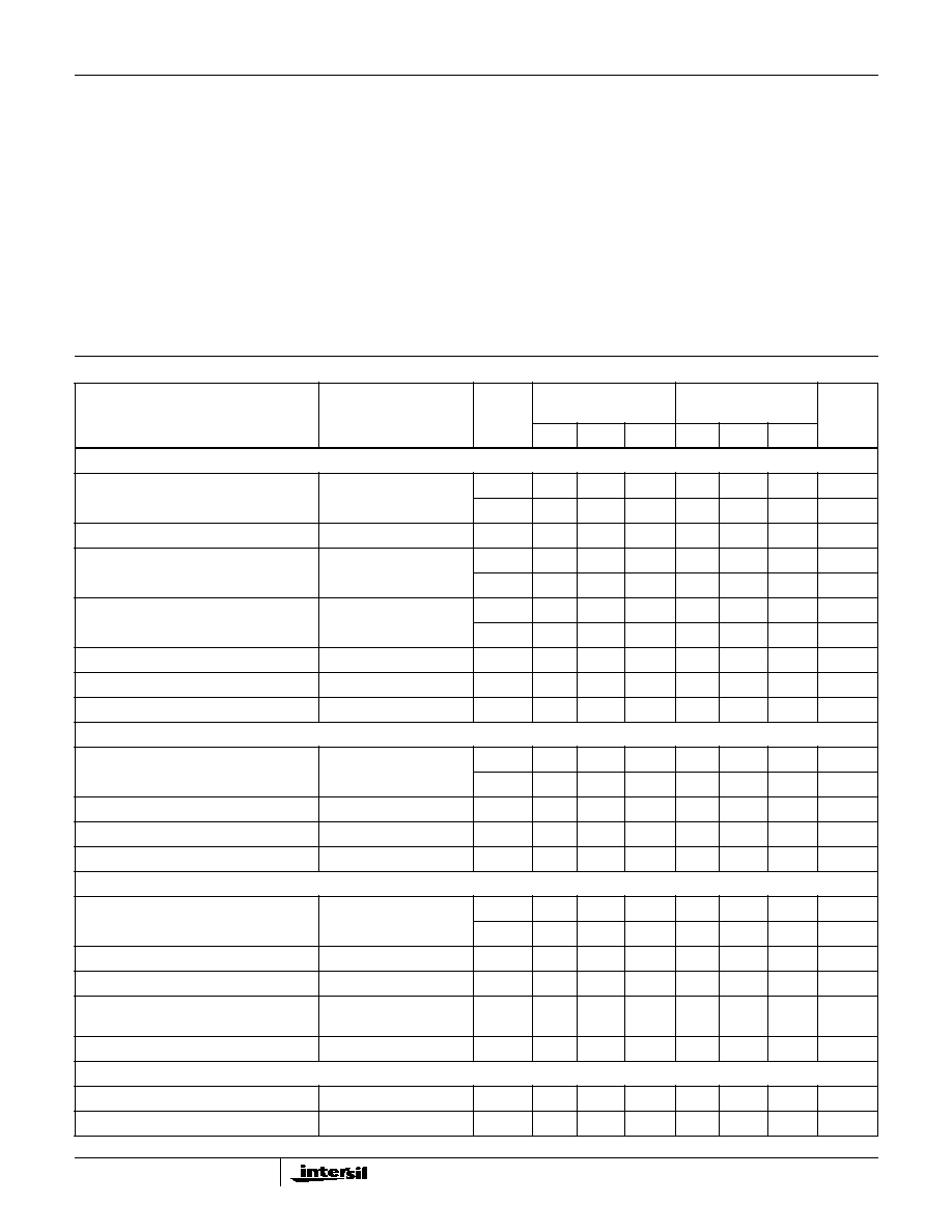
Electrical Specifications
V
SUPPLY
=
±
15V, Unless Otherwise Specified
PARAMETER
TEST CONDITIONS
TEMP.
(
o
C)
HA-5160-2
-55
o
C to 125
o
C
HA-5160-5
0
o
C to 75
o
C
UNITS
MIN
TYP
MAX
MIN
TYP
MAX
INPUT CHARACTERISTICS
Offset Voltage
25
-
1
3
-
1
3
mV
Full
-
3
5
-
3
5
mV
Offset Voltage Average Drift
Full
-
10
-
-
20
-
µ
V/
o
C
Bias Current
25
-
20
50
-
20
50
pA
Full
-
5
10
-
5
10
nA
Offset Current
25
-
2
10
-
2
10
pA
Full
-
2
5
-
2
5
nA
Input Capacitance
25
-
5
-
-
5
-
pF
Input Resistance
25
-
10
12
-
-
10
12
-
Common Mode Range
Full
±
10
±
11
-
±
10
±
11
-
V
TRANSFER CHARACTERISTICS
Large Signal Voltage Gain
V
OUT
=
±
10V,
R
L
= 2k
25
75
150
-
75
150
-
kV/V
Full
60
100
-
60
100
-
kV/V
Common Mode Rejection Ratio
V
CM
=
±
10V
Full
74
80
-
74
80
-
dB
Minimum Stable Gain
25
10
-
-
10
-
-
V/V
Gain Bandwidth Product
A
V
10
Full
-
100
-
-
100
-
MHz
OUTPUT CHARACTERISTICS
Output Voltage Swing
R
L
= 2k
25
±
10
±
11
-
±
10
±
11
-
V
Full
±
10
±
11
-
±
10
±
11
-
V
Output Current
V
OUT
=
±
10V
25
±
10
±
20
-
±
10
±
20
-
mA
Output Short Circuit Current
25
-
±
35
-
-
±
35
-
mA
Full Power Bandwidth (Note 2)
V
OUT
=
±
10V,
R
L
= 2k
25
1.6
1.9
-
1.6
1.9
-
MHz
Output Resistance
Open Loop
25
-
50
-
-
50
-
TRANSIENT RESPONSE (Note 3)
Rise Time
A
V
= +10
25
-
20
-
-
20
-
ns
Slew Rate
A
V
= +10
25
100
120
-
100
120
-
V/
µ
s
HA-5160
3
Settling Time (Note 4)
A
V
= -10
25
-
280
-
-
280
-
ns
POWER SUPPLY CHARACTERISTICS
Supply Current
Full
-
8
10
-
8
10
mA
Power Supply Rejection Ratio
V
S
=
±
10V to
±
20V
25
74
86
-
74
86
-
dB
NOTES:
2. Full Power Bandwidth guaranteed, based on slew rate measurement using:
.
3. Refer to Test circuits section of the data sheet.
4. Settling Time is measured to 0.2% of final value for a 10V output step.
Electrical Specifications
V
SUPPLY
=
±
15V, Unless Otherwise Specified (Continued)
PARAMETER
TEST CONDITIONS
TEMP.
(
o
C)
HA-5160-2
-55
o
C to 125
o
C
HA-5160-5
0
o
C to 75
o
C
UNITS
MIN
TYP
MAX
MIN
TYP
MAX
FPBW
Slew Rate
2
V
PEAK
-----------------------------
=
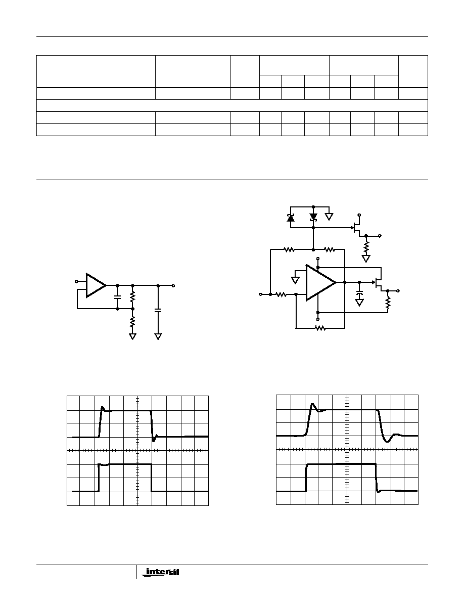
Test Circuits and Waveforms
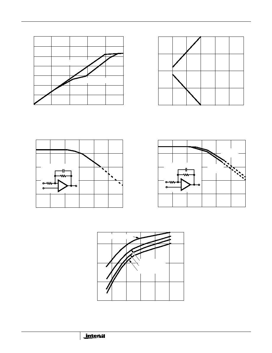
FIGURE 1. LARGE AND SMALL SIGNAL RESPONSE TEST CIRCUIT
NOTES:
5. A
V
= -10.
6. Feedback and summing resistors should be 0.1% matched.
7. Clipping diodes are optional. HP5082-2810 recommended.
FIGURE 2. SETTLING TIME TEST CIRCUIT
Vertical Scale: A = 0.5V/Div., B = 5V/Div.
Horizontal Scale: 500ns/Div.
LARGE SIGNAL RESPONSE
Vertical Scale: A = 10mV/Div., B = 100mV/Div.
Horizontal Scale: 100ns/Div.
SMALL SIGNAL RESPONSE
+
IN
OUT
50pF
1.8k
200
5pF
-
+
-15V
+15V
50pF
2N4416
5k
+15V
2k
200
2k
TO
OSCILLOSCOPE
500
V
OUT
V
IN
AUT
(NOTE 7)
3k
-
OUTPUT B
INPUT A
0V
0V
OUTPUT B
INPUT A
0V
0V
HA-5160
4
All Intersil semiconductor products are manufactured, assembled and tested under ISO9000 quality systems certification.
Intersil semiconductor products are sold by description only. Intersil Corporation reserves the right to make changes in circuit design and/or specifications at any time with-
out notice. Accordingly, the reader is cautioned to verify that data sheets are current before placing orders. Information furnished by Intersil is believed to be accurate and
reliable. However, no responsibility is assumed by Intersil or its subsidiaries for its use; nor for any infringements of patents or other rights of third parties which may result
from its use. No license is granted by implication or otherwise under any patent or patent rights of Intersil or its subsidiaries.
For information regarding Intersil Corporation and its products, see web site http://www.intersil.com
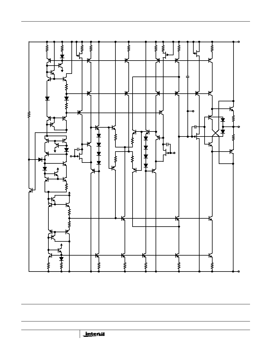
Schematic Diagram
R
100
Q
P51
Q
P49
D
83
D
53
V+
Q
N46
Q
N44
R
15
Q
N47
V+
Q
N78
Q
N45
Q
N76
Q
N77
R
52
R
53
Q
P80
Q
P79
Q
P81
V+
Q
N40
Q
N41
R
1
R
2
D
88
Q
N82
Q
P73
Q
P75
Q
P48
V-
Q
P50
D
52
R
8
R
9
D
87
Q
P43
Q
P42
Q
N84
V-
Q
N71
Q
N70
R
28
R
50
R
51
D
86
D
85
J
3
Q
P12
R
10
Q
P13
Q
P11
Q
N2
D
54
D
55
D
56
D
57
Q
P1
J
1
C
1
+IN
Q
P7
Q
N3
R
16
R
18
Q
P9
Q
P10
R
17
Q
P8
R
19
D
58
D
59
D
60
D
61
C
2
Q
P6
J
2
-IN
Q
N4
Q
N5
Q
P18
Q
N39
Q
N38
Q
N36
Q
N35
Q
N33
R
3
R
4
R
5
R
6
R
7
Q
N37
Q
N34
Q
N32
V-
R
11
R
12
R
24
R
13
J
4
J
6
R
14
Q
P27
Q
P23
Q
P16
Q
P14
Q
P17
Q
P15
Q
P24
Q
P25
Q
P26
COMP
C
4
C
3
V+
Q
N29
R
101
R
102
V
OUT
Q
P30
Q
N31
D
103
D
102
J
5
Q
P28
HA-5160

5
Application Information
Power Supply Decoupling
Although not absolutely necessary, it is recommended that
all power supply lines be decoupled with 0.01
µ
F ceramic
capacitors to ground. Decoupling capacitors should be
located as near to the amplifier terminals as possible.
Stability
The phase margin of the HA-5160 will be improved by
connecting a small capacitor (>10pF) between the output
and the inverting input of the device This small capacitor
compensates for the input capacitance of the FET.
Capacitive Loads
When driving large capacitive loads (>100pF), it is
suggested that a small resistor (
100
) be connected in
series with the output of the device and inside the feedback
loop.
Power Supply Minimum
The absolute supply minimum is
±
6V and the safe level is
±
7V.
Typical Applications
SUGGESTED COMPENSATION FOR UNITY GAIN STABILITY (NOTE)
FIGURE 3A. INVERTING UNITY GAIN CIRCUIT
FIGURE 3B. INVERTING UNITY GAIN PULSE RESPONSE
FIGURE 3. GAIN OF -1
NOTE: Values were determined experimentally for optimum speed and settling time.
FIGURE 4A. NONINVERTING UNITY GAIN CIRCUIT
FIGURE 4B. NONINVERTING UNITY GAIN PULSE RESPONSE
FIGURE 4. GAIN OF +1
2k
2k
+
IN
OUT
210
-
OUTPUT
Vertical Scale: 2V/Div.
Horizontal Scale: 500ns/Div.
IN
OUT
15pF
+
COMPENSATION
3
2
6
8
-
OUTPUT
Vertical Scale: 2V/Div.
Horizontal Scale: 500ns/Div.
HA-5160
6
Typical Performance Curves
FIGURE 5. INPUT OFFSET VOLTAGE AND BIAS CURRENT vs
TEMPERATURE
FIGURE 6. OPEN LOOP FREQUENCY RESPONSE
FIGURE 7. OUTPUT VOLTAGE SWING vs FREQUENCY
FIGURE 8. OPEN LOOP FREQUENCY RESPONSE FOR
VARIOUS COMPENSATION CAPACITANCES
FIGURE 9. INPUT NOISE VOLTAGE AND NOISE CURRENT vs
FREQUENCY
FIGURE 10. NORMALIZED AC PARAMETERS vs TEMPERATURE
TEMPERATURE (
o
C)
0
40
80
160
-1.50
-1.0
-0.50
+1.5
+2.0
BIAS CURRENT (pA)
120
-40
-80
+2.50
+0.0
+0.50
+1.0
OFFSET VOLTAGE
-2.0
1K
2K
3K
4K
OFFSET V
O
L
T
A
GE (mV)
BIAS CURRENT
FREQUENCY (Hz)
100K
80
OPEN LOOP V
O
L
T
A
GE GAIN (dB)
10
1M
40
10M
0
90
180
PHASE (DEGREES)
10K
1K
10
45
135
100M
100
70
100
110
-10
0
20
30
50
60
90
PHASE
GAIN
FREQUENCY (Hz)
100K
25
OUTPUT V
O
L
T
A
GE SWING (V
P-P
)
1M
5
15
10M
V
SUPPLY
=
±
20V
10K
1K
10
20
30
35
V
SUPPLY
=
±
15V
V
SUPPLY
=
±
10V
V
SUPPLY
=
±
7V
FREQUENCY (Hz)
100K
10
1M
10M
10K
1K
100M
100
80
OPEN LOOP V
O
L
T
A
GE GAIN (dB)
40
10
70
100
110
-10
0
20
30
50
60
90
0pF
50pF
100pF
300pF
FREQUENCY (Hz)
100K
10
SOURCE RESISTANCE = 100k
10K
1K
100
100
INPUT NOISE V
O
L
T
A
GE (nV/
Hz)
20
80
140
160
40
60
120
SOURCE RESISTANCE = 0
INPUT NOISE CURRENT
0.5
0.1
0.4
0.7
0.8
0.2
0.3
0.6
0
INPUT NOISE CURRENT (pA/
Hz)
TEMPERATURE (
o
C)
0
40
80
160
NORMALIZED P
ARAMETERS
120
-40
-80
0.6
0.7
1.0
1.1
0.9
0.8
0.5
0.4
REFERRED T
O
V
ALUES A
T
25
o
C
SLEW RATE
BANDWIDTH
BANDWIDTH
HA-5160
7
FIGURE 11. OUTPUT VOLTAGE SWING vs LOAD RESISTANCE
FIGURE 12. SETTLING TIME FOR VARIOUS OUTPUT STEP
VOLTAGES
FIGURE 13. COMMON MODE REJECTION RATIO vs FREQUENCY
FIGURE 14. POWER SUPPLY REJECTION RATIO vs FREQUENCY
FIGURE 15. POWER SUPPLY CURRENT vs TEMPERATURE
Typical Performance Curves
(Continued)
LOAD RESISTANCE (
)
200
400
600
1K
OUTPUT V
O
L
T
A
GE SWING (V)
800
0
6
10
14
12
8
4
2
NEGATIVE SWING
POSITIVE SWING
SETTLING TIME (ns)
100
400
600
OUTPUT V
O
L
T
A
GE STEP (V)
500
-10
0
+10
+5
300
200
0
-5
10mV
10mV
+
300pF
10
R
F
FREQUENCY (Hz)
1M
1
10K
1K
100
80
COMMON MODE REJECTION RA
TIO (dB)
0
60
100
20
40
100K
10
-
+
300pF
10
R
F
1M
1
10K
1K
100
80
PW
OER SUPPL
Y REJECTION RA
TIO (dB)
0
60
100
20
40
100K
10
FREQUENCY (Hz)
NEGATIVE
SUPPLY
POSITIVE
SUPPLY
-
TEMPERATURE (
o
C)
80
8.8
SUPPL
Y CURRENT (mA)
120
7.0
8.0
160
0
-80
7.5
8.5
40
-40
V
SUPPLY
=
±
15V
V
SUPPLY
=
±
10V
V
SUPPLY
=
±
7V
V
SUPPLY
=
±
20V
HA-5160