3-169
HA-5222/883
Dual, Low Noise, Wideband,
Precision Operational Amplifier
Description
The HA-5222/883 is a dual, high performance, dielectrically
isolated, monolithic op amp, featuring precision DC charac-
teristics while providing excellent AC characteristics.
Designed for audio, video, and other demanding applica-
tions, noise (3.3nV/
Hz at 1kHz typ), total harmonic distor-
tion (<0.005% typ), and DC errors are kept to a minimum.
The precision performance is shown by low offset voltage
(0.3mV typ), low bias currents (40nA typ), low offset cur-
rents (15nA typ), and high open loop gain (128dB typ). The
combination of these excellent DC characteristics with fast
settling time (0.4
µ
s typ) make the HA-5222/883 ideally
suited for precision signal conditioning.
The unique design of the HA-5222/883 gives this device out-
standing AC characteristics, including high unity gain band-
width (40MHz typ) and high slew rate (37V/
µ
s typ), not
normally associated with precision op amps. Other key spec-
ifications include high CMRR (95dB typ) and high PSRR
(100dB typ). The combination of these specifications will
allow the HA-5222/883 to be used in RF signal conditioning
as well as video amplifiers.
Ordering Information
PART
NUMBER
TEMPERATURE
RANGE
PACKAGE
HA7-5222/883
-55
o
C to +125
o
C
8 Lead CerDIP
Features
∑ This Circuit is Processed in Accordance to MIL-STD-
883 and is Fully Conformant Under the Provisions of
Paragraph 1.2.1.
∑ Gain Bandwidth Product . . . . . . . . . . . . . 100MHz (Min)
∑ Unity Gain Bandwidth . . . . . . . . . . . . . . . . 30MHz (Min)
40MHz (Typ)
∑ High Slew Rate . . . . . . . . . . . . . . . . . . . . . . 25V/
µ
s (Min)
37V/
µ
s (Typ)
∑ Low Offset Voltage. . . . . . . . . . . . . . . . . . 0.75mV (Max)
0.30mV (Typ)
∑ High Open Loop Gain . . . . . . . . . . . . . . . . . 106dB (Min)
128dB (Typ)
∑ Channel Separation (at 10kHz) . . . . . . . . . . 110dB (Typ)
∑ Low Voltage Noise (at 1kHz) . . . . . . . . 5.9nV/
Hz (Max)
3.3nV/
Hz (Typ)
∑ Low Current Noise (at 1kHz) . . . . . . . . 2.7pA/
Hz (Max)
1.3pA/
Hz (Typ)
∑ High Output Current . . . . . . . . . . . . . . . . .
±
30mA (Min)
±
56mA (Typ)
∑ Low Supply Current (per Op Amp.) . . . . . . 10mA (Max)
8mA (Typ)
Applications
∑ Precision Test Systems
∑ Active Filtering
∑ Small Signal Video
∑ Accurate Signal Processing
∑ RF Signal Conditioning
January 1996
Spec Number
511062-883
File Number
3717.1
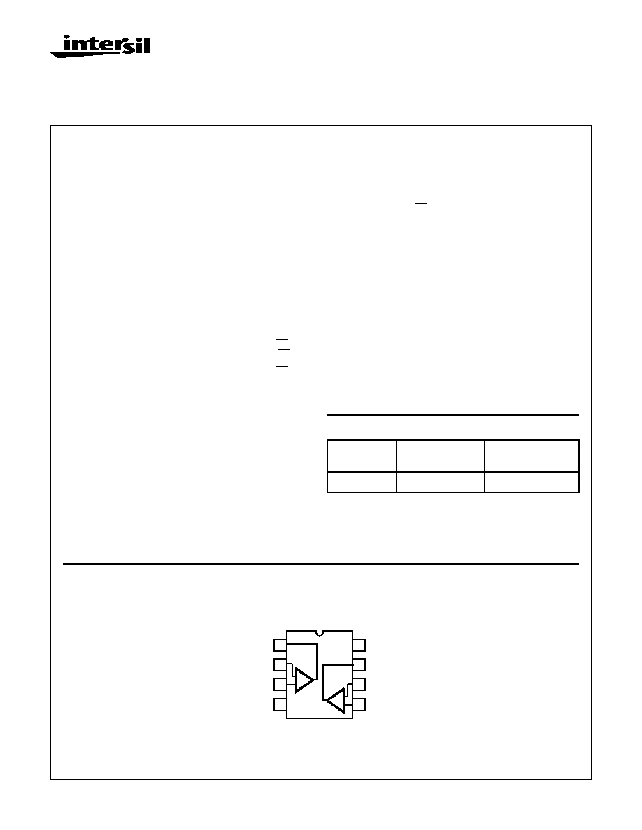
Pinout
HA-5222/883
(CERDIP)
TOP VIEW
2
3
4
1
7
6
5
8
+
+
OUT1
OUT2
1
2
+IN2
-IN2
V-
V+
+IN1
-IN1
-
-
CAUTION: These devices are sensitive to electrostatic discharge; follow proper IC Handling Procedures.
1-888-INTERSIL or 321-724-7143
|
Copyright
©
Intersil Corporation 1999
3-170
Specifications HA-5222/883
Absolute Maximum Ratings
Thermal Information (Typical)
Voltage Between V+ and V- Terminals . . . . . . . . . . . . . . . . . . . . 36V
Differential Input Voltage. . . . . . . . . . . . . . . . . . . . . . . . . . . . . . . . 5V
Voltage at Either Input Terminal . . . . . . . . . . . . . . . . . . . . . . V+ to V-
Peak Output Current (Pulsed at 1ms, 10% Duty Cycle) . . . . . 100mA
Continuous Output Current. . . . . . . . . . . . . . Short Circuit Protected
Junction Temperature . . . . . . . . . . . . . . . . . . . . . . . . . . . . . . +175
o
C
Storage Temperature Range . . . . . . . . . . . . . . . . . -65
o
C to +150
o
C
ESD Rating. . . . . . . . . . . . . . . . . . . . . . . . . . . . . . . . . . . . . . <2000V
Lead Temperature (Soldering 10s) . . . . . . . . . . . . . . . . . . . . +300
o
C
Thermal Resistance
JA
JC
CerDIP Package . . . . . . . . . . . . . . . . . . .
96
o
C/W
16
o
C/W
Package Power Dissipation Limit at +75
o
C
CerDIP Package . . . . . . . . . . . . . . . . . . . . . . . . . . . . . . . . . 1.04W
Package Power Dissipation Derating Factor Above +75
o
C
CerDIP Package . . . . . . . . . . . . . . . . . . . . . . . . . . . . . 10.4mW/
o
C
CAUTION: Stresses above those listed in "Absolute Maximum Ratings" may cause permanent damage to the device. This is a stress only rating and operation
of the device at these or any other conditions above those indicated in the operational sections of this specification is not implied.
Operating Conditions
Operating Temperature Range . . . . . . . . . . . . . . . . -55
o
C to +125
o
C
Operating Supply Voltage
. . . . . . . . . . . . . . . . . . . . . . . . . . ±
5V to
±
15V
V
INCM
1/2 (V+ - V-)
R
L
1k
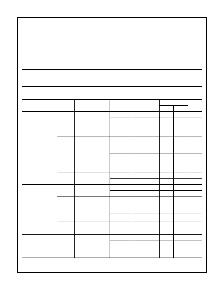
TABLE 1. DC ELECTRICAL PERFORMANCE CHARACTERISTICS
Device Tested at: V
SUPPLY
=
±
15V, R
LOAD
= 1k
, V
OUT
= 0V, Unless Otherwise Specified.
PARAMETERS
SYMBOL
CONDITIONS
GROUP A
SUBGROUPS
TEMPERATURE
LIMITS
UNITS
MIN
MAX
Input Offset Voltage
V
IO
V
CM
= 0V
1
+25
o
C
-0.75
0.75
mV
2, 3
+125
o
C, -55
o
C
-1.5
1.5
mV
Input Bias Current
+I
B
V
CM
= 0V,
+R
S
= 100.1k
,
-R
S
= 100
1
+25
o
C
-80
80
nA
2, 3
+125
o
C, -55
o
C
-200
200
nA
-I
B
V
CM
= 0V, +R
S
= 100
,
-R
S
= 100.1k
1
+25
o
C
-80
80
nA
2, 3
+125
o
C, -55
o
C
-200
200
nA
Input Offset Current
I
IO
V
CM
= 0V,
+R
S
= 100.1k
,
-R
S
= 100.1k
1
+25
o
C
-50
50
nA
2, 3
+125
o
C, -55
o
C
-150
150
nA
Common Mode Range
+CMR
V+ = +3V, V- = -27V
1
+25
o
C
12
-
V
2, 3
+125
o
C, -55
o
C
12
-
V
-CMR
V+ = +27V, V- = -3V
1
+25
o
C
-
-12
V
2, 3
+125
o
C, -55
o
C
-
-12
V
Large Signal Voltage
Gain
+A
VOL
V
OUT
= 0V and +10V
4
+25
o
C
106
-
dB
5, 6
+125
o
C, -55
o
C
100
-
dB
-A
VOL
V
OUT
= 0V and -10V
4
+25
o
C
106
-
dB
5, 6
+125
o
C, -55
o
C
100
-
dB
Common Mode
Rejection Ratio
+CMRR
V
CM
= +10V,
V+ = +5V, V- = -25V,
V
OUT
= -10V
1
+25
o
C
88
-
dB
2, 3
+125
o
C, -55
o
C
86
-
dB
-CMRR
V
CM
= -10V,
V+ = +25V, V- = -5V,
V
OUT
= +10V
1
+25
o
C
88
-
dB
2, 3
+125
o
C, -55
o
C
86
-
dB
Output Voltage Swing
+V
OUT
R
L
= 1k
4
+25
o
C
12.0
-
V
5, 6
+125
o
C, -55
o
C
11.5
-
V
-V
OUT
R
L
= 1k
4
+25
o
C
-
-12.0
V
5, 6
+125
o
C, -55
o
C
-
-11.5
V
Spec Number
511062-883
3-171
Spec Number
511062-883
Specifications HA-5222/883
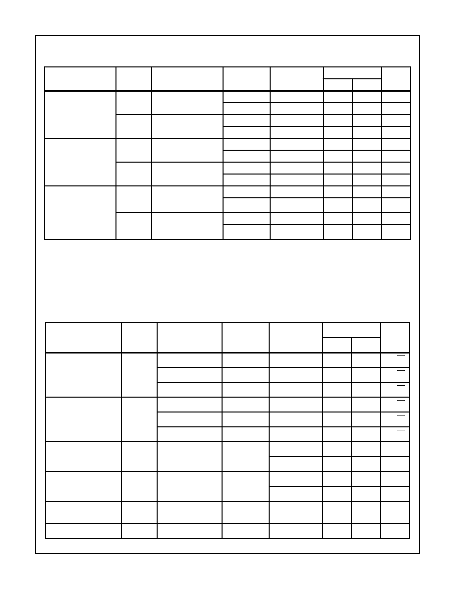
Output Current
+I
OUT
V
OUT
= +10V, R
L
= 1k
4
+25
o
C
30
-
mA
5, 6
+125
o
C, -55
o
C
30
-
mA
-I
OUT
V
OUT
= -10V, R
L
= 1k
4
+25
o
C
-
-30
mA
5, 6
+125
o
C, -55
o
C
-
-30
mA
Quiescent Power Supply
Current
+I
CC
V
OUT
= 0V, I
OUT
= 0mA
1
+25
o
C
-
20
mA
2, 3
+125
o
C, -55
o
C
-
22
mA
-I
CC
V
OUT
= 0V, I
OUT
= 0mA
1
+25
o
C
-20
-
mA
2, 3
+125
o
C, -55
o
C
-22
-
mA
Power Supply
Rejection Ratio
+PSRR
V
SUP
= 10V,
V+ = +20V, V- = -15V,
V+ = +10V, V- = -15V
1
+25
o
C
90
-
dB
2, 3
+125
o
C, -55
o
C
86
-
dB
-PSRR
V
SUP
= 10V,
V+ = +15V, V- = -20V,
V+ = +15V, V- = -10V
1
+25
o
C
90
-
dB
2, 3
+125
o
C, -55
o
C
86
-
dB
TABLE 2. AC ELECTRICAL PERFORMANCE CHARACTERISTICS
Table 2 Intentionally Left Blank. See AC Specifications in Table 3.
TABLE 3. ELECTRICAL PERFORMANCE CHARACTERISTIC
Device Characterized at: V
SUPPLY
=
±
15V, R
LOAD
= 1k
, Unless Otherwise Specified.
PARAMETERS
SYMBOL
CONDITIONS
NOTES
TEMPERATURE
LIMITS
UNITS
MIN
MAX
Input Noise Voltage
Density
E
N
R
S
= 0
, f
O
= 10Hz
1, 5
+25
o
C
-
16.0
nV
/
Hz
R
S
= 0
, f
O
= 100Hz
1, 5
+25
o
C
-
6.6
nV
/
Hz
R
S
= 0
, f
O
= 1kHz
1, 5
+25
o
C
-
5.9
nV
/
Hz
Input Noise Current
Density
I
N
R
S
= 500k
, f
O
= 10Hz
1, 5
+25
o
C
-
24.0
pA
/
Hz
R
S
= 500k
, f
O
= 100Hz
1, 5
+25
o
C
-
6.6
pA
/
Hz
R
S
= 500k
, f
O
= 1kHz
1, 5
+25
o
C
-
2.7
pA
/
Hz
Gain Bandwidth Product
GBWP
V
OUT
= 200mV
P-P
,
f
O
=
100kHz
1
+25
o
C
100
-
MHz
-55
o
C to +125
o
C
88
-
MHz
Unity Gain Bandwidth
UGBW
V
OUT
= 200mV
1
+25
o
C
30
-
MHz
-55
o
C to +125
o
C
25
-
MHz
Slew Rate
±
SR
V
OUT
=
±
2.5V,
C
L
= 50pF
1
-55
o
C to +125
o
C
25
-
V/
µ
s
Full Power Bandwidth
FPBW
V
PEAK
= 10V
1, 2
-55
o
C to +125
o
C
398
-
kHz
TABLE 1. DC ELECTRICAL PERFORMANCE CHARACTERISTICS (Continued)
Device Tested at: V
SUPPLY
=
±
15V, R
LOAD
= 1k
, V
OUT
= 0V, Unless Otherwise Specified.
PARAMETERS
SYMBOL
CONDITIONS
GROUP A
SUBGROUPS
TEMPERATURE
LIMITS
UNITS
MIN
MAX
3-172
Spec Number
511062-883
Specifications HA-5222/883
Minimum Closed Loop
Stable Gain
CLSG
R
L
= 1k
, C
L
= 50pF
1
-55
o
C to +125
o
C
1
-
V/V
Rise and Fall Time
t
R,
t
F
V
OUT
=
±
100mV
1, 4
+25
o
C
-
20
ns
-55
o
C to +125
o
C
-
35
ns
Overshoot
±
OS
V
OUT
=
±
100mV
1
+25
o
C
-
25
%
-55
o
C to +125
o
C
-
30
%
Power Consumption
PC
V
OUT
= 0V, I
OUT
= 0mA
1, 3
-55
o
C to +125
o
C
-
660
mW
NOTES:
1. Parameters listed in Table 3 are controlled via design or process parameters and are not directly tested at final production. These param-
eters are lab characterized upon initial design release, or upon design changes. These parameters are guaranteed by characterization
based upon data from multiple production runs which reflect lot to lot and within lot variation.
2. Full Power Bandwidth guarantee based on Slew Rate measurement using FPBW = Slew Rate/(2
V
PEAK
).
3. Power Consumption based upon Quiescent Supply Current test maximum. (No load on outputs.).
4. Measured between 10% and 90% points.
5. Input Noise Voltage Density and Input Noise Current Density limits are based on characterization data.
TABLE 4. ELECTRICAL TEST REQUIREMENTS
MIL-STD-883 TEST REQUIREMENTS
SUBGROUPS (SEE TABLE 1)
Interim Electrical Parameters (Pre Burn-In)
1
Final Electrical Test Parameters
1 (Note 1), 2, 3, 4, 5, 6
Group A Test Requirements
1, 2, 3, 4, 5, 6
Groups C and D Endpoints
1
NOTE:
1. PDA applies to Subgroup 1 only.
TABLE 3. ELECTRICAL PERFORMANCE CHARACTERISTIC (Continued)
Device Characterized at: V
SUPPLY
=
±
15V, R
LOAD
= 1k
, Unless Otherwise Specified.
PARAMETERS
SYMBOL
CONDITIONS
NOTES
TEMPERATURE
LIMITS
UNITS
MIN
MAX

3-173
HA-5222/883
Die Characteristics
DIE DIMENSIONS:
78 x 185 x 19 mils
±
1 mils
1980 x 4690 x 483
µ
m
±
25.4
µ
m
METALLIZATION:
Type: Al, 1% Cu
Thickness: 16k
≈
±
2k
≈
GLASSIVATION:
Type: Nitride (Si3N4) over Silox (SIO2 5% Phos.)
Silox Thickness: 12k
≈
±
2k
≈
Nitride Thickness: 3.5k
≈
±
1.5k
≈
WORST CASE CURRENT DENSITY:
4.2 x 10
4
A/cm
2
SUBSTRATE POTENTIAL (Powered Up): V-
TRANSISTOR COUNT: 128
PROCESS: Bipolar Dielectric Isolation
Metallization Mask Layout
HA-5222/883
OUT1
V+
OUT2
-IN2
+IN2
+IN1
-IN1
V-
Spec Number
511062-883
DESIGN INFORMATION
(Continued)
The information contained in this section has been developed through characterization by Harris Semiconductor and is for use as application
and design information only. No guarantee is implied.
3-174
HA-5222
Typical Performance Curves
Unless Otherwise Specified: T
A
= +25
o
C, V
SUPPLY
=
±
15V
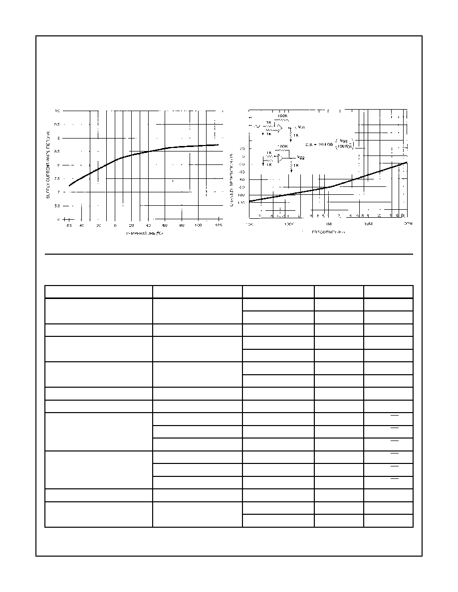
SUPPLY CURRENT/AMPLIFIER vs TEMPERATURE
CHANNEL SEPARATION vs FREQUENCY
TYPICAL PERFORMANCE CHARACTERISTICS
Device Characterized at: Supply Voltage =
±
15V, R
L
= 1k
, C
L
= 50pF, Unless Otherwise Specified
PARAMETERS
CONDITIONS
TEMPERATURE
TYPICAL
UNITS
Input Offset Voltage
See Table 1
+25
o
C
0.30
mV
Full
0.35
mV
Average Offset Voltage Drift
See Table 1
Full
0.50
µ
V/
o
C
Input Bias Current
See Table 1
+25
o
C
40
nA
Full
70
nA
Input Offset Current
See Table 1
+25
o
C
15
nA
Full
30
nA
Differential Input Resistance
See Table 1
+25
o
C
70
k
Input Noise Voltage
f
O
= 0.1Hz to 10Hz
+25
o
C
0.33
µ
V
P-P
Input Noise Voltage Density
f
O
= 10Hz
+25
o
C
6.4
nV/
Hz
f
O
= 100Hz
+25
o
C
3.7
nV/
Hz
f
O
= 1kHz
+25
o
C
3.3
nV/
Hz
Input Noise Current Density
f
O
= 10Hz
+25
o
C
8
pA/
Hz
f
O
= 100Hz
+25
o
C
2.7
pA/
Hz
f
O
= 1kHz
+25
o
C
1.3
pA/
Hz
THD & N
See Note 1
+25oC
0.005
%
Large Signal Voltage Gain
V
OUT
= 0V to
±
10V
+25oC
128
dB
Full
120
dB
Spec Number
511062-883
DESIGN INFORMATION
(Continued)
The information contained in this section has been developed through characterization by Harris Semiconductor and is for use as application
and design information only. No guarantee is implied.
3-175
HA-5222
Common Mode Rejection Ratio
V
CM
=
±
10V
Full
95
dB
Unity Gain Bandwidth
-3dB
+25
o
C
40
MHz
+125
o
C
33
MHz
-55
o
C
50
MHz
Gain Bandwidth Product
1kHz to 400kHz
+25
o
C
140
MHz
+125
o
C
115
MHz
-55
o
C
160
MHz
Minimum Gain Stability
Full
1
V/V
Output Voltage Swing
R
L
= 333
Full
110
V
R
L
= 1K
+25
o
C
112.5
V
Full
112.1
V
Output Current
V
OUT
=
±
10V
Full
156
mA
Output Resistance
+25
o
C
10
V
Full Power Bandwidth
FPBW = SR/2
V
PEAK
,
V
PEAK
= 10V
+25
o
C
398
kHz
Channel Separation
f
O
= 10kHz
+25
o
C
110
dB
Slew Rate
V
OUT
=
±
2.5V
+25
o
C
37
V/
µ
s
+125
o
C
39
V/
µ
s
-55
o
C
36
V/
µ
s
Rise Time
V
OUT
=
±
100mV
+25
o
C
16
ns
+125
o
C
17
ns
-55
o
C
17
ns
Overshoot
V
OUT
=
±
100mV
+25
o
C
12
%
+125
o
C
11
%
-55
o
C
12
%
Settling Time
10V
STEP
, A
V
= -1
0.1%
+25
o
C
0.4
µ
s
0.01%
+25
o
C
1.5
µ
s
Power Supply Rejection Ratio
V
S
=
±
10V to
±
20V
Full
100
dB
Supply Current
Quiescent, V
OUT
= 0V,
I
OUT
= 0mA
Full
8
mA/Op Amp
Minimum Supply Voltage
Functional Operation Only.
Other Parameters May Vary.
+25
o
C
15
V
NOTE:
1. A
VCL
= 10, f
O
= 1kHz, V
OUT
= 5Vrms, R
L
= 600
, 10Hz to 100kHz, Minimum resolution of test equipment is 0.005%.
TYPICAL PERFORMANCE CHARACTERISTICS (Continued)
Device Characterized at: Supply Voltage =
±
15V, R
L
= 1k
, C
L
= 50pF, Unless Otherwise Specified
PARAMETERS
CONDITIONS
TEMPERATURE
TYPICAL
UNITS
Spec Number
511062-883
3-176
All Intersil semiconductor products are manufactured, assembled and tested under ISO9000 quality systems certification.
Intersil products are sold by description only. Intersil Corporation reserves the right to make changes in circuit design and/or specifications at any time without
notice. Accordingly, the reader is cautioned to verify that data sheets are current before placing orders. Information furnished by Intersil is believed to be accurate
and reliable. However, no responsibility is assumed by Intersil or its subsidiaries for its use; nor for any infringements of patents or other rights of third parties which
may result from its use. No license is granted by implication or otherwise under any patent or patent rights of Intersil or its subsidiaries.
For information regarding Intersil Corporation and its products, see web site http://www.intersil.com
Sales Office Headquarters
NORTH AMERICA
Intersil Corporation
P. O. Box 883, Mail Stop 53-204
Melbourne, FL 32902
TEL: (321) 724-7000
FAX: (321) 724-7240
EUROPE
Intersil SA
Mercure Center
100, Rue de la Fusee
1130 Brussels, Belgium
TEL: (32) 2.724.2111
FAX: (32) 2.724.22.05
ASIA
Intersil (Taiwan) Ltd.
Taiwan Limited
7F-6, No. 101 Fu Hsing North Road
Taipei, Taiwan
Republic of China
TEL: (886) 2 2716 9310
FAX: (886) 2 2715 3029
HA-5222
Spec Number
511062-883