1
June 1998
HA-5137/883
60MHz, Ultra Low Noise, Precision
Operational Amplifier
Features
∑ This Circuit is Processed in Accordance to MIL-STD-
883 and is Fully Conformant Under the Provisions of
Paragraph 1.2.1.
∑ High Slew Rate . . . . . . . . . . . . . . . . . . . . . . 14V/
µ
s (Min)
∑ Wide Gain Bandwidth (A
V
5) . . . . . . . . . 60MHz (Min)
∑ Low Noise (at 1kHz) . . . . . . . . . . . . . . . 4.5nV/
Hz (Max)
∑ Low Offset Voltage. . . . . . . . . . . . . . . . . . . .100
µ
V (Max)
∑ Low Offset Drift With Temperature. . . . 1.8
µ
V/
o
C (Max)
∑ High CMRR . . . . . . . . . . . . . . . . . . . . . . . . . . 100dB (Min)
∑ High Voltage Gain . . . . . . . . . . . . . . . . . . 700kV/V (Min)
Applications
∑ High Speed Signal Conditioners
∑ Wide Bandwidth Instrumentation Amplifiers
∑ Low Level Transducer Amplifiers
∑ Fast, Low Level Voltage Comparators
∑ Highest Quality Audio Preamplifiers
∑ Pulse/RF Amplifiers
Description
The HA-5137/883 monolithic operational amplifier features
an excellent combination of precision DC and wideband high
speed characteristics. Utilizing the Intersil DI technology and
advanced processing techniques, this unique design unites
low noise precision instrumentation performance with high
speed, wideband capability.
This amplifier's impressive list of features include low V
OS
,
wide gain-bandwidth, high open loop gain, and high CMRR.
Additionally, this flexible device operates over a wide supply
range while consuming only 120mW of power.
Using the HA-5137/883 allows designers to minimize errors
while maximizing speed and bandwidth in applications
requiring gains greater than five.
This device is ideally suited for low level transducer signal
amplifier circuits. Other applications which can utilize the
HA-5137/883's qualities include instrumentation amplifiers,
pulse or RF amplifiers, audio preamplifiers, and signal
conditioning circuits.
Ordering Information
PART NUMBER
TEMP.
RANGE (
o
C)
PACKAGE
PKG.
NO.
HA2-5137/883
-55 to 125
8 Pin Metal Can
T8.C
HA4-5137/883
-55 to 125
20 Ld CLCC
J20.A
HA7-5137/883
-55 to 125
8 Ld CERDIP
F8.3A
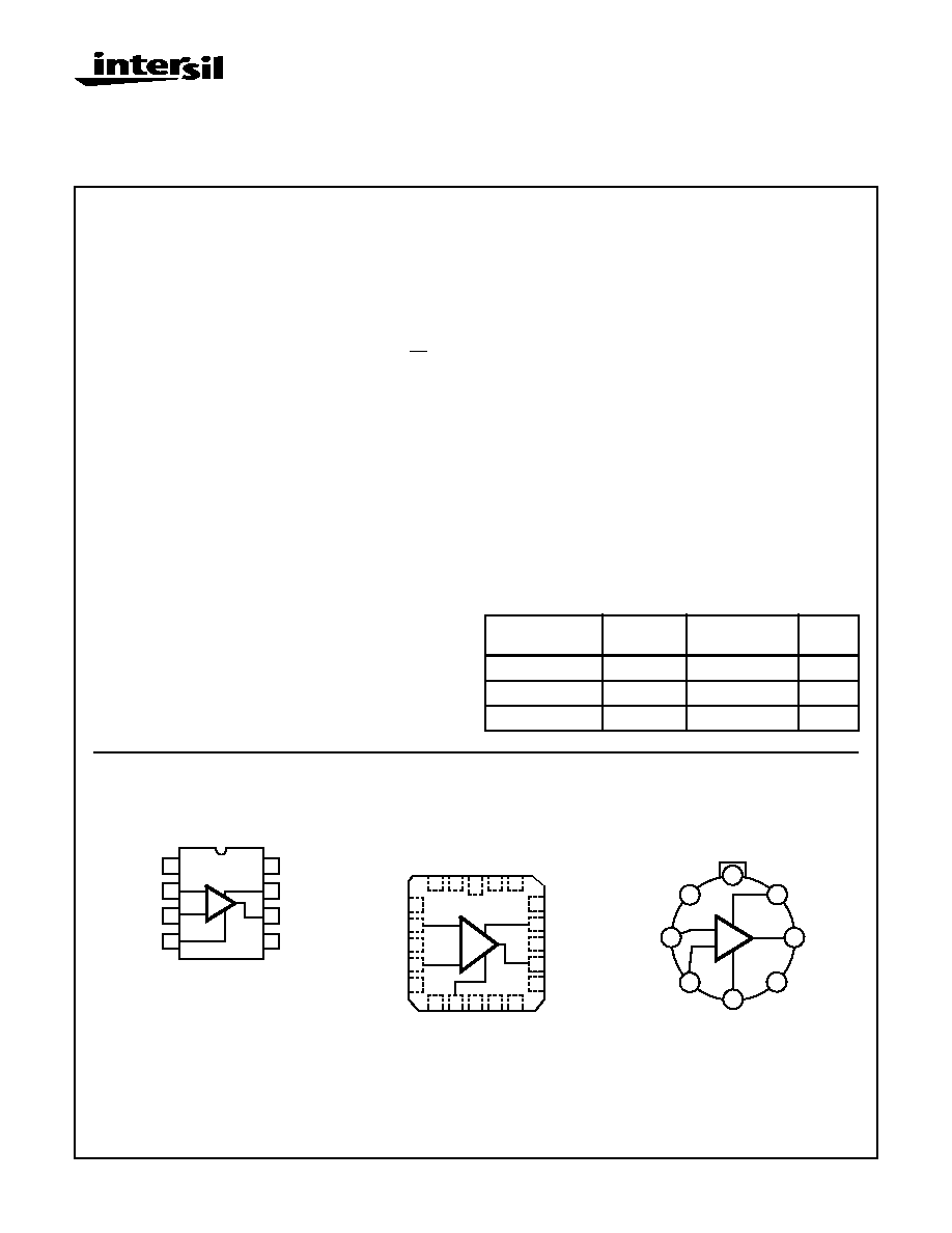
Pinouts
HA-5137/883
(CERDIP)
TOP VIEW
HA-5137/883
(CLCC)
TOP VIEW
HA-5137/883
(METAL CAN)
TOP VIEW
1
2
3
4
8
7
6
5
V+
OUT
BAL
V-
+
BAL
NC
-IN
+IN
-
4
5
6
7
8
9
10 11 12 13
3
2
1
20 19
15
14
18
17
16
BA
L
NC
V-
NC
NC
NC
NC
NC
V+
OUT
NC
NC
NC
NC
BA
L
NC
NC
+
NC
-IN
+IN
-
2
4
6
1
3
7
5
8
OUT
V- (CASE)
BAL
V+
+
BAL
-IN
+IN
NC
-
Spec Number
511034-883
File Number
3714.1
CAUTION: These devices are sensitive to electrostatic discharge; follow proper IC Handling Procedures.
1-888-INTERSIL or 321-724-7143
|
Copyright
©
Intersil Corporation 1999
2
Spec Number
511034-883
Absolute Maximum Ratings
Thermal Information
Voltage Between V+ and V- Terminals . . . . . . . . . . . . . . . . . . . . 44V
Differential Input Voltage (Note 1). . . . . . . . . . . . . . . . . . . . . . . . 0.7V
Voltage at Either Input Terminal . . . . . . . . . . . . . . . . . . . . . . V+ to V-
Input Current. . . . . . . . . . . . . . . . . . . . . . . . . . . . . . . . . . . . . . . 25mA
Output Current . . . . . . . . . . . . . . . . . . . Full Short Circuit Protection
ESD Rating. . . . . . . . . . . . . . . . . . . . . . . . . . . . . . . . . . . . . . <2000V
Operating Conditions
Temperature Range . . . . . . . . . . . . . . . . . . . . . . . . . -55
o
C to 125
o
C
Supply Voltage Range . . . . . . . . . . . . . . . . . . . . . . . . . . . . . . .
±
15V
V
INCM
1/2 (V+ - V-)
R
L
600
Thermal Resistance (Typical, Note 2)
JA
(
o
C/W)
JC
(
o
C/W)
CERDIP Package . . . . . . . . . . . . . . . .
115
28
CLCC Package . . . . . . . . . . . . . . . . . .
85
26
Metal Can Package . . . . . . . . . . . . . . .
155
67
Package Power Dissipation Limit at 75
o
C for T
J
175
o
C
CERDIP Package . . . . . . . . . . . . . . . . . . . . . . . . . . . . . . . 870mW
CLCC Package . . . . . . . . . . . . . . . . . . . . . . . . . . . . . . . . . . 1.18W
Metal Can Package . . . . . . . . . . . . . . . . . . . . . . . . . . . . . . 645mW
Package Power Dissipation Derating Factor Above 75
o
C
CERDIP Package . . . . . . . . . . . . . . . . . . . . . . . . . . . . . 8.7mW/
o
C
CLCC Package . . . . . . . . . . . . . . . . . . . . . . . . . . . . . . 11.8mW/
o
C
Metal Can Package . . . . . . . . . . . . . . . . . . . . . . . . . . . . 6.5mW/
o
C
Maximum Junction Temperature (T
J
) . . . . . . . . . . . . . . . . . . . 175
o
C
Maximum Storage Temperature Range . . . . . . . . . . -65
o
C to150
o
C
Maximum Lead Temperature (Soldering 10s) . . . . . . . . . . . . . 300
o
C
CAUTION: Stresses above those listed in "Absolute Maximum Ratings" may cause permanent damage to the device. This is a stress only rating and operation
of the device at these or any other conditions above those indicated in the operational sections of this specification is not implied.
NOTES:
1. For differential input voltages greater than 0.7V, the input current must be limited to 25mA to protect the back-to-back input diodes.
2.
JA
is measured with the component mounted on an evaluation PC board in free air.
TABLE 1. DC ELECTRICAL PERFORMANCE SPECIFICATIONS
Device Tested at: V
SUPPLY
=
±
15V, R
SOURCE
= 5
0
, R
LOAD
= 100k
, V
OUT
= 0V, Unless Otherwise Specified.
PARAMETER
SYMBOL
CONDITIONS
GROUP A
SUBGROUPS
TEMP. (
o
C)
MIN
MAX
UNITS
Input Offset Voltage
V
IO
V
CM
= 0V
1
25
-100
100
µ
V
2, 3
125, -55
-300
300
µ
V
Input Bias Current
I
B
V
CM
= 0V,
R
S
= 10k
, 5
0
1
25
-
80
nA
2, 3
125, -55
-
150
nA
Input Offset Current
I
IO
V
CM
= 0V,
+R
S
= 10k
,
-R
S
= 10k
1
25
-75
75
nA
2, 3
125, -55
-135
135
nA
Common Mode
Range
+CMR
V+ = +4.7V,
V- = -25.3V
1
25
10.3
-
V
2, 3
125, -55
10.3
-
V
-CMR
V+ = 25.3V,
V- = -4.7V
1
25
-
-10.3
V
2, 3
125, -55
-
-10.3
V
Large Signal Voltage
Gain
+A
VOL
V
OUT
= 0V and +10V,
R
L
= 2k
4
25
700
-
kV/V
5, 6
125, -55
300
-
kV/V
-A
VOL
V
OUT
= 0V and -10V,
R
L
= 2k
4
25
700
-
kV/V
5, 6
125, -55
300
-
kV/V
Common Mode
Rejection Ratio
+CMRR
V
CM
= +11V
1
25
100
-
dB
V
CM
= +10V
2, 3
125, -55
100
-
dB
-CMRR
V
CM
= -11V
1
25
100
-
dB
V
CM
= -10V
2, 3
125, -55
100
-
dB
+I
B
+ -I
B
2
---------------------------
HA-5137/883
3
Output Voltage Swing
+V
OUT1
R
L
= 2k
4
25
11.5
-
V
5, 6
125, -55
11.5
-
V
-V
OUT1
R
L
= 2k
4
25
-
-11.5
V
5, 6
125, -55
-
-11.5
V
+V
OUT2
R
L
= 600
4
25
10
-
V
-V
OUT2
R
L
= 600
4
25
-
-10
V
Output Current
+I
OUT
V
OUT
= -10V
4
25
16.5
-
mA
-I
OUT
V
OUT
= +10V
4
25
-
-16.5
mA
Quiescent Power
Supply Current
+I
CC
V
OUT
= 0V, I
OUT
= 0mA
1
25
-
4
mA
2, 3
125, -55
-
4
mA
-I
CC
V
OUT
= 0V, I
OUT
= 0mA
1
25
-4
-
mA
2, 3
125, -55
-4
-
mA
Power Supply
Rejection Ratio
+PSRR
V
SUP
= 14V,
V+ = +4V, V- = -15V,
V+ = +18V, V- = -15V
1
25
86
-
dB
2, 3
125, -55
86
-
dB
-PSRR
V
SUP
= 14V,
V+ = +15V, V- = -4V,
V+ = +15V, V- = -18V
1
25
86
-
dB
2, 3
125, -55
86
-
dB
Offset Voltage
Adjustment
+V
IO
Adj
Note 3
1
25
V
IO
-1
-
mV
2, 3
125, -55
V
IO
-1
-
mV
-V
IO
Adj
Note 3
1
25
V
IO
+1
-
mV
2, 3
125, -55
V
IO
+1
-
mV
NOTE:
3. Offset adjustment range is [V
IO
(Measured)
±
1mV] minimum referred to output. This test is for functionality only to assure adjustment
through 0V.
TABLE 1. DC ELECTRICAL PERFORMANCE SPECIFICATIONS (Continued)
Device Tested at: V
SUPPLY
=
±
15V, R
SOURCE
= 5
0
, R
LOAD
= 100k
, V
OUT
= 0V, Unless Otherwise Specified.
PARAMETER
SYMBOL
CONDITIONS
GROUP A
SUBGROUPS
TEMP. (
o
C)
MIN
MAX
UNITS
TABLE 2. AC ELECTRICAL PERFORMANCE SPECIFICATIONS
Device Tested at: V
SUPPLY
=
±
15V, R
SOURCE
= 50
, R
LOAD
= 2k
, C
LOAD
= 50pF, A
VCL
= +10V/V, Unless Otherwise Specified.
PARAMETER
SYMBOL
CONDITIONS
GROUP A
SUBGROUPS
TEMP. (
o
C)
MIN
MAX
UNITS
Slew Rate
+SR
V
OUT
= -3V to +3V
7
25
14
-
V/
µ
s
-SR
V
OUT
= +3V to -3V
7
25
14
-
V/
µ
s
Rise and Fall Time
t
r
V
OUT
= 0 to +200mV
10%
t
r
90%
7
25
-
100
ns
t
f
V
OUT
= 0 to -200mV
10%
t
f
90%
7
25
-
100
ns
Overshoot
+OS
V
OUT
= 0 to +200mV
7
25
-
40
%
-OS
V
OUT
= 0 to -200mV
7
25
-
40
%
HA-5137/883
Spec Number
511034-883
4
Spec Number
511034-883
TABLE 3. ELECTRICAL PERFORMANCE SPECIFICATIONS
Device Characterized at: V
SUPPLY
=
±
15V, R
LOAD
= 2k
, C
LOAD
= 50pF, A
V
= +5V/V, Unless Otherwise Specified.
PARAMETER
SYMBOL
CONDITIONS
NOTES
TEMP. (
o
C)
MIN
MAX
UNITS
Average Offset Voltage
Drift
V
IO
TC
V
CM
= 0V
4
-55 to 125
-
1.8
µ
V/
o
C
Differential Input
Resistance
R
IN
V
CM
= 0V
4
25
0.8
-
M
Low Frequency
Peak-to-Peak Noise
E
NP-P
0.1Hz to 10Hz
4
25
-
0.25
µ
V
P-P
Input Noise Voltage
Density
E
N
R
S
= 20
, f
O
= 10Hz
4
25
-
10
nV
/
Hz
R
S
= 20
, f
O
= 100Hz
4
25
-
5.6
nV
/
Hz
R
S
= 20
, f
O
= 1kHz
4
25
-
4.5
nV
/
Hz
Input Noise Current
Density
I
N
R
S
= 2M
, f
O
= 10Hz
4
25
-
4.0
pA
/
Hz
R
S
= 2M
, f
O
= 100Hz
4
25
-
2.3
pA
/
Hz
R
S
= 2M
, f
O
= 1kHz
4
25
-
0.6
pA
/
Hz
Gain Bandwidth Product
GBWP
V
O
= 100mV, f
O
=
10kHz
4
25
60
-
MHz
V
O
= 100mV, f
O
=
1MHz
4
25
43
-
MHz
Full Power Bandwidth
FPBW
V
PEAK
= 10V
4, 5
25
220
-
kHz
Minimum Closed Loop
Stable Gain
CLSG
R
L
= 2k
, C
L
= 50pF
4
-55 to 125
±
5
-
V/V
Settling Time
t
S
To 0.1% for a 10V Step
4
25
-
1.5
µ
s
Output Resistance
R
OUT
Open Loop
4
25
-
100
Quiescent Power
Consumption
PC
V
OUT
= 0V, I
OUT
= 0mA
4, 6
-55 to 125
-
120
mW
NOTES:
4. Parameters listed in Table 3 are controlled via design or process parameters and are not directly tested at final production. These param-
eters are lab characterized upon initial design release, or upon design changes. These parameters are guaranteed by characterization
based upon data from multiple production runs which reflect lot to lot and within lot variation.
5. Full Power Bandwidth guarantee based on Slew Rate measurement using FPBW = Slew Rate/(2
V
PEAK
).
6. Quiescent Power Consumption based upon Quiescent Supply Current test maximum. (No load on output.)
TABLE 4. ELECTRICAL TEST REQUIREMENTS
MIL-STD-883 TEST REQUIREMENTS
SUBGROUPS (SEE TABLES 1 AND 2)
Interim Electrical Parameters (Pre Burn-In)
1
Final Electrical Test Parameters
1 (Note 7), 2, 3, 4, 5, 6, 7
Group A Test Requirements
1, 2, 3, 4, 5, 6, 7
Groups C and D Endpoints
1
NOTE:
7. PDA applies to Subgroup 1 only.
HA-5137/883
5
Die Characteristics
DIE DIMENSIONS:
104.3 x 65 x 19 mils
2650 x 1650 x 483
µ
m
METALLIZATION:
Type: Al, 1% Cu
Thickness: 16k
≈
±
2k
≈
GLASSIVATION:
Type: Nitride (Si
3
N
4
) over Silox (SiO
2
, 5% Phos.)
Silox Thickness: 12k≈
±
2k≈
Nitride Thickness: 3.5k≈
±
1.5k≈
WORST CASE CURRENT DENSITY:
3.6 x 10
5
A/cm
2
at 15mA
This device meets Glassivation Integrity Test Requirement
per MIL-STD-883 Method 2021 and MIL-I-38535 Paragraph
30.5.5.4.
SUBSTRATE POTENTIAL (Powered Up):
V-
TRANSISTOR COUNT:
63
PROCESS:
Bipolar Dielectric Isolation
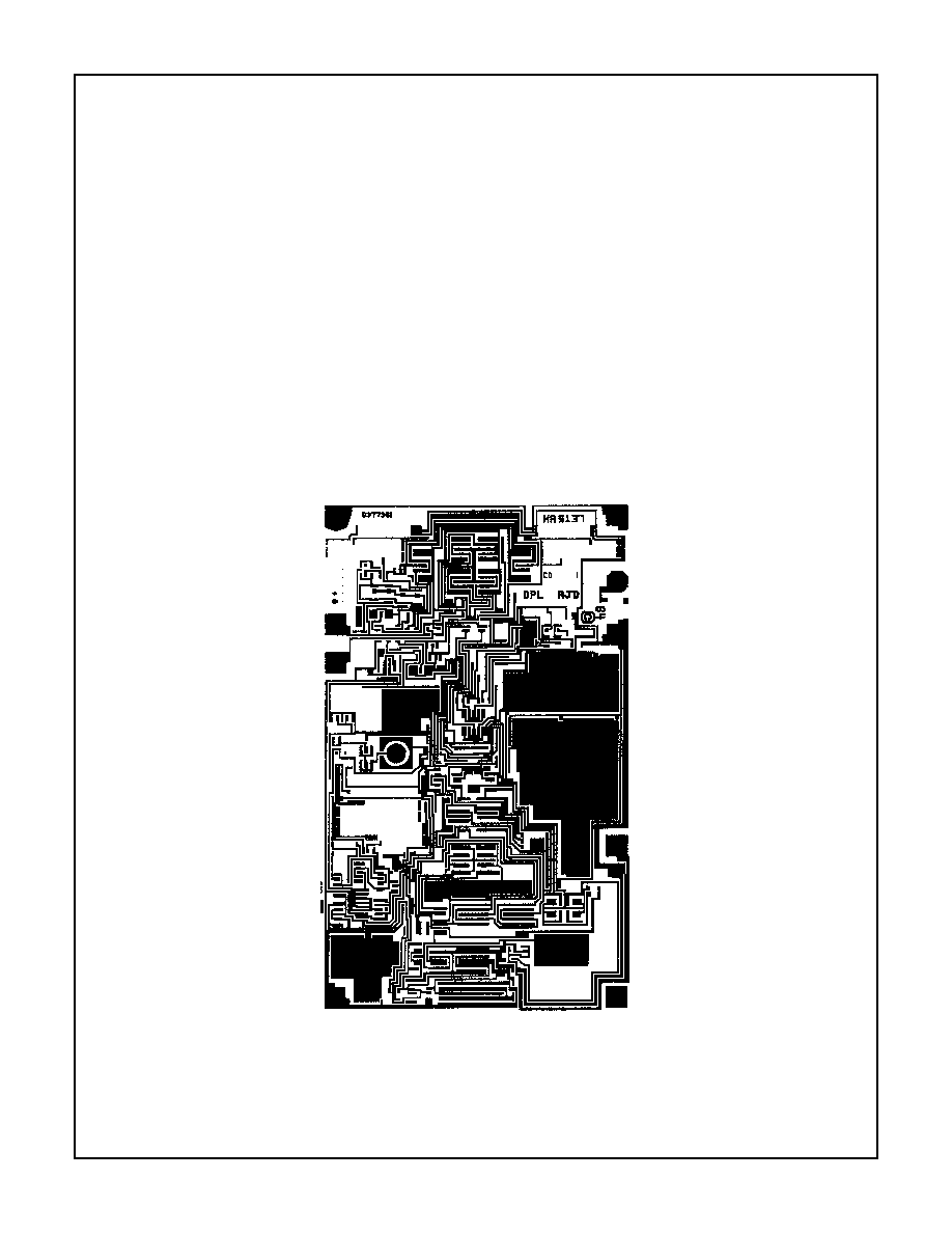
Metallization Mask Layout
HA-5137/883
BAL
BAL
V+
OUT
NC
V-
+IN
-IN
HA-5137/883
Spec Number
511034-883
6
Spec Number
511034-883
HA-5137/883
Metal Can Packages (Can)
NOTES:
1. (All leads) ÿb applies between L1 and L2. ÿb1 applies between
L2 and 0.500 from the reference plane. Diameter is uncontrolled
in L1 and beyond 0.500 from the reference plane.
2. Measured from maximum diameter of the product.
3.
is the basic spacing from the centerline of the tab to terminal 1
and
is the basic spacing of each lead or lead position (N -1
places) from
,
looking at the bottom of the package.
4. N is the maximum number of terminal positions.
5. Dimensioning and tolerancing per ANSI Y14.5M - 1982.
6. Controlling dimension: INCH.
ÿb
ÿD2
ÿ
e
k1
k
ÿb1
BASE AND
SEATING PLANE
F
Q
ÿD ÿD1
L1
L2
REFERENCE PLANE
L
A
ÿb2
ÿb1
BASE METAL
LEAD FINISH
SECTION A-A
A
A
N
e
1
C
L
2
1
T8.C
MIL-STD-1835 MACY1-X8 (A1)
8 LEAD METAL CAN PACKAGE
SYMBOL
INCHES
MILLIMETERS
NOTES
MIN
MAX
MIN
MAX
A
0.165
0.185
4.19
4.70
-
ÿb
0.016
0.019
0.41
0.48
1
ÿb1
0.016
0.021
0.41
0.53
1
ÿb2
0.016
0.024
0.41
0.61
-
ÿD
0.335
0.375
8.51
9.40
-
ÿD1
0.305
0.335
7.75
8.51
-
ÿD2
0.110
0.160
2.79
4.06
-
e
0.200 BSC
5.08 BSC
-
e1
0.100 BSC
2.54 BSC
-
F
-
0.040
-
1.02
-
k
0.027
0.034
0.69
0.86
-
k1
0.027
0.045
0.69
1.14
2
L
0.500
0.750
12.70
19.05
1
L1
-
0.050
-
1.27
1
L2
0.250
-
6.35
-
1
Q
0.010
0.045
0.25
1.14
-
45
o
BSC
45
o
BSC
3
45
o
BSC
45
o
BSC
3
N
8
8
4
Rev. 0 5/18/94
7
Spec Number
511034-883
HA-5137/883
Ceramic Dual-In-Line Frit Seal Packages (CERDIP)
NOTES:
1. Index area: A notch or a pin one identification mark shall be locat-
ed adjacent to pin one and shall be located within the shaded
area shown. The manufacturer's identification shall not be used
as a pin one identification mark.
2. The maximum limits of lead dimensions b and c or M shall be
measured at the centroid of the finished lead surfaces, when
solder dip or tin plate lead finish is applied.
3. Dimensions b1 and c1 apply to lead base metal only. Dimension
M applies to lead plating and finish thickness.
4. Corner leads (1, N, N/2, and N/2+1) may be configured with a
partial lead paddle. For this configuration dimension b3 replaces
dimension b2.
5. This dimension allows for off-center lid, meniscus, and glass
overrun.
6. Dimension Q shall be measured from the seating plane to the
base plane.
7. Measure dimension S1 at all four corners.
8. N is the maximum number of terminal positions.
9. Dimensioning and tolerancing per ANSI Y14.5M - 1982.
10. Controlling dimension: INCH
bbb
C A - B
S
c
Q
L
A
SEATING
BASE
D
PLANE
PLANE
-D-
-A-
-C-
-B-
D
E
S1
b2
b
A
e
M
c1
b1
(c)
(b)
SECTION A-A
BASE
LEAD FINISH
METAL
e
A/2
A
M
S
S
ccc
C A - B
M
D
S
S
aaa
C A - B
M
D
S
S
e
A
F8.3A
MIL-STD-1835 GDIP1-T8 (D-4, CONFIGURATION A)
8 LEAD CERAMIC DUAL-IN-LINE FRIT SEAL PACKAGE
SYMBOL
INCHES
MILLIMETERS
NOTES
MIN
MAX
MIN
MAX
A
-
0.200
-
5.08
-
b
0.014
0.026
0.36
0.66
2
b1
0.014
0.023
0.36
0.58
3
b2
0.045
0.065
1.14
1.65
-
b3
0.023
0.045
0.58
1.14
4
c
0.008
0.018
0.20
0.46
2
c1
0.008
0.015
0.20
0.38
3
D
-
0.405
-
10.29
5
E
0.220
0.310
5.59
7.87
5
e
0.100 BSC
2.54 BSC
-
eA
0.300 BSC
7.62 BSC
-
eA/2
0.150 BSC
3.81 BSC
-
L
0.125
0.200
3.18
5.08
-
Q
0.015
0.060
0.38
1.52
6
S1
0.005
-
0.13
-
7
90
o
105
o
90
o
105
o
-
aaa
-
0.015
-
0.38
-
bbb
-
0.030
-
0.76
-
ccc
-
0.010
-
0.25
-
M
-
0.0015
-
0.038
2, 3
N
8
8
8
Rev. 0 4/94
8
All Intersil semiconductor products are manufactured, assembled and tested under ISO9000 quality systems certification.
Intersil products are sold by description only. Intersil Corporation reserves the right to make changes in circuit design and/or specifications at any time without notice.
Accordingly, the reader is cautioned to verify that data sheets are current before placing orders. Information furnished by Intersil is believed to be accurate and reli-
able. However, no responsibility is assumed by Intersil or its subsidiaries for its use; nor for any infringements of patents or other rights of third parties which may
result from its use. No license is granted by implication or otherwise under any patent or patent rights of Intersil or its subsidiaries.
For information regarding Intersil Corporation and its products, see web site http://www.intersil.com
Spec Number
511034-883
HA-5137/883
Ceramic Leadless Chip Carrier Packages (CLCC)
D
j
x 45
o
D3
B
h x 45
o
A
A1
E
L
L3
e
B3
L1
D2
D1
e
1
E2
E1
L2
PLANE 2
PLANE 1
E3
B2
0.010
E H
S
S
0.010
E F
S
S
-E-
0.007
E F
M
S H S
B1
-H-
-F-
J20.A
MIL-STD-1835 CQCC1-N20 (C-2)
20 PAD CERAMIC LEADLESS CHIP CARRIER PACKAGE
SYMBOL
INCHES
MILLIMETERS
NOTES
MIN
MAX
MIN
MAX
A
0.060
0.100
1.52
2.54
6, 7
A1
0.050
0.088
1.27
2.23
-
B
-
-
-
-
-
B1
0.022
0.028
0.56
0.71
2, 4
B2
0.072 REF
1.83 REF
-
B3
0.006
0.022
0.15
0.56
-
D
0.342
0.358
8.69
9.09
-
D1
0.200 BSC
5.08 BSC
-
D2
0.100 BSC
2.54 BSC
-
D3
-
0.358
-
9.09
2
E
0.342
0.358
8.69
9.09
-
E1
0.200 BSC
5.08 BSC
-
E2
0.100 BSC
2.54 BSC
-
E3
-
0.358
-
9.09
2
e
0.050 BSC
1.27 BSC
-
e1
0.015
-
0.38
-
2
h
0.040 REF
1.02 REF
5
j
0.020 REF
0.51 REF
5
L
0.045
0.055
1.14
1.40
-
L1
0.045
0.055
1.14
1.40
-
L2
0.075
0.095
1.91
2.41
-
L3
0.003
0.015
0.08
0.38
-
ND
5
5
3
NE
5
5
3
N
20
20
3
Rev. 0 5/18/94
NOTES:
1. Metallized castellations shall be connected to plane 1 terminals
and extend toward plane 2 across at least two layers of ceramic
or completely across all of the ceramic layers to make electrical
connection with the optional plane 2 terminals.
2. Unless otherwise specified, a minimum clearance of 0.015 inch
(0.38mm) shall be maintained between all metallized features
(e.g., lid, castellations, terminals, thermal pads, etc.)
3. Symbol "N" is the maximum number of terminals. Symbols "ND"
and "NE" are the number of terminals along the sides of length
"D" and "E", respectively.
4. The required plane 1 terminals and optional plane 2 terminals (if
used) shall be electrically connected.
5. The corner shape (square, notch, radius, etc.) may vary at the
manufacturer's option, from that shown on the drawing.
6. Chip carriers shall be constructed of a minimum of two ceramic
layers.
7. Dimension "A" controls the overall package thickness. The maxi-
mum "A" dimension is package height before being solder dipped.
8. Dimensioning and tolerancing per ANSI Y14.5M-1982.
9. Controlling dimension: INCH.