1
CAUTION: These devices are sensitive to electrostatic discharge; follow proper IC Handling Procedures.
1-888-INTERSIL or 321-724-7143
|
Copyright
©
Intersil Corporation 1999
HA-2841
50MHz, Fast Settling, Unity Gain Stable,
Video Operational Amplifier
The HA-2841 is a wideband, unity gain stable, operational
amplifier featuring a 50MHz unity gain bandwidth, and
excellent DC specifications. This amplifier's performance is
further enhanced through stable operation down to closed
loop gains of +1, the inclusion of offset null controls, and by
its excellent video performance.
The capabilities of the HA-2841 are ideally suited for high
speed pulse and video amplifier circuits, where high slew
rates and wide bandwidth are required. Gain flatness of
0.05dB, combined with differential gain and phase
specifications of 0.03%, and 0.03 degrees, respectively,
make the HA-2841 ideal for component and composite video
applications.
A zener/nichrome based reference circuit, coupled with
advanced laser trimming techniques, yields a supply current
with a low temperature coefficient and low lot-to-lot
variability. Tighter I
CC
control translates to more consistent
AC parameters ensuring that units from each lot perform the
same way, and easing the task of designing systems for
wide temperature ranges. Critical AC parameters, Slew Rate
and Bandwidth, each vary by less than
±
5% over the
industrial temperature range (see characteristic curves).
For military grade product, refer to the HA-2841/883 data
sheet. Intersil AnswerFAX (321 724-7800), document
number 3621.
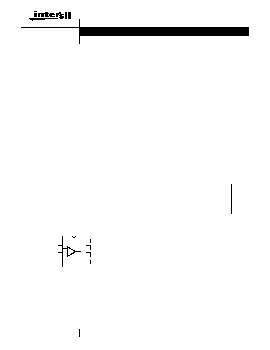
Pinout
HA-2841
(PDIP, SOIC)
TOP VIEW
Features
∑ Low Supply Current . . . . . . . . . . . . . . . . . . . . . . . . . 10mA
∑ Low AC Variability Over Process and Temperature
∑ Unity Gain Bandwidth. . . . . . . . . . . . . . . . . . . . . . . 50MHz
∑ Gain Flatness to 10MHz. . . . . . . . . . . . . . . . . . . . . 0.05dB
∑ High Slew Rate. . . . . . . . . . . . . . . . . . . . . . . . . . . 240V/
µ
s
∑ Low Offset Voltage . . . . . . . . . . . . . . . . . . . . . . . . . . . 1mV
∑ Fast Settling Time (0.1%) . . . . . . . . . . . . . . . . . . . . . . 90ns
∑ Differential Gain/Phase. . . . . . . . . . . 0.03%/0.03 Degrees
∑ Enhanced Replacement for AD841 and EL2041
Applications
∑ Pulse and Video Amplifiers
∑ Wideband Amplifiers
∑ High Speed Sample-Hold Circuits
∑ Fast, Precise D/A Converters
∑ High Speed A/D Input Buffer
BAL
-IN
+IN
V-
1
2
3
4
8
7
6
5
BAL
V+
OUT
NC
-
+
Ordering Information
PART NUMBER
(BRAND)
TEMP.
RANGE (
o
C)
PACKAGE
PKG.
NO.
HA3-2841-5
0 to 75
8 Ld PDIP
E8.3
HA9P2841-5
(H28415)
0 to 75
8 Ld SOIC
M8.15
Data Sheet
September 1998
File Number
2843.3

2
Absolute Maximum Ratings
Thermal Information
Voltage Between V+ and V- Terminals. . . . . . . . . . . . . . . . . . . . 35V
Differential Input Voltage . . . . . . . . . . . . . . . . . . . . . . . . . . . . . . . 6V
Output Current (Note 3) . . . . . . . . . . . . . . . . . . . . . . . . . . . . . . 50mA
10mA (50% Duty Cycle)
Operating Conditions
Temperature Range
HA-2841-5 . . . . . . . . . . . . . . . . . . . . . . . . . . . . . . . . 0
o
C to 75
o
C
Recommended Supply Voltage Range . . . . . . . . . . .
±
6.5V to
±
15V
Thermal Resistance (Typical, Note 2)
JA
(
o
C/W)
8 Lead PDIP Package . . . . . . . . . . . . . . . . . . . . . . .
92
8 Lead SOIC Package . . . . . . . . . . . . . . . . . . . . . . .
157
Maximum Junction Temperature (Die, Note 1) . . . . . . . . . . . . . .175
o
C
Maximum Junction Temperature (Plastic Package) . . . . . . . .150
o
C
Maximum Storage Temperature Range . . . . . . . . . . -65
o
C to 150
o
C
Maximum Lead Temperature (Soldering 10s) . . . . . . . . . . . . 300
o
C
(SOIC - Lead Tips Only)
CAUTION: Stresses above those listed in "Absolute Maximum Ratings" may cause permanent damage to the device. This is a stress only rating and operation of the
device at these or any other conditions above those indicated in the operational sections of this specification is not implied.
NOTES:
1. Maximum power dissipation, including output load, must be designed to maintain the maximum junction temperature below 150
o
C for plastic
packages.
2.
JA
is measured with the component mounted on an evaluation PC board in free air.
3. V
O
=
±
10V, R
L
unconnected. Output duty cycle must be reduced if I
OUT
>10mA.
Electrical Specifications
V
SUPPLY
=
±
15V, R
L
= 1k
, C
L
10pF, Unless Otherwise Specified
PARAMETER
TEST CONDITIONS
TEMP.
(
o
C)
HA-2841-5
UNITS
MIN
TYP
MAX
INPUT CHARACTERISTICS
Offset Voltage (Note 10)
25
-
1
3
mV
Full
-
-
6
mV
Average Offset Voltage Drift
Full
-
14
-
µ
V/
o
C
Bias Current (Note 10)
25
-
5
10
µ
A
Full
-
8
15
µ
A
Average Bias Current Drift
Full
-
45
-
nA/
o
C
Offset Current
25
-
0.5
1.0
µ
A
Full
-
-
1.5
µ
A
Input Resistance
25
-
170
-
k
Input Capacitance
25
-
1
-
pF
Common Mode Range
Full
±
10
-
-
V
Input Noise Voltage
10Hz to 1MHz
25
-
16
-
µ
V
RMS
Input Noise Voltage (Note 10)
f = 1kHz, R
SOURCE
= 0
25
-
16
-
Input Noise Current (Note 10)
f = 1kHz, R
SOURCE
= 10k
25
-
2
-
TRANSFER CHARACTERISTICS
Large Signal Voltage Gain
V
O
=
±
10V
25
25
50
-
kV/V
Full
10
30
-
kV/V
Common-Mode Rejection Ratio (Note 10)
V
CM
=
±
10V
Full
80
95
-
dB
Minimum Stable Gain
25
1
-
-
V/V
Gain Bandwidth Product (Notes 5, 10)
25
-
50
-
MHz
Gain Flatness to 5MHz (Note 10)
R
L
75
25
-
±
0.015
-
dB
Gain Flatness to 10MHz (Note 10)
R
L
500
25
-
±
0.05
-
dB
OUTPUT CHARACTERISTICS
Output Voltage Swing (Note 10)
Full
±
10
±
10.5
-
V
Output Current (Note 10)
Note 3
Full
15
30
-
mA
Output Resistance
25
-
8.5
-
Full Power Bandwidth (Note 6)
V
O
=
±
10V
25
3.2
3.8
-
MHz
Differential Gain (Note 10)
Note 4
25
-
0.03
-
%
nV
Hz
/
pA
Hz
/
HA-2841

3
Differential Phase (Note 10)
Note 4
25
-
0.03
-
Degrees
Harmonic Distortion (Note 10)
V
O
= 2V
P-P
, f = 1MHz, A
V
= +1
25
-
>83
-
dBc
TRANSIENT RESPONSE (Note 7)
Rise Time
25
-
3
-
ns
Overshoot
25
-
33
-
%
Slew Rate (Notes 9, 10)
A
V
= +1
25
200
240
-
V/
µ
s
Settling Time
10V Step to 0.1%
25
-
90
-
ns
POWER REQUIREMENTS
Supply Current (Note 10)
25
-
10
-
mA
Full
-
10
11
mA
Power Supply Rejection Ratio (Note 10)
Note 8
Full
70
80
-
dB
NOTES:
4. Differential gain and phase are measured with a VM700A video tester, using a NTC-7 composite VITS. R
F
= R
1
= 1k
, R
L
= 700
.
5. A
VCL
= 1000, Measured at unity gain crossing.
6. Full Power Bandwidth guaranteed based on slew rate measurement using
.
7. Refer to Test Circuit section of data sheet.
8. V
SUPPLY
=
±
10V to
±
20V.
9. This parameter is not tested. The limits are guaranteed based on lab characterization, and reflect lot-to-lot variation.
10. See "Typical Performance Curves" for more information.
Test Circuits and Waveforms
TEST CIRCUIT
LARGE SIGNAL RESPONSE
SMALL SIGNAL RESPONSE
Electrical Specifications
V
SUPPLY
=
±
15V, R
L
= 1k
, C
L
10pF, Unless Otherwise Specified (Continued)
PARAMETER
TEST CONDITIONS
TEMP.
(
o
C)
HA-2841-5
UNITS
MIN
TYP
MAX
FPBW
Slew Rate
2
V
PEAK
---------------------------
=
V
PEAK
10V
=
(
)
IN
OUT
+
1k
-
NOTES:
11. V
S
=
±
15V.
12. A
V
= +1.
13. C
L
< 10pF.
INPUT
OUTPUT
Input = 5V/Div.
Output = 5V/Div.
50ns/Div.
INPUT
OUTPUT
Input = 100mV/Div.
Output = 100mV/Div.
50ns/Div.
HA-2841

4
Typical Applications
(Also see Application Note AN550)
Application 1 - High Power Amplifiers and Buffers
High power amplifiers and buffers are in use in a wide variety
of applications. Many times the "high power" capability is
needed to drive large capacitive loads as well as low value
resistive loads. In both cases the final driver stage is usually a
power transistor of some type, but because of their inherently
low gain, several stages of pre-drivers are often required. The
HA-2841, with its 15mA output rating, is powerful enough to
drive a power transistor without additional stages of current
amplification. This capability is well demonstrated with the
high power buffer circuit in Figure 1.
The HA-2841 acts as the pre-driver to the output power
transistor. Together, they form a unity gain buffer with the
ability to drive three 50
coaxial cables in parallel, each with
a capacitance of 2000pF. The total combined load is 16.6
and 6000pF capacitance
.
Application 2 - Video
One of the primary uses of the HA-2841 is in the area of
video applications. These applications include signal
construction, synchronization addition and removal, as well
as signal modification. A wide bandwidth device such as the
HA-2841 is well suited for use in this class of amplifier. This,
however, is a more involved group of applications than
ordinary amplifier applications since video signals contain
precise DC levels which must be retained.
The addition of a clamping circuit restores DC levels at the
output of an amplifier stage. The circuit shown in Figure 2
utilizes the HA-5320 sample and hold amplifier as the DC
clamp. Also shown is a 3.57MHz trap in series, which will
block the color burst portion of the video signal and allow the
DC level to be amplified and restored.
Prototyping Guidelines
For best overall performance in any application, it is
recommended that high frequency layout techniques be
used. This should include:
1. Mounting the device through a ground plane.
2. Connecting unused pins (NC) to the ground plane.
3. Mounting feedback components on Teflon standoffs
and/or locating these components as close to the device
as possible.
4. Placing power supply decoupling capacitors from device
supply pins to ground.
SETTLING TIME TEST CIRCUIT
SUGGESTED OFFSET VOLTAGE ADJUSTMENT
Test Circuits and Waveforms
(Continued)
+
V-
V+
SETTLING
POINT
V
OUT
V
IN
5k
-
5k
2k
2k
NOTES:
14. A
V
= -1.
15. Load Capacitance should be less than 10pF.
16. Feedback and summing resistors must be matched to 0.1%.
17. Tektronix P6201 FET probe used at settling point.
18. HP5082-2810 clipping diodes recommended.
+
-
V-
5k
V+
OUT
BAL
D
2
HP2835
LOAD 16.6
; 6000pF
OR 12.5
; 6000pF
D
1
HP2835
+
HA-2841
-
R
3
100
50
R
1
R
2
1K
2N5886
532pF
D
3
FIGURE 1. DRIVING POWER TRANSISTORS TO GAIN
ADDITIONAL CURRENT BOOSTING
HA-2841
1k
1k
1k
1k
1k
75
3.57MHz
TRAP
HA-5320
FIGURE 2. VIDEO DC RESTORER
HA-2841

5
Typical Performance Curves
T
A
= 25
o
C, V
SUPPLY
=
±
15V, R
L
= 1k
, C
L
< 10pF, Unless Otherwise Specified
FIGURE 3. FREQUENCY RESPONSE FOR VARIOUS GAINS
FIGURE 4. GAIN BANDWIDTH PRODUCT vs SUPPLY VOLTAGE
FIGURE 5. GAIN BANDWIDTH PRODUCT vs TEMPERATURE
FIGURE 6. CMRR vs FREQUENCY
FIGURE 7. PSRR vs FREQUENCY
FIGURE 8. INPUT NOISE vs FREQUENCY
100
80
60
40
20
0
1K
10K
100K
1M
10M
100M 500M
100
FREQUENCY (Hz)
0
90
180
GAIN (dB)
PHASE (DEGREE)
OPEN
LOOP
A
VCL
= 1000
A
VCL
= 100
A
VCL
= 10
A
VCL
= 1
OPEN
LOOP
A
VCL
= 1000
A
VCL
= 100 A
VCL
= 10
A
VCL
= 1
55
45
35
GAIN B
AND
WIDTH PR
ODUCT (MHz)
6
7
8
9
10
11
12
13
14
15
SUPPLY VOLTAGE (
±
V)
30
40
50
60
65
55
40
35
-60
-40
-20
0
20
40
60
80
100
120
140
TEMPERATURE (
o
C)
GAIN B
AND
WIDTH PR
ODUCT (MHz)
30
45
50
60
100
90
80
70
60
50
40
30
CMRR (dB)
100
1K
10K
100K
1M
10M
FREQUENCY (Hz)
90
80
70
60
50
40
30
20
PSRR (dB)
100
1K
1M
10K
10M
100K
FREQUENCY (Hz)
±
PSRR
120
90
60
30
40
30
20
10
0
NOISE CURRENT (pA/
Hz)
0
NOISE V
O
L
T
A
GE (nV/
Hz)
10
100
1K
10K
100K
FREQUENCY (Hz)
NOISE CURRENT
NOISE VOLTAGE
HA-2841

6
FIGURE 9. SLEW RATE vs TEMPERATURE
FIGURE 10. SLEW RATE vs SUPPLY VOLTAGE
FIGURE 11. INPUT OFFSET VOLTAGE AND INPUT BIAS
CURRENT vs TEMPERATURE
FIGURE 12. SUPPLY CURRENT vs SUPPLY VOLTAGE
FIGURE 13. POSITIVE OUTPUT SWING vs TEMPERATURE
FIGURE 14. NEGATIVE OUTPUT SWING vs TEMPERATURE
Typical Performance Curves
T
A
= 25
o
C, V
SUPPLY
=
±
15V, R
L
= 1k
, C
L
< 10pF, Unless Otherwise Specified (Continued)
290
280
270
260
250
SLEW RA
TE (V/
µ
s)
-60
-40
-20
0
20
40
60
80
100
120
140
TEMPERATURE (
o
C)
NEGATIVE
SLEW RATE
POSITIVE
SLEW RATE
290
280
270
260
250
240
SLEW RA
TE (V/
µ
s)
7
8
9
10
11
12
13
14
15
SUPPLY VOLTAGE (
±
V)
NEGATIVE
SLEW RATE
POSITIVE
SLEW RATE
9.0
8.0
7.0
6.0
5.0
4.0
3.0
-60
-40
-20
0
20
40
60
80
100
120
140
TEMPERATURE (
o
C)
INPUT BIAS CURRENT (
µ
A)
1.5
1.0
0.5
0.0
-0.5
-1.0
-1.5
INPUT OFFSET V
O
L
T
A
GE (mV)
OFFSET
VOLTAGE
BIAS
CURRENT
12
10
8
6
4
2
5
6
7
8
9
10
11
12
13
14
15
SUPPLY VOLTAGE (
±
V)
SUPPL
Y CURRENT (mA)
125
o
C
-55
o
C
25
C
10
5
0
-60
-40
-20
0
20
40
60
80
100
120
140
TEMPERATURE (
o
C)
POSITIVE OUTPUT SWING (V)
2.5
7.5
12.5
±
15V, 150
±
15V, 1k
±
8V, 75
±
8V, 150
±
8V, 1k
±
15V, 75
-60
-40
-20
0
20
40
60
80
100
120 140
TEMPERATURE (
o
C)
NEGA
TIVE OUTPUT SWING (V)
-2.5
-7.5
-12.5
-10
-5
0
±
8V, 150
±
15V, 75
±
8V, 75
±
15V, 1k
±
15V, 150
±
8V, 1k
HA-2841

7
FIGURE 15. MAXIMUM UNDISTORTED OUTPUT SWING vs
FREQUENCY
FIGURE 16. TOTAL HARMONIC DISTORTION vs FREQUENCY
FIGURE 17. INTERMODULATION DISTORTION vs FREQUENCY
(TWO TONE)
FIGURE 18. DIFFERENTIAL GAIN vs LOAD RESISTANCE
FIGURE 19. DIFFERENTIAL PHASE vs LOAD RESISTANCE
FIGURE 20. GAIN FLATNESS vs FREQUENCY
Typical Performance Curves
T
A
= 25
o
C, V
SUPPLY
=
±
15V, R
L
= 1k
, C
L
< 10pF, Unless Otherwise Specified (Continued)
1K
10K
100K
1M
10M
100M
FREQUENCY (Hz)
25
20
15
10
5
0
OUTPUT V
O
L
T
A
GE SWING (V
P-P
)
V
SUPPLY
=
±
15V
V
SUPPLY
=
±
8V
-20
-30
-40
-50
-60
-70
-80
-90
THD (dBc)
100K
1M
10M
FREQUENCY (Hz)
V
O
= 10V
P-P
V
O
= 0.5V
P-P
V
O
= 1V
P-P
V
O
= 2V
P-P
-20
-30
-40
-50
-60
-70
-80
-90
THIRD INTERMOD PR
ODUCT (dBc)
500K
1M
10M
FREQUENCY (Hz)
V
O
= 5V
P-P
V
O
= 2V
P-P
V
O
= 1V
P-P
V
O
= 0.5V
P-P
V
O
= 0.25V
P-P
100
200
300
400
500
600
700
800
900
1000
LOAD RESISTANCE (
)
0.16
0.14
0.12
0.10
0.08
0.06
0.04
0.02
DIFFERENTIAL GAIN (%)
V
SUPPLY
=
±
8V
V
SUPPLY
=
±
10V
V
SUPPLY
=
±
15V
100
200
300
400
500 600
700
800
900
0.22
0.20
0.18
0.16
0.14
0.12
0.10
0.08
0.06
0.04
0.02
LOAD RESISTANCE (
)
DIFFERENTIAL PHASE (DEGREES)
V
SUPPLY
=
±
8V
V
SUPPLY
=
±
10V
V
SUPPLY
=
±
15V
1000
0
0.08
0.07
0.06
0.05
0.04
0.03
0.02
0.01
0.00
0
1M
2M
3M
4M
5M
6M
7M
8M
9M
10M
FREQUENCY (Hz)
GAIN FLA
TNESS (
±
dB)
A
VCL
= 1
R
L
= 75
R
L
= 150
R
L
= 500
R
L
= 1000
HA-2841

8
All Intersil semiconductor products are manufactured, assembled and tested under ISO9000 quality systems certification.
Intersil semiconductor products are sold by description only. Intersil Corporation reserves the right to make changes in circuit design and/or specifications at any time with-
out notice. Accordingly, the reader is cautioned to verify that data sheets are current before placing orders. Information furnished by Intersil is believed to be accurate and
reliable. However, no responsibility is assumed by Intersil or its subsidiaries for its use; nor for any infringements of patents or other rights of third parties which may result
from its use. No license is granted by implication or otherwise under any patent or patent rights of Intersil or its subsidiaries.
For information regarding Intersil Corporation and its products, see web site http://www.intersil.com
Die Characteristics
DIE DIMENSIONS:
77 mils x 81 mils x 19 mils
1960
µ
m x 2060
µ
m x 483
µ
m
METALLIZATION:
Type: Aluminum, 1% Copper
Thickness: 16k
≈
±
2k
≈
PASSIVATION:
Type: Nitride over Silox
Silox Thickness: 12k
≈
±
2k
≈
Nitride thickness: 3.5k
≈
±
1k
≈
SUBSTRATE POTENTIAL (Powered Up):
V-
TRANSISTOR COUNT:
43
PROCESS:
High Frequency Bipolar Dielectric Isolation
Metallization Mask Layout
HA-2841
V+
OUT
BAL
BAL
-IN
+IN
V-
HA-2841