
1
HC-5524
EIA/ITU 24V PABX SLIC with 25mA
Loop Feed
The HC-5524 telephone Subscriber Line Interface Circuit
integrates most of the BORSCHT functions on a monolithic
IC. The device is manufactured in a Dielectric Isolation (DI)
process and is designed for use as a 24V interface between
the traditional telephone subscriber pair (Tip and Ring) and
the low voltage filtering and coding/decoding functions of the
line card. Together with a secondary protection diode bridge,
the device will withstand 500V induced surges, in plastic
packages. The SLIC also maintains specified transmission
performance
in
the
presence
of
externally
induced
longitudinal currents. The BORSCHT functions that the SLIC
provides are:
∑ Battery Feed with Subscriber Loop Current Limiting
∑ Overvoltage Protection
∑ Ring Relay Driver
∑ Supervisory Signaling Functions
∑ Hybrid Functions (with External Op-Amp)
∑ Test (or Battery Reversal) Relay Driver
In addition, the SLIC provides selective denial of power to
subscriber loops, a programmable subscriber loop current
limit from 20mA to 60mA, a thermal shutdown with an alarm
output and line fault protection. Switch hook detection, ring
trip detection and ground key detection functions are also
incorporated in the SLIC device.
The HC-5524 SLIC is ideally suited for line card designs in
PBX and DLC systems, replacing traditional transformer
solutions.
Features
∑ DI Monolithic High Voltage Process
∑ Compatible with Worldwide PBX and DLC Performance
Requirements
∑ Controlled Supply of Battery Feed Current with
Programmable Current Limit
∑ Operates with 5V Positive Supply (V
B
+)
∑ Internal Ring Relay Driver and a Utility Relay Driver
∑ High Impedance Mode for Subscriber Loop
∑ High Temperature Alarm Output
∑ Low Power Consumption During Standby Functions
∑ Switch Hook, Ground Key, and Ring Trip Detection
∑ Selective Power Denial to Subscriber
∑ Voice Path Active During Power Denial
∑ On-Chip Op Amp for 2-Wire Impedance Matching
Applications
∑ Solid State Line Interface Circuit for PBX or Digital Loop
Carrier Systems
∑ Hotel/Motel Switching Systems
∑ Direct Inward Dialing (DID) Trunks
∑ Voice Messaging PBXs
∑ 2-Wire/4-Wire, 4-Wire/2-Wire Hybrid
∑ Related Literature
- AN9607, Impedance Matching Design Equations
- AN9628, AC Voltage Gain
- AN9608, Implementing Pulse Metering
- AN549, The HC-5502S/4X Telephone Subscriber Line
Interface Circuits (SLIC)
Ordering Information
PART NUMBER
TEMP.
RANGE (
o
C)
PACKAGE
PKG.
NO.
HC4P5524-9
-40 to 85
44 Ld PLCC
N44.65
HC9P5524-5
0 to 75
28 Ld SOIC
M28.3
Data Sheet
February 1999
File Number
2798.6
CAUTION: These devices are sensitive to electrostatic discharge; follow proper IC Handling Procedures.
http://www.intersil.com or 407-727-9207
|
Copyright
©
Intersil Corporation 1999
2
Absolute Maximum Ratings
(Note 1)
Thermal Information
Maximum Supply Voltages
(V
B
+) . . . . . . . . . . . . . . . . . . . . . . . . . . . . . . . . . . . . . . -0.5V to 7V
(V
B
+) - (V
B
-) . . . . . . . . . . . . . . . . . . . . . . . . . . . . . . . . . . . . . . 40V
Relay Drive Voltage . . . . . . . . . . . . . . . . . . . . . . . . . . . . -0.5V to 15V
Operating Conditions
Operating Temperature Range
HC-5524-5 . . . . . . . . . . . . . . . . . . . . . . . . . . . . 0
o
C to T
A
to 75
o
C
HC-5524-9 . . . . . . . . . . . . . . . . . . . . . . . . . . -40
o
C to T
A
to 85
o
C
Relay Driver Voltage . . . . . . . . . . . . . . . . . . . . . . . . . . . . 5V to 12V
Positive Power Supply (V
B
+) . . . . . . . . . . . . . . . . . . . . . . . . 5V
±
5%
Negative Power Supply (V
B
-). . . . . . . . . . . . . . . . . . . . -20V to -28V
Thermal Resistance (Typical, Note 2)
JA
(
o
C/W)
PLCC Package . . . . . . . . . . . . . . . . . . . . . . . . . . . . .
47
SOIC Package . . . . . . . . . . . . . . . . . . . . . . . . . . . . .
75
Maximum Junction Temperature (Plastic Package) . . . . . . . . 150
o
C
Maximum Storage Temperature Range . . . . . . -65
o
C to T
A
to 150
o
C
Maximum Lead Temperature (Soldering 10s) . . . . . . . . . . . . 300
o
C
(PLCC and SOIC - Lead Tips Only)
Die Characteristics
Transistor Count. . . . . . . . . . . . . . . . . . . . . . . . . . . . . . . . . . . . . 224
Diode Count. . . . . . . . . . . . . . . . . . . . . . . . . . . . . . . . . . . . . . . . . 28
Die Dimensions . . . . . . . . . . . . . . . . . . . . . . . . . .174 mils x 120 mils
Substrate Potential. . . . . . . . . . . . . . . . . . . . . . . . . . . . . . Connected
Process . . . . . . . . . . . . . . . . . . . . . . . . . . . . . . . . . . . . . . . Bipolar-DI
CAUTION: Stresses above those listed in "Absolute Maximum Ratings" may cause permanent damage to the device. This is a stress only rating and operation of the
device at these or any other conditions above those indicated in the operational sections of this specification is not implied.
NOTES:
1. Absolute maximum ratings are limiting values, applied individually, beyond which the serviceability of the circuit may be impaired.
Functional operability under any of these conditions is not necessarily implied.
2.
JA
is measured with the component mounted on an evaluation PC board in free air.
Electrical Specifications
Typical Parameters are at T
A
= 25
o
C, V
B
+ = 5V, V
B
- = -24V, AG = DG = BG = 0V. Min-Max Parameters are
Over Operating Positive and Negative Battery Voltages and Over the Operating Temperature Range. All
Parameters are Specified at 600W 2-Wire Terminating Impedance, Unless Otherwise Specified
PARAMETER
TEST CONDITIONS
MIN
TYP
MAX
UNITS
AC TRANSMISSION PARAMETERS
RX Input Impedance
300Hz to 3.4kHz, (Note 3)
-
100
-
k
TX Output Impedance
-
-
20
4-Wire Input Overload Level
300Hz to 3.4kHz, 600
Reference
+1.0
-
-
V
PEAK
2-Wire Return Loss
Matched for 600
,
(Note 3)
SRL LO
26
35
-
dB
ERL
30
40
-
dB
SRL HI
30
40
-
dB
2-Wire Longitudinal to Metallic Balance Off Hook
Per ANSI/IEEE STD 455-1976,
300Hz to 3400Hz, (Note 3)
58
63
-
dB
4-Wire Longitudinal Balance Off Hook
Per ANSI/IEEE STD 455-1976,
300Hz to 3400Hz, (Note 3)
50
55
-
dB
Low Frequency Longitudinal Balance
R.E.A. Test Circuit
-
-80
-67
dBmp
I
LINE
= 40mA, T
A
= 25
o
C (Note 3)
-
10
23
dBrnC
Longitudinal Current Capability
I
LINE
= 40mA, T
A
= 25
o
C (Note 3)
-
-
40
mA
RMS
Insertion Loss
2-Wire/4-Wire
-1.58dBm at 1kHz, Referenced 600
-
±
0.05
±
0.2
dB
4-Wire/2-Wire
0dBm at 1kHz, Referenced 600
-
±
0.05
±
0.2
dB
4-Wire/4-Wire
-1.58dBm at 1kHz, Referenced 600
-
-
±
0.2
dB
Frequency Response
300Hz to 3400Hz, Referenced to Absolute Level at
1kHz, 0dBm Referenced 600
(Note 3)
-
±
0.02
±
0.06
dB
Level Linearity
2-Wire to 4-Wire and 4-Wire to 2-Wire
Referenced to -10dBm, (Note 3)
+3 to -40dBm
-
-
±
0.08
dB
-40 to -50dBm
-
-
±
0.12
dB
-50 to -55dBm
-
-
±
0.3
dB
HC-5524
3
Absolute Delay
(Note 2)
2-Wire/4-Wire
300Hz to 3400Hz
-
-
1
µ
s
4-Wire/2-Wire
300Hz to 3400Hz
-
-
1
µ
s
4-Wire/4-Wire
300Hz to 3400Hz
-
0.95
1.5
µ
s
Total Harmonic Distortion
2-Wire/4-Wire, 4-Wire/2-Wire, 4-Wire/4-Wire
Reference Level 0dBm at 600
,
300Hz to 3400Hz (Note 3)
-
-
-50
dB
Idle Channel Noise
2-Wire and 4-Wire
C-Message, (Note 3)
-
-
5
dBrnC
Psophometric
-
-
-85
dBmp
3kHz Flat
-
-
16
dBrn
Open Loop Voltage (V
TIP
- V
RING
)
V
B
+ = 5V, V
B
- = -24V
-
15.8
-
V
Power Supply Rejection Ratio
V
B
+ to 2-Wire
30Hz to 200Hz, R
L
= 600
,
(Note 3)
20
40
-
dB
V
B
+ to 4-Wire
20
40
-
dB
V
B
- to 2-Wire
20
40
-
dB
V
B
- to 4-Wire
20
50
-
dB
V
B
+ to 2-Wire
200Hz to 16kHz, R
L
= 600
30
40
-
dB
V
B
+ to 4-Wire
20
28
-
dB
V
B
- to 2-Wire
20
50
-
dB
V
B
- to 4-Wire
20
50
-
dB
Ring Sync Pulse Width
50
-
500
µ
s
DC PARAMETERS
Loop Current Programming
Limit Range
20
-
60
mA
Accuracy
10
-
-
%
Loop Current During Power Denial
R
L
= 200
-
±
4
±
7
mA
Fault Currents
TIP to Ground
-
30
-
mA
RING to Ground
-
120
-
mA
TIP and RING to Ground
-
150
-
mA
Switch Hook Detection Threshold
-
12
15
mA
Ground Key Detection Threshold
-
10
-
mA
Thermal ALM Output
Safe Operating Die Temperature Exceeded
140
-
160
o
C
Ring Trip Detection Threshold
V
RING
= 105V
RMS
, f
RING
= 20Hz
-
10
-
mA
Ring Trip Detection Period
-
100
150
ms
Dial Pulse Distortion
-
0.1
0.5
ms
Relay Driver Outputs
On Voltage V
OL
I
OL
(PR) = 60mA, I
OL
(RD) = 30mA
-
0.2
0.5
V
Off Leakage Current
V
OH
= 13.2V
-
±
10
±
100
µ
A
TTL/CMOS Logic Inputs (F0, F1, RS, TST, PRI)
Logic `0' V
IL
-
-
0.8
V
Logic `1' V
IH
2.0
-
5.5
V
Input Current (F0, F1, RS, TST, PRI)
0V
V
IN
5V
-
-
±
100
µ
A
Logic Outputs
Logic `0' V
OL
I
LOAD
= 800
µ
A
-
0.1
0.5
V
Logic `1' V
OH
I
LOAD
= 40
µ
A
2.7
-
-
V
Electrical Specifications
Typical Parameters are at T
A
= 25
o
C, V
B
+ = 5V, V
B
- = -24V, AG = DG = BG = 0V. Min-Max Parameters are
Over Operating Positive and Negative Battery Voltages and Over the Operating Temperature Range. All
Parameters are Specified at 600W 2-Wire Terminating Impedance, Unless Otherwise Specified (Continued)
PARAMETER
TEST CONDITIONS
MIN
TYP
MAX
UNITS
HC-5524

4
Power Dissipation On Hook
Relay Drivers Off
-
60
-
mW
I
B
+
V
B
+ = 5.25V, V
B
- = -28V, R
LOOP
=
-
-
4
mA
I
B
-
V
B
+ = 5.25V, V
B
- = -28V, R
LOOP
=
-4
-
-
mA
I
B
+
V
B
+ = 5V, V
B
- = -24V, R
LOOP
= 600
-
3
6
mA
I
B
-
V
B
+ = 5V, V
B
- = -24V, R
LOOP
= 600
-28
-24
-
mA
UNCOMMITTED OP AMP PARAMETERS
Input Offset Voltage
-
±
5
-
mV
Input Offset Current
-
±
10
-
nA
Differential Input Resistance
(Note 3)
-
1
-
M
Output Voltage Swing
R
L
= 10k
-
±
3
-
V
P-P
Small Signal GBW
(Note 3)
-
1
-
MHz
NOTE:
3. These parameters are controlled by design or process parameters and are not directly tested. These parameters are characterized upon initial
design release, upon design changes which would affect these characteristics, and at intervals to assure product quality and specification com-
pliance.
Pin Descriptions
SOIC
PLCC
SYMBOL
DESCRIPTION
1
2
AG
(Note 4)
Analog Ground - To be connected to zero potential. Serves as a reference for the transmit output and receive
input terminals.
2
3
V
B
+
Positive Voltage Source - Most Positive Supply.
3
4
C
1
Capacitor #C
1
- An external capacitor to be connected between this terminal and analog ground. Required for
proper operation of the loop current limiting function.
4
8
F1
Function Address #1 - A TTL and CMOS compatible input used with F0 function address line to externally se-
lect logic functions. The three selectable functions are mutually exclusive. See Truth Table on front page. F1
should be toggled high after power is applied.
5
9
F0
Function Address #0 - A TTL and CMOS compatible input used with F1 function address line to externally se-
lect logic functions. The three selectable functions are mutually exclusive. See Truth Table on front page.
6
10
RS
Ring Synchronization Input - A TTL - compatible clock input. The clock is arranged such that a positive pulse
(50
µ
s - 500
µ
s) occurs on the zero crossing of the ring voltage source, as it appears at the RFS terminal. For
Tip side injected systems, the RS pulse should occur on the negative going zero crossing and for Ring injected
systems, on the positive going zero crossing. This ensures that the ring delay activates and deactivates when
the instantaneous ring voltage is near zero. If synchronization is not required, the pin should be tied to +5V.
7
11
SHD
Switch Hook Detection - An active low LS TTL compatible logic output. A line supervisory output.
8
12
GKD
Ground Key Detection - An active low LS TTL compatible logic output. A line supervisory output.
9
13
TST
A TTL logic input. A low on this pin will set a latch and keep the SLIC in a power down mode until the proper
F1, F0 state is set and will keep ALM low. See Truth Table on front page.
10
17
ALM
A LS TTL compatible active low output which responds to the thermal detector circuit when a safe operating
die temperature has been exceeded. When TST is forced low by an external control signal, ALM is latched low
until the proper F1, F0 state and TST input is brought high. The ALM can be tied directly to the TST pin to
power down the part when a thermal fault is detected and then reset with F0, F1. See Truth Table on front page.
It is possible to ignore transient thermal overload conditions in the SLIC by delaying the response to the TST
pin from the ALM. Care must be exercised in attempting this as continued thermal overstress may reduce com-
ponent life.
11
18
I
LIMIT
Loop Current Limit - Voltage on this pin sets the short loop current limiting conditions using a resistive voltage
divider.
12
19
OUT1
The analog output of the spare operational amplifier.
13
20
-IN1
The inverting analog input of the spare operational amplifier.
Electrical Specifications
Typical Parameters are at T
A
= 25
o
C, V
B
+ = 5V, V
B
- = -24V, AG = DG = BG = 0V. Min-Max Parameters are
Over Operating Positive and Negative Battery Voltages and Over the Operating Temperature Range. All
Parameters are Specified at 600W 2-Wire Terminating Impedance, Unless Otherwise Specified (Continued)
PARAMETER
TEST CONDITIONS
MIN
TYP
MAX
UNITS
HC-5524
5
14
22
TIP
An analog input connected to the TIP (more positive) side of the subscriber loop through a feed resistor and
ring relay contact. Functions with the RING terminal to receive voice signals from the telephone and for loop
monitoring purposes.
15
24
RING
An analog input connected to the RING (more negative) side of the subscriber loop through a feed resistor.
Functions with the TIP terminal to receive voice signals from the telephone and for loop monitoring purposes.
16
25
RFS
Ring Feed Sense - Senses RING side of the loop for Ground Key Detection. During Ring injected ringing the
ring signal at this node is isolated from RF via the ring relay. For Tip injected ringing, the RF and RFS pins must
be shorted.
17
27
V
RX
Receive Input, 4-Wire Side - A high impedance analog input. AC signals appearing at this input drive the Tip
Feed and Ring Feed amplifiers differentially.
18
31
C
2
Capacitor #2 - An external capacitor to be connected between this terminal and ground. It prevents false ring
trip detection from occurring when longitudinal currents are induced onto the subscriber loop from power lines
and other noise sources. This capacitor should be nonpolarized.
19
32
V
TX
Transmit Output, 4-Wire Side - A low impedance analog output which represents the differential voltage across
TIP and RING. Transhybrid balancing must be performed beyond this output to completely implement two to
four wire conversion. This output is referenced to analog ground. Since the DC level of this output varies with
loop current, capacitive coupling to the next stage is necessary.
20
33
PRI
A TTL compatible input used to control PR. PRI active High = PR active low.
21
34
PR
An active low open collector output. Can be used to drive a Polarity Reversal Relay.
22
35
DG
(Note 4)
Digital Ground - To be connected to zero potential. Serves as a reference for all digital inputs and outputs on
the SLIC.
23
36
RD
Ring Relay Driver - An active low open collector output. Used to drive a relay that switches ringing signals onto
the 2-Wire line.
24
37
V
FB
(Note 5)
Feedback input to the tip feed amplifier; may be used in conjunction with transmit output signal and the spare
op-amp to accommodate 2-Wire line impedance matching. (This is not used in the typical applications circuit).
25
38
TF
2
Tip Feed - A low impedance analog output connected to the TIP terminal through a feed resistor. Functions
with the RF terminal to provide loop current, and to feed voice signals to the telephone set and to sink longitu-
dinal currents. Must be tied to TF
1
.
NA
39
TF
1
Tie directly to TF
2
in the PLCC application.
26
41
RF
1
Ring Feed - A low impedance analog output connected to the RING terminal through a feed resistor. Functions
with the TF terminal to provide loop current, feed voice signals to the telephone set, and to sink longitudinal
currents. Tie directly to RF2.
NA
42
RF
2
Tie directly to RF
1
in the PLCC application.
27
43
V
B
-
The battery voltage source. The most negative supply.
28
44
BG
(Note 4)
Battery Ground - To be connected to zero potential. All loop current and some quiescent current flows into this
ground terminal.
1, 5, 6, 7,
14, 15,
16, 21,
23, 26,
28, 29,
30, 40
NC
No internal connection.
NOTES:
4. All grounds (AG, BG, and DG) must be applied before V
B
+ or V
B
-. Failure to do so may result in premature failure of the part. If a user wishes
to run separate grounds off a line card, the AG must be applied first.
5. Although not used in the typical applications circuit, V
FB
may be used in matching complex 2-Wire impedances.
Pin Descriptions
(Continued)
SOIC
PLCC
SYMBOL
DESCRIPTION
HC-5524

6
Pinouts
HC-5524 (SOIC)
TOP VIEW
HC-5524 (PLCC)
TOP VIEW
AG
VB+
C1
F1
F0
RS
SHD
GKD
TST
ALM
ILMT
OUT 1
-IN 1
TIP
BG
RF
TF
VFB
RD
PR
VTX
C2
VRX
RFS
RING
VB-
DG
PRI
28
27
26
25
24
23
22
21
20
19
18
17
16
15
1
2
3
4
5
6
7
8
9
10
11
12
13
14
TRUTH TABLE
F1
F0
Action
0
0
Normal Loop Feed
0
1
RD Active
1
0
Power Down Latch
RESET
1
0
Power on RESET
1
1
Loop Power
Denial Active
N/C
F1
F0
N/C
N/C
N/C
RS
SHD
ALM
GKD
TST
15
14
13
12
11
10
9
8
7
17
16
31
32
33
34
35
36
37
38
39
29
30
TF1
TF2
VFB
DG
VTX
C2
N/C
N/C
RD
PR
PRI
18 19 20 21 22 23 24 25 26 27 28
ILMT
OUT 1
-IN 1
TIP
RING
RFS
VRX
N/C
N/C
N/C
N/C
1
2
3
4
5
6
40
41
42
43
44
N/C
C1
VB+
AG
BG
VB-
RF2
RF1
N/C
N/C
N/C
HC-5524
7
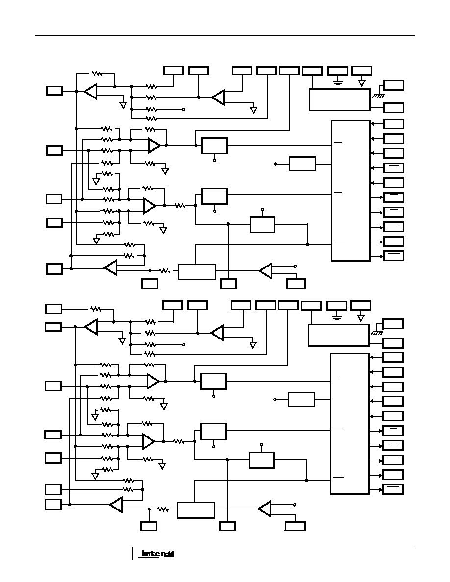
Functional Diagram
DIP OR SOIC
PLCC
R
2R
C1
R
V
RX
OUT1
2R
R/2
TIP
+
TA
R
2R
2R
R
90k
RING
RFS
LA
4.5k
25k
25k
100k
100k
4.5k
90k
RF
25
17
12
RF1
TF
14
RF
15
16
26
3
SHD
FAULT
DET
C2
I
LIMIT
OP AMP
V
FB
V
TX
RTD
GKD
GM
18
11
RF
2
BIAS
NETWORK
DG
AG
V
B
+
IIL LOGIC INTERF
A
C
E
TSD
GK
RFC
SH
F0
F1
RS
PRI
PR
ALM
GKD
SHD
RD
TST
V
B
-
REF
VB/2
-IN1
13
24
19
2
22
1
TF
BG
28
27
4
5
6
9
20
21
23
7
8
10
THERM
LTD
R = 108k
90k
-
R
R
100k
100k
90k
+
-
+
-
+
-
+
-
+
-
R
2R
C1
R
V
RX
OUT 1
2R
R/2
TIP
TA
R
2R
2R
R
90k
RING
RFS
LA
4.5k
25k
25k
100k
100k
4.5k
90k
RF
39
27
19
RF1
TF
22
RF1
24
25
41
4
SHD
FAULT
DET
C2
I
LIMIT
OP AMP
V
FB
V
TX
RTD
GKD
GM
31
18
RF
2
BIAS
NETWORK
DG
AG
V
B
+
IIL LOGIC INTERF
A
C
E
TSD
GK
RFC
SH
F0
F1
RS
PRI
PR
ALM
GKD
SHD
RD
TST
V
B
-
REF
VB/2
-IN 1
20
37
32
3
35
2
TF1
BG
44
43
8
9
10
13
33
34
36
11
12
17
THERM
LTD
90k
TF2
38
RF2
42
R
90k
100k
100k
R
+
-
+
-
+
-
+
-
+
-
+
-
NOTES:
6. R = 108k
.
7. NC = 1, 5, 6, 7, 14, 15, 16, 21,
23, 26, 28, 29, 30, 40.
HC-5524

8
Logic Diagram
Overvoltage Protection and Longitudinal Current Protection
The SLIC device, in conjunction with an external protection
bridge, will withstand high voltage lightning surges and
power line crosses.
High voltage surge conditions are as specified in Table 1.
The SLIC will withstand longitudinal currents up to a maxi-
mum or 40mA
RMS
, 20mA
RMS
per leg, without any perfor-
mance degradation.
TO BIAS
NETWORK
RD
THERMAL
SHUT DOWN
TEST
F1
SH
PD
F0
GK
RS
THERMAL
SHUTDOWN
LATCH
KEY
A
B
C
INJ
A
B
C
GKD
SHD
ALM
I
2
L TO TTL
I
2
L TO TTL
I
2
L TO TTL
RELAY
DRIVER
TTL TO I
2
L
TTL TO I
2
L
TTL TO I
2
L
TTL TO I
2
L
TABLE 1.
PARAMETER
TEST
CONDITION
PERFORMANCE
(MAX)
UNITS
Longitudinal
Surge
10
µ
s Rise/
±
1000 (Plastic)
V
PEAK
1000
µ
s Fall
Metallic Surge
10
µ
s Rise/
±
1000 (Plastic)
V
PEAK
1000
µ
s Fall
T/GND
10
µ
s Rise/
±
1000 (Plastic)
V
PEAK
R/GND
1000
µ
s Fall
50/60Hz Current
T/GND
11 Cycles
700 (Plastic)
V
RMS
R/GND
Limited to
10A
RMS
HC-5524

9
All Intersil semiconductor products are manufactured, assembled and tested under ISO9000 quality systems certification.
Intersil semiconductor products are sold by description only. Intersil Corporation reserves the right to make changes in circuit design and/or specifications at any time with-
out notice. Accordingly, the reader is cautioned to verify that data sheets are current before placing orders. Information furnished by Intersil is believed to be accurate and
reliable. However, no responsibility is assumed by Intersil or its subsidiaries for its use; nor for any infringements of patents or other rights of third parties which may result
from its use. No license is granted by implication or otherwise under any patent or patent rights of Intersil or its subsidiaries.
For information regarding Intersil Corporation and its products, see web site http://www.intersil.com
Typical Applications
Typical Component Values
C
1
= 0.5
µ
F, 20V.
C
2
= 1.0
µ
F
±
10%, 20V (for other values of C2, refer to
AN9667).
C
3
= 0.01
µ
F, 50V
±
20%.
C
4
= 0.01
µ
F, 50V
±
20%.
C
5
= 0.01
µ
F, 50V
±
20%.
C
AC
= 0.5
µ
F, 20V.
K(Z
0
- R
F
/2) = 50k
, (Z
0
= 600
, K = Scaling Factor = 100).
R
L1
, R
L2
; Current Limit Setting Resistors.
R
L1
+R
L2
> 90k
.
I
LIMIT
= (.6) (R
L1
+ R
L2
)/(200 x R
L2
), R
L1
typically 100k
.
KR
F
= 20k
, R
F
= 2(R
B1
+R
B2
), K = Scaling Factor = 100).
R
B1
= R
B2
= 50
(1% absolute, matching requirements cov-
ered in a Tech Brief).
R
S1
= R
S2
= 1k
typically.
C
S1
= C
S2
= 0.1
µ
F, 200V typically, depending on V
Ring
and
line length.
Z
1
= 150V to 200V transient protector. PTC used as ring
generator ballast.
NOTES:
8. All grounds (AG, BG, and DG) must be applied before V
B
+ or V
B
-. Failure to do so may result in premature failure of the part. If a user wishes
to run separate grounds off a line card, the AG must be applied first.
9. Application shows Ring Injected Ringing, Balanced or Tip injected configuration may be used.
10. Secondary protection diode bridge recommended is 3A, 200V type.
11. TF
1
, TF
2
and RF
1
, RF
2
are on PLCC only and should be connected together as shown.
V
B
-
BG
C
2
DG
AG
V
B
+ C
1
R
B2
C
3
C
4
5V
I
LIMIT
V
RX
+
V
FB
V
TX
-IN1
OUT1
R
L1
C
AC
FROM PCM
FILTER/CODER
SYSTEM CONTROLLER
PRI RS
F1
F0
SHD GKD
TEST
ALARM
RING
K
1A
TIP
R
S1
C
S1
PTC
Z
1
PRIMARY
PROTECTION
K
2
K
1
5V
5V
K
IB
150V
PEAK
(MAX)
V
RING
R
S2
C
S2
RF
2
(NOTE 7)
RF
1
(NOTE 7)
RFS
RING
TF
1
(NOTE 7)
TF
2
(NOTE 7)
TIP
PR
RD
R
B1
V
B
-
C
5
K
RF
R
L2
SECONDARY
PROTECTION
TO HYBRID
BALANCE
NETWORK
SLIC
HC-5524
(NOTE 6)
K(Z0 - R /2)
F
FIGURE 1. TYPICAL LINE CIRCUIT APPLICATION WITH THE MONOLITHIC SLIC
HC-5524