 | –≠–ª–µ–∫—Ç—Ä–æ–Ω–Ω—ã–π –∫–æ–º–ø–æ–Ω–µ–Ω—Ç: HC5503CCB | –°–∫–∞—á–∞—Ç—å:  PDF PDF  ZIP ZIP |
49
CAUTION: These devices are sensitive to electrostatic discharge; follow proper IC Handling Procedures.
http://www.intersil.com or 407-727-9207 | Copyright © Intersil Corporation 1999
HC5503C
Unbalanced PBX/Key System SLIC,
Subscriber Line Interface Circuit
The Intersil HC5503C is a low cost Subscriber Line Interface
Circuit (SLIC), that replaces the components of an
unbalanced discrete Analog circuit design. The monolithic
integrated design provides improved performance and
system reliability.
The SLIC provides: current limited DC feed to the subscriber
loop, maintains a flat frequency response over the voice
band and beyond, has self resetting thermal protection that
allows conversation to continue while the fault is present,
provides a TTL subscriber off-hook indication even in the
presence of longitudinal currents, provides unbalanced
2-wire transmission while maintaining an excellent
longitudinal balance and limits system power consumption
on short loops.
The HC5503C provides on-hook transmission and
longitudinal current rejection in both the on-hook or off-hook
conditions. The SLIC needs only one +5V supply in addition
to the main battery supply (-24V to -58V) for loop current.
Available in 22PDIP and 24SO packaging. The HC5503C is
ideally suited as a replacement for discrete line circuits in
low cost analog PABX's, Small Office/Home Office products
or Small Key Systems.
Features
∑ Monolithic Integrated Device
∑ Single +5V Supply
∑ Controlled Supply of Battery Feed Current for Short Loops
(30mA)
∑ Allows Interfacing With All Ringing Systems
∑ Switch Hook Detection
∑ Low Power Consumption During Standby
Applications
∑ PBX Switches (Analog, Digital or ISDN)
∑ Key Telephone Systems (KTS)
∑ ISDN PC Plug in Modems
∑ ISDN Small Office / Home Office (SOHO) Terminal Adapt-
ers (TA)
∑ CTI (Computer Telephony Integration) Products
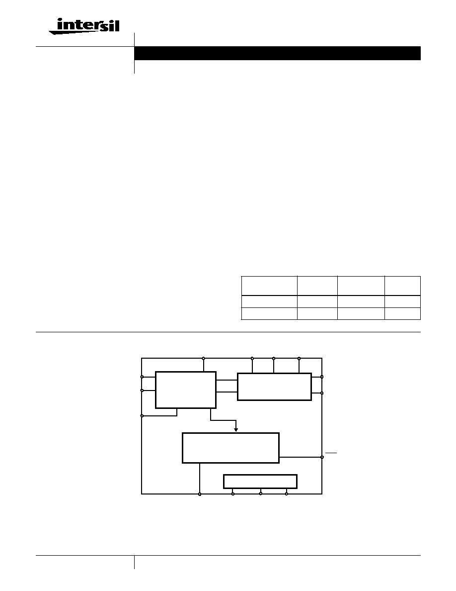
Block Diagram
Ordering Information
PART NUMBER
TEMP.
RANGE (
o
C)
PACKAGE
PKG. NO.
HC5503CCP
0 to 75
22 Ld PDIP
E22.4
HC5503CCB
0 to 75
24 Ld SOIC
M24.3
LOOP FEED
SPEECH CIRCUIT
LOOP DETECTOR
BIAS
VCC
AGND
DGND
V
BAT
VB(INT)
TF
BGND
TIP
RING
C1
TX
RX
SHD
RS
Data Sheet
June 1998
File Number
4503
50
Absolute Maximum Ratings
(Note 1)
Thermal Information
Maximum Continuous Supply Voltages
(V
BAT
). . . . . . . . . . . . . . . . . . . . . . . . . . . . . . . . . . . . . . -60 to 0.5V
(V
CC
) . . . . . . . . . . . . . . . . . . . . . . . . . . . . . . . . . . . . . . . -0.5 to 7V
(V
CC
- V
BAT
) . . . . . . . . . . . . . . . . . . . . . . . . . . . . . . . . . . . . . .75V
Operating Conditions
Temperature Range
HC5503C-5 . . . . . . . . . . . . . . . . . . . . . . . . . . . . . . . . 0
o
C to 75
o
C
Positive Supply Voltage (V
CC
) . . . . . . . . . . . . . . . . . . 4.75V to 5.25V
Negative Supply Voltage (V
BAT
) . . . . . . . . . . . . . . . . . .-24V to -58V
High Level Logic Input Voltage. . . . . . . . . . . . . . . . . . . . . . . . . . 2.4V
Low Level Logic Input Voltage . . . . . . . . . . . . . . . . . . . . . . . . . . 0.6V
Thermal Resistance (Typical, Note 2)
JA
(
o
C/W)
PDIP Package . . . . . . . . . . . . . . . . . . . . . . . . . . . . .
53
SOIC Package . . . . . . . . . . . . . . . . . . . . . . . . . . . . .
75
Maximum Junction Temperature Plastic . . . . . . . . . . . . . . . . .150
o
C
Maximum Storage Temperature Range . . . . . . . . . . -65
o
C to 150
o
C
Maximum Lead Temperature (Soldering 10s) . . . . . . . . . . . . .300
o
C
(SOIC - Lead Tips Only)
Die Characteristics
Transistor Count. . . . . . . . . . . . . . . . . . . . . . . . . . . . . . . . . . . . . . 185
Diode Count. . . . . . . . . . . . . . . . . . . . . . . . . . . . . . . . . . . . . . . . . . 36
Die Dimensions . . . . . . . . . . . . . . . . . . . . . . . . . . . . . . . . . 137 x 102
Substrate Potential. . . . . . . . . . . . . . . . . . . . . . . . . . . . . . Connected
Process . . . . . . . . . . . . . . . . . . . . . . . . . . . . . . . . . . . . . . . Bipolar-DI
CAUTION: Stresses above those listed in "Absolute Maximum Ratings" may cause permanent damage to the device. This is a stress only rating and operation of the
device at these or any other conditions above those indicated in the operational sections of this specification is not implied.
NOTES:
1. Absolute maximum ratings are limiting values, applied individually, beyond which the serviceability of the circuit may be impaired. Functional
operability under any of these conditions is not necessarily implied.
2.
JA
is measured with the component mounted on an evaluation PC board in free air.
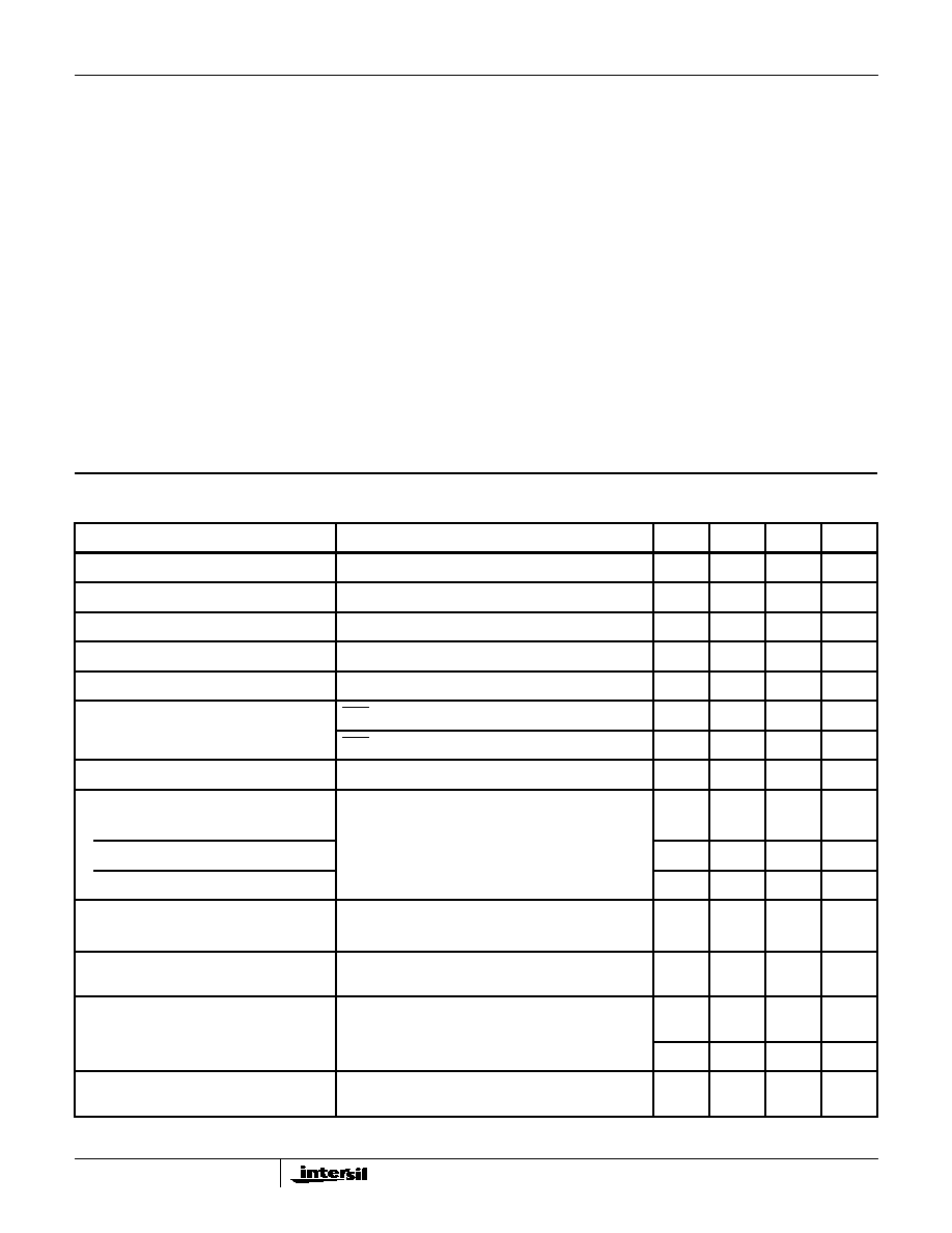
Electrical Specifications
Unless Otherwise Specified, V
BAT
= -48V, V
CC
= 5V, AG = BG = DG = 0V, Typical Parameters
T
A
= 25
o
C. Min-Max Parameters are Over Operating Temperature Range
PARAMETER
CONDITIONS
MIN
TYP
MAX
UNITS
Off-Hook I
B
+
R
L
= 600
,
T
A
= 25
o
C
-
-
5.3
mA
Off-Hook I
B
-
R
L
= 600
-
-
39
mA
Off-Hook Loop Current
R
L
= 1200
-
21
-
mA
Off-Hook Loop Current
R
L
= 1200
, V
BAT
= -42V, T
A
= 25
o
C
17.5
-
-
mA
Off-Hook Loop Current
R
L
= 200
25.5
30
34.5
mA
Switch Hook Detection Threshold
SHD = V
OL
10
-
-
mA
SHD = V
OH
-
-
5
mA
Dial Pulse Distortion
0
-
5
µ
s
Longitudinal Balance
1V
RMS
200Hz - 3400Hz, (Note 3) IEEE Method
0
o
C
T
A
75
o
C
2-Wire Off-Hook
-
65
-
dB
2-Wire On-hook
-
63
-
dB
Tip and Ring to TX, Off-hook
-
58
-
dB
Insertion Loss
At 1kHz, 0dBm Input Level, Referenced 600
-
±
0.05
±
0.2
dB
2-Wire to TX, RX to 2-Wire
Frequency Response
200 - 3400Hz Referenced to Absolute Loss at 1kHz and
0dBm Signal Level (Note 3)
-
±
0.02
±
0.05
dB
Idle Channel Noise
(Note 3)
-
1
5
dBrnC
2-Wire to TX, RX to 2-Wire
-
-89
-85
dBm0p
Trans Hybrid Loss
RX to TX
Balance Network Set Up for 600
Termination at 1kHz
-
40
-
dB
HC5503C
51
Overload Level, 2-Wire to TX, RX to 2-Wire
V
CC
= +5V, (Note 3)
2.5
-
-
V
PEAK
Level Linearity
2-Wire to TX, RX to 2-Wire
At 1kHz, (Note 3) Referenced to 0dBm Level
+3 to -40dBm
-
-
±
0.05
dB
-40 to -50dBm
-
-
±
0.1
dB
-50 to -55dBm
-
-
±
0.3
dB
Power Supply Rejection Ratio
(Note 3)
V
CC
to 2-Wire
200 - 3400kHz, R
L
= 600
-
40
-
dB
V
CC
to Transmit
-
40
-
dB
V
BAT
to 2-Wire
-
40
-
dB
V
BAT
to Transmit
-
40
-
dB
Logic Input Current ( RS)
0V
V
IN
5V
-
-
±
100
µ
A
Logic Input ( RS)
Logic `0' V
IL
-
-
0.8
V
Logic `1' V
IH
2.0
-
5.5
V
Logic Output ( SHD)
Logic `0' V
OL
I
LOAD
800
µ
A, V
CC
= 5V
-
0.1
0.5
V
Logic `1' V
OH
I
LOAD
40
µ
A, V
CC
= 5V
2.7
-
5.0
V
NOTE:
3. These parameters are controlled by design or process parameters and are not directly tested. These parameters are characterized upon initial
design release, upon design changes which would affect these characteristics, and at intervals to assure product quality and specification
compliance.
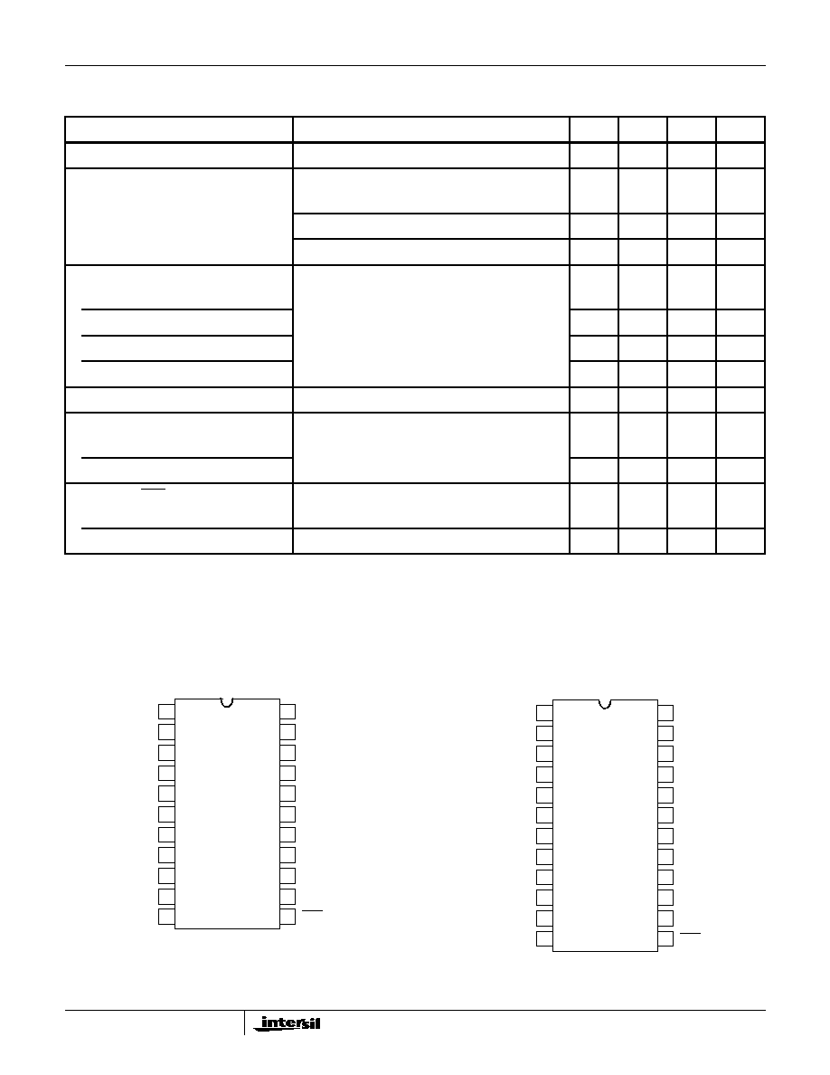
Pinouts
HC5503C (PDIP)
TOP VIEW
HC5503C (SOIC)
TOP VIEW
Electrical Specifications
Unless Otherwise Specified, V
BAT
= -48V, V
CC
= 5V, AG = BG = DG = 0V, Typical Parameters
T
A
= 25
o
C. Min-Max Parameters are Over Operating Temperature Range (Continued)
PARAMETER
CONDITIONS
MIN
TYP
MAX
UNITS
1
2
3
4
5
6
7
8
9
10
11
14
15
16
17
18
19
20
21
22
13
12
TIP
RING
DGND
RS
N/C
VB(INT)
V
BAT
TX
N/C
T3
N/C
AGND
T1
C1
RX
T2
N/C
N/C
SHD
TF
V
CC
BGND
1
2
3
4
5
6
7
8
9
10
11
12
16
17
18
19
20
21
22
23
24
15
14
13
TIP
RING
C1
DGND
RS
TF
VB(INT)
BGND
TX
N/C
T3
N/C
AGND
T1
N/C
RX
T2
N/C
N/C
N/C
SHD
N/C
V
CC
V
BAT
HC5503C

52
Pin Descriptions
PDIP
SOIC
SYMBOL
DESCRIPTION
1
1
TIP
An analog input connected to the TIP (more positive) side of the subscriber loop through a 150
feed resistor.
Functions with the Ring terminal to receive voice signals from the telephone and for loop monitoring
purposes.
2
2
RING
An analog input connected to the RING (more negative) side of the subscriber loop through a 150
feed
resistor. Functions with the Tip terminal to receive voice signals from the telephone and for loop monitoring
purposes.
3
3
V
CC
Positive Voltage Source - Most positive supply. V
CC
is typically 5V.
4
N/C
No connect. For proper operation this pin should be left floating.
4
5
C
1
Capacitor - An external capacitor to be connected between this terminal and analog ground. Required for
proper operation of the voice band hybrid. Typical value is 0.3
µ
F, 30V.
5
6
DGND
Digital Ground - To be connected to zero potential and serves as a reference for all digital inputs and outputs
on the SLIC microcircuit.
6
7
RS
This pin should be tied to 5V.
7
8
N/C
No connect. For proper operation this pin should be left floating.
8
9
TF
Tip Feed - A low impedance analog output connected to the TIP terminal through a 150
feed resistor.
Provides voice signals to the telephone set and sink longitudinal current.
9
10
VB(INT)
A low impedance analog output connected to the Ring terminal through a 150
feed resistor. This pin
provides a loop current path to battery.
10
11
V
BAT
Negative Voltage Source - Most negative supply. V
BAT
has an operational range of -24V to -58V. Frequently
referred to as "battery".
11
12
BGND
Battery Ground - To be connected to zero potential. All loop current and some quiescent current flows into
this ground terminal.
12
13
SHD
Switch Hook Detection - A low active LS TTL - compatible logic output. This output is enabled for loop
currents exceeding 10mA and disabled for loop currents less than 5mA.
13
14
N/C
No connect. For proper operation this pin should be left floating.
15
N/C
No connect. For proper operation this pin should be left floating.
14
16
N/C
No connect. For proper operation this pin should be left floating.
15
17
N/C
No connect. For proper operation this pin should be left floating.
16
18
T1
Used during production testing. For proper operation this pin should be connected to pin T2.
17
19
T2
Used during production testing. For proper operation this pin should be connected to pin T1.
18
20
T3
Used during production testing. For proper operation this pin should be connected to Analog Ground pin
AGND.
19
21
RX
Receive Input - A high impedance analog input which is internally biased. Capacitive coupling to this input is
required. AC signals appearing at this input differentially drive the Tip feed and Ring feed terminals, which in
turn drive tip and ring through 300
of feed resistance on each side of the line.
20
22
N/C
No connect. For proper operation this pin should be left floating.
21
23
AGND
Analog Ground - To be connected to zero potential and serves as a reference for the transmit output (TX)
and receive input (RX) terminals.
22
24
TX
Transmit Output - A low impedance analog output which represents the differential voltage across Tip and
Ring. This output is unbalanced and referenced to analog ground. Since the DC level of this output varies
with loop current, capacitive coupling to the next stage is essential.
NOTE: All grounds (AGND, BGND, and DGND) must be applied before V
CC
or V
BAT
. Failure to do so may result in premature failure of the part. If
a user wishes to run separate grounds off a line card, the AG must be applied first.
HC5503C
53
All Intersil semiconductor products are manufactured, assembled and tested under ISO9000 quality systems certification.
Intersil semiconductor products are sold by description only. Intersil Corporation reserves the right to make changes in circuit design and/or specifications at any time with-
out notice. Accordingly, the reader is cautioned to verify that data sheets are current before placing orders. Information furnished by Intersil is believed to be accurate and
reliable. However, no responsibility is assumed by Intersil or its subsidiaries for its use; nor for any infringements of patents or other rights of third parties which may result
from its use. No license is granted by implication or otherwise under any patent or patent rights of Intersil or its subsidiaries.
For information regarding Intersil Corporation and its products, see web site http://www.intersil.com
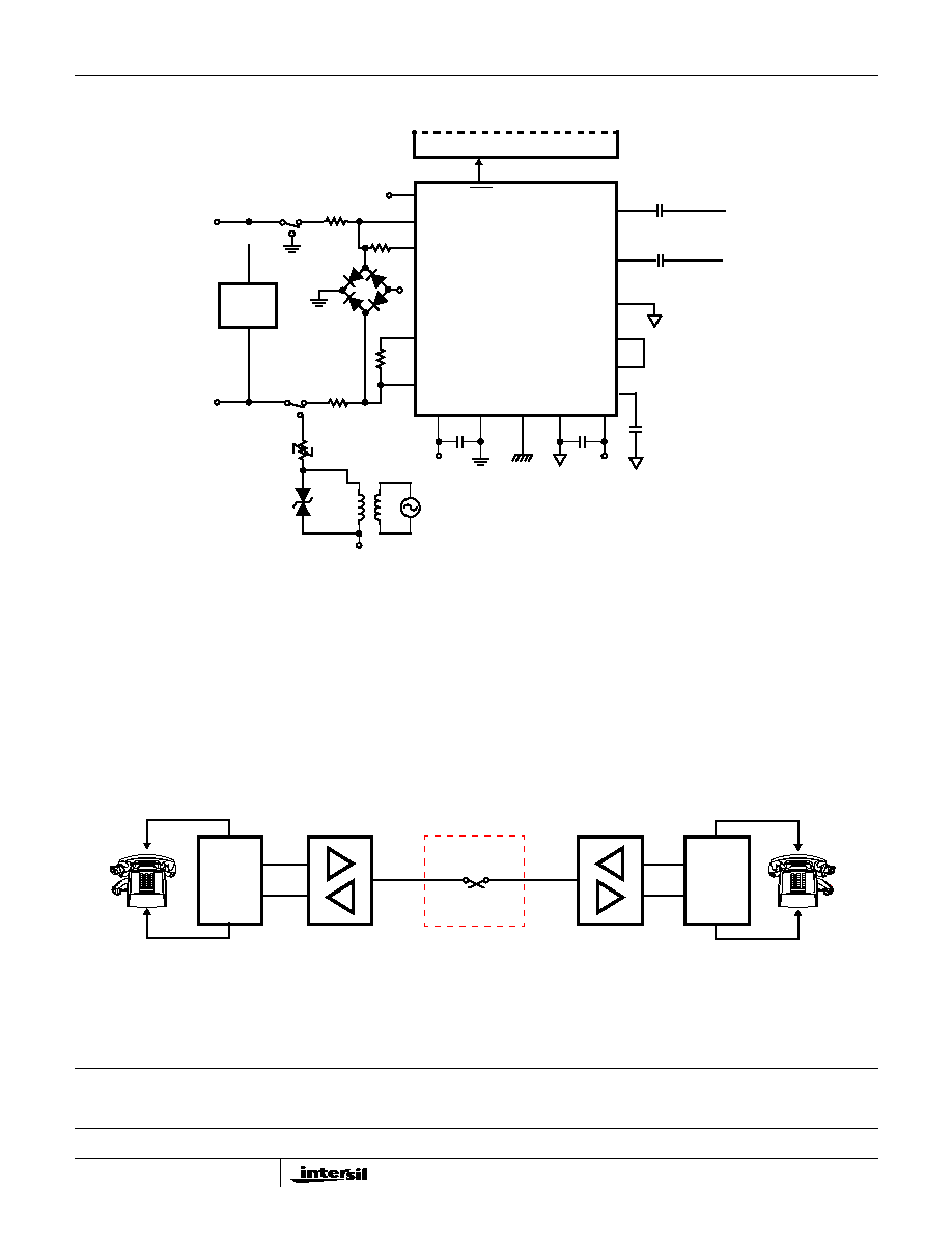
Applications Diagram
Typical Component Values
C
1
= 0.3
µ
F, 30V,
±
20%
C
2
= 0.01
µ
F, 100V,
±
20%
R
B1
= R
B2
= R
B3
= R
B4
= 150
C
3
= 0.01
µ
F, 20V,
±
20%
C
4
= 0.5
µ
F, 20V,
±
20%
C5 = 0.5
µ
F, 20V,
±
20%
PTC used as ring generator ballast.
NOTES:
4. Secondary protection diode bridge recommended is a 2A, 200V type.
5. All grounds (AG, BG, and DG) must be applied before V
CC
or V
BAT
. Failure to do so may result in premature failure of the part. If a user wishes
to run separate grounds off a line card, the AG must be applied first.
6. Application shows Ring Injected Ringing.
R
B4
K
1A
RING
VB(INT)
TIP
V
BAT
SLIC
HC5503C
R
B2
R
B1
RING
R
B3
SUBSCRIBER
LOOP
-48V
SYSTEM CONTROLLER
1
9
10
2
TIP FEED
TIP
RX
TX
T3
T2
T1
C1
V
BAT
BGND DGND AGND
V
CC
SHD
13
11
12
6
23
C
3
3
V
CC
C
2
PRIMARY
PROTEC-
TION
(NOTE 4)
PIN NUMBERS GIVEN FOR SOIC PACKAGE.
K
1A
PTC
Z
1
-48V
RING GENERATOR
RS
5V
C
1
21
24
20
19
18
5
C
4
C
5
FIGURE 1. TYPICAL LINE CIRCUIT APPLICATION WITH THE MONOLITHIC SLIC
HC5503C
SLIC
TX
RX
DUAL
JUNC
JUNC
DUAL
CD22100E
CROSSPOINT
SWITCH
TX
RX
FIGURE 2. TYPICAL ANALOG KEY SYSTEM CONNECTION
HC5503C
SLIC
HC5503C
SLIC
OP-AMP
OP-AMP
HC5503C