 | –≠–ª–µ–∫—Ç—Ä–æ–Ω–Ω—ã–π –∫–æ–º–ø–æ–Ω–µ–Ω—Ç: HC55131IM | –°–∫–∞—á–∞—Ç—å:  PDF PDF  ZIP ZIP |
4-1
TM
CAUTION: These devices are sensitive to electrostatic discharge; follow proper IC Handling Procedures.
1-888-INTERSIL or 321-724-7143
|
Intersil and Design is a trademark of Intersil Corporation.
|
Copyright
©
Intersil Corporation 2000
File Number
4659.5
HC55120, HC55121, HC55130, HC55131, HC55140,
HC55141, HC55142, HC55143, HC55150, HC55151
Low Power Universal SLIC Family
The UniSLIC14 is a family of Ultra Low Power SLICs. The
feature set and common pinouts of the UniSLIC14 family
positions it as a universal solution for: Plain Old Telephone
Service (POTS), PBX, Central Office, Loop Carrier, Fiber in the
Loop, ISDN-TA and NT1+, Pairgain and Wireless Local Loop.
The UniSLIC14 family achieves its ultra low power operation
through: Its automatic single and dual battery selection
(based on line length) and battery tracking anti clipping to
ensure the maximum loop coverage on the lowest battery
voltage. This architecture is ideal for power critical
applications such as ISDN NT1+, Pairgain and Wireless
local loop products.
The UniSLIC14 family has many user programmable
features. This family of SLICs delivers a low noise, low
component count solution for Central Office and Loop
Carrier universal voice grade designs. The product family
integrates advanced pulse metering, test and signaling
capabilities, and zero crossing ring control.
The UniSLIC14 family is designed in the Intersil "Latch" free
Bonded Wafer process. This process dielectrically isolates
the active circuitry to eliminate any leakage paths as found in
our competition's JI process. This makes the UniSLIC14
family compliant with "hot plug" requirements and operation
in harsh outdoor environments.
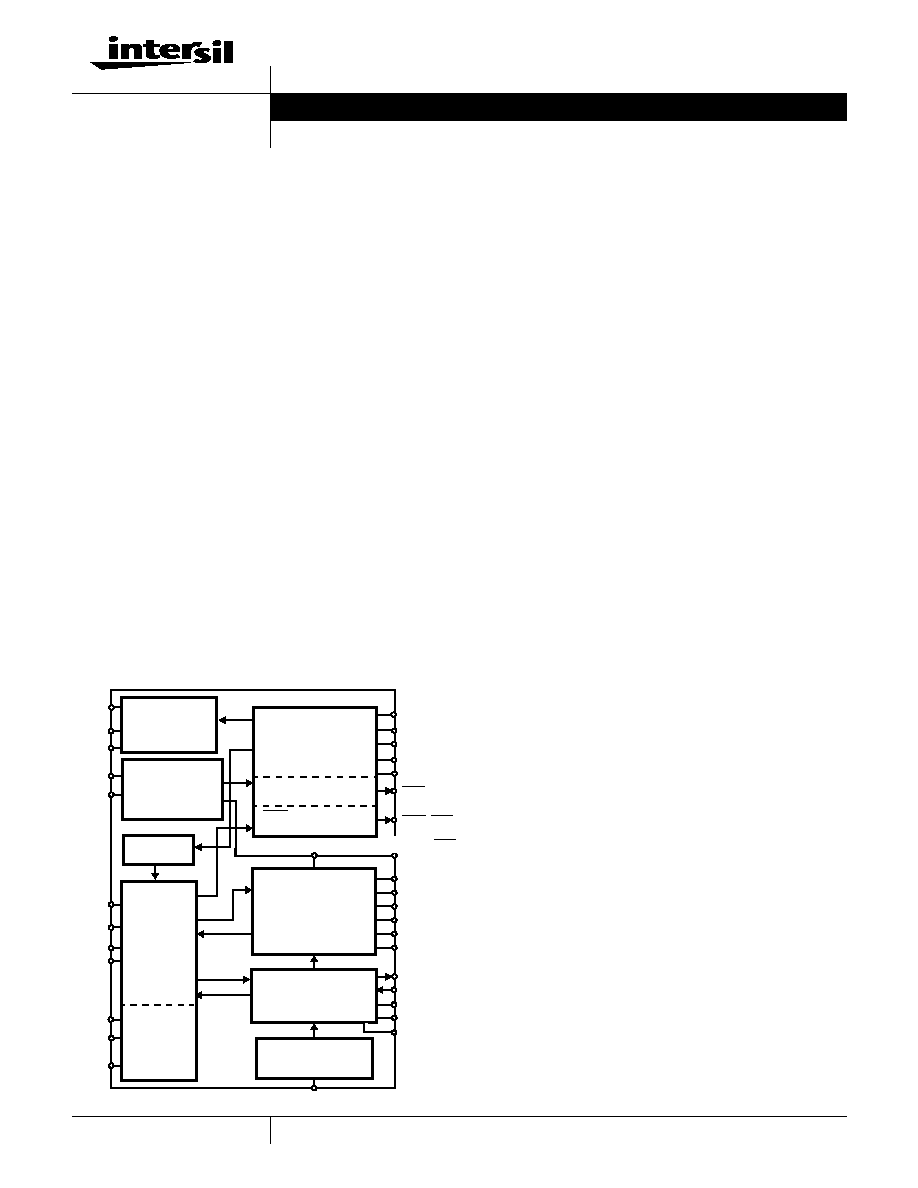
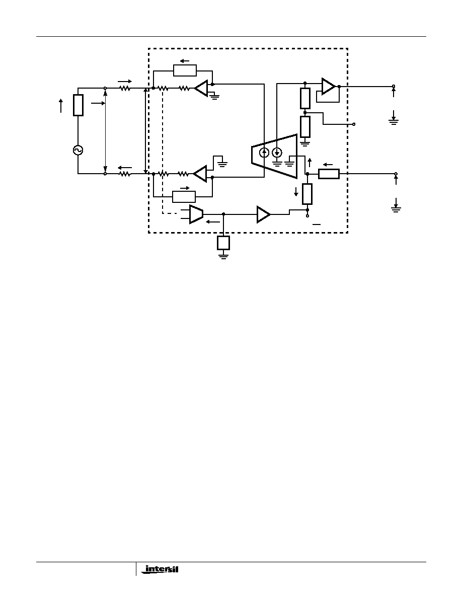
Block Diagram
Features
∑ Ultra Low Active Power (OHT) < 60mW
∑ Single/Dual Battery Operation
∑ Automatic Silent Battery Selection
∑ Power Management/Shutdown
∑ Battery Tracking Anti Clipping
∑ Single 5V Supply with 3V Compatible Logic
∑ Zero Crossing Ring Control
- Zero Voltage On/Zero Current Off
∑ Tip/Ring Disconnect
∑ Pulse Metering Capability
∑ 4 Wire Loopback
∑ Programmable Current Feed
∑ Programmable Resistive Feed
∑ Programmable Loop Detect Threshold
∑ Programmable On-Hook and Off-Hook Overheads
∑ Programmable Overhead for Pulse Metering
∑ Programmable Polarity Reversal Time
∑ Selectable Transmit Gain 0dB/-6dB
∑ 2 Wire Impedance Set by Single Network
∑ Loop and Ground Key Detectors
∑ On-Hook Transmission
∑ Common Pinout
∑ HC55121
- Polarity Reversal
∑ HC55130
- -63dB Longitudinal Balance
∑ HC55140
- Polarity Reversal
- Ground Start
- Line Voltage Measurement
- 2 Wire Loopback
- -63dB Longitudinal Balance
∑ HC55142
- Polarity Reversal
- Ground Start
- Line Voltage Measurement
- 2.2V
RMS
Pulse Metering
- 2 Wire Loopback
∑ HC55150
- Polarity Reversal
- Line Voltage Measurement
- 2.2V
RMS
Pulse Metering
- 2 Wire Loopback
Applications
∑ Related Literature
- AN9871, User's Guide for UniSLIC14 Eval Board
RRLY
DT
DR
TIP
RING
V
BH
V
CC
RING AND TEST
RELAY DRIVERS
RING TRIP
DETECTOR
V
BL
BGND
BATTERY
SELECTION
AND
BIAS
NETWORK
ZERO CURRENT
2-WIRE
INTERFACE
CROSSING
TRLY1
TRLY2
V
TX
V
RX
C1
C2
C3
GKD_LVM
ROH
RD
CDC
RDC_RAC
ZT
C
H
LOOP CURRENT
DETECTOR
PTG
ILIM
STATE
DECODER
AND
DETECTOR
LOGIC
GKD/LOOP LENGTH
DETECTOR
RSYNC_REV
SHD
4-WIRE INTERFACE
VF SIGNAL PATH
LINE FEED
CONTROL
C4
C5
CRT_REV_LVM
POLARITY
REVERSAL
PULSE METERING
SPM
SIGNAL PATH
AGND
Data Sheet
June 2000

4-2
Ordering Information
PART
NUMBER
MAX
LOOP
CURRENT
(mA)
POLARITY
REVERSAL
GND
START
GND
KEY
LINE
VOLTAGE
MEASUREMENT
PULSE
METERING
2 TEST
RELAY
DRIVERS
2 WIRE
LOOP-
BACK
LONGITUDINAL
BALANCE
TEMP
RANGE
(
o
C)
PKG.
NO.
HC55120CB
30
∑
53dB
0 to 70 M28.3
SOIC
HC55120CM
30
∑
53dB
0 to 70 N28.45
PLCC
HC55121IB
30
∑
∑
∑
∑
53dB
-40 to
85
M28.3
SOIC
HC55121IM
30
∑
∑
∑
∑
53dB
-40 to
85
N28.45
PLCC
HC55130IB
45
63dB
-40 to
85
M28.3
SOIC
HC55130IM
45
63dB
-40 to
85
N28.45
PLCC
HC55131IM
45
∑
63dB
-40 to
85
N32.45x55
PLCC
HC55140IB
45
∑
∑
∑
∑
∑
63dB
-40 to
85
M28.3
SOIC
HC55140IM
45
∑
∑
∑
∑
∑
63dB
-40 to
85
N28.45
PLCC
HC55141IM
45
∑
∑
∑
∑
∑
∑
63dB
-40 to
85
N32.45x55
PLCC
HC55142IB
45
∑
∑
∑
∑
∑
∑
63dB
-40 to
85
M28.3
SOIC
HC55142IM
45
∑
∑
∑
∑
∑
∑
63dB
-40 to
85
N28.45
PLCC
HC55143IM
45
∑
∑
∑
∑
∑
∑
∑
63dB
-40 to
85
N32.45x55
PLCC
HC55150CB
45
∑
∑
∑
∑
55dB
0 to 70 M28.3
SOIC
HC55150CM
45
∑
∑
∑
∑
55dB
0 to 70 N28.45
PLCC
HC55151CM
45
∑
∑
∑
∑
∑
55dB
0 to 70 N32.45x55
PLCC
HC5514XEVAL1 Evaluation board
Available by placing SLIC in Test mode.
Device Operating Modes
C3
C2
C1
DESCRIPTION
HC55120
HC55121
HC55130/1
HC55140/1
HC55142/3
HC55150/1
0
0
0
Open Circuit
4-Wire Loopback
∑
∑
∑
∑
∑
∑
0
0
1
Ringing
∑
∑
∑
∑
∑
∑
0
1
0
Forward Active
∑
∑
∑
∑
∑
∑
0
1
1
Test Forward Active
2 Wire Loopback and
Line Voltage Measurement
∑
∑
∑
∑
1
0
0
Tip Open Ground Start
∑
∑
1
0
1
Reserved
∑
∑
∑
∑
∑
∑
1
1
0
Reverse Active
∑
∑
∑
∑
1
1
1
Test Reverse Active
Line Voltage Measurement
∑
∑
∑
HC55120, HC55121, HC55130, HC55131, HC55140, HC55141, HC55142, HC55143, HC55150, HC55151
4-3
Absolute Maximum Ratings
T
A
= 25
o
C
Thermal Information
Temperature, Humidity
Storage Temperature Range . . . . . . . . . . . . . . . . -65
o
C to 150
o
C
Operating Temperature Range . . . . . . . . . . . . . . . -40
o
C to 110
o
C
Operating Junction Temperature Range. . . . . . . . -40
o
C to 150
o
C
Power Supply (-40
o
C
T
A
85
o
C)
Supply Voltage V
CC
to GND . . . . . . . . . . . . . . . . . . . . -0.4V to 7V
Supply Voltage V
BL
to GND . . . . . . . . . . . . . . . . . . . .-V
BH
to 0.4V
Supply Voltage V
BH
to GND, Continuous. . . . . . . . . . -75V to 0.4V
Supply Voltage V
BH
to GND, 10ms . . . . . . . . . . . . . . -80V to 0.4V
Relay Driver
Ring Relay Supply Voltage . . . . . . . . . . . . . . . . . . . . . . 0V to 14V
Ring Relay Current . . . . . . . . . . . . . . . . . . . . . . . . . . . . . . . . 50mA
Digital Inputs, Outputs (C1, C2, C3, C4, C5, SHD, GKD_LVM)
Input Voltage . . . . . . . . . . . . . . . . . . . . . . . . . . . . . . -0.4V to V
CC
Output Voltage (SHD, GKD_LVM Not Active). . . . . . -0.4V to V
CC
Output Current (SHD, GKD_LVM) . . . . . . . . . . . . . . . . . . . . . 5mA
ESD Rating . . . . . . . . . . . . . . . . . . . . . . . . . . . . . . . . . . . . . . . .500V
Gate Count. . . . . . . . . . . . . . . . . . . . . . . .543 Transistors, 51 Diodes
Tipx and Ringx Terminals (-40
o
C
T
A
85
o
C)
Tipx or Ringx Current . . . . . . . . . . . . . . . . . . . . -100mA to 100mA
Thermal Resistance (Typical, Note 1)
JA
28 Lead PLCC Package . . . . . . . . . . . . . . . . . . . . . .
52
o
C/W
28 Lead SOIC Package . . . . . . . . . . . . . . . . . . . . . .
45
o
C/W
32 Lead PLCC Package . . . . . . . . . . . . . . . . . . . . . .
66.2
o
C/W
Continuous Power Dissipation at 85
o
C
28 Lead PLCC Package . . . . . . . . . . . . . . . . . . . . . . . . . . . . .1.5W
28 Lead SOIC Package . . . . . . . . . . . . . . . . . . . . . . . . . . . . .2.0W
32 Lead PLCC Package . . . . . . . . . . . . . . . . . . . . . . . . . . . . .1.4W
Lead Temperature (Soldering 10s) . . . . . . . . . . . . . . . . . . . . . . . . 300
o
C
(PLCC, SOIC - Lead Tips Only)
Derate above 70
o
C
Tip and Ring Terminals
Tipx or Ringx, Current, Pulse < 10ms, T
REP
> 10s . . . . . . . . . .2A
Tipx or Ringx, Current, Pulse < 1ms, T
REP
> 10s . . . . . . . . . . .5A
Tipx or Ringx, Current, Pulse < 10
µ
s, T
REP
> 10s . . . . . . . . .15A
Tipx or Ringx, Current, Pulse < 1
µ
s, T
REP
> 10s . . . . . . . . . .20A
Tipx or Ringx, Pulse < 250ns, T
REP
> 10s
20A
CAUTION: Stresses above those listed in "Absolute Maximum Ratings" may cause permanent damage to the device. This is a stress only rating and operation of the
device at these or any other conditions above those indicated in the operational sections of this specification is not implied.
NOTE:
1.
JA
is measured with the component mounted on an evaluation PC board in free air.
Typical Operating Conditions
These represent the conditions under which the device was developed and are suggested as guidelines.
PARAMETER
CONDITIONS
MIN
TYP
MAX
UNITS
Ambient Temperature
HC55120, HC55150/1
0
-
70
o
C
HC55121, HC55130/1, HC55140/1,
HC55142/3
-40
-
85
o
C
V
BH
with Respect to GND
-58
-
-8
V
V
BL
with Respect to GND
V
BH
-
0
V
V
CC
with Respect to GND
4.75
-
5.25
V
HC55120, HC55121, HC55130, HC55131, HC55140, HC55141, HC55142, HC55143, HC55150, HC55151
4-4
Electrical Specifications
T
A
= -40
o
C to 85
o
C, V
CC
= +5V
±
5%, V
BH
= -48V, V
BL
= -24V, PTG = Open, R
P1
= R
P2
= 0
,
Z
T
= 120k
, R
LIM
= 38.3k
, R
D
= 50k
, RDC_RAC = 20k
,
R
OH
= 40k
, C
H
= 0.1
µ
F, C
DC
= 4.7
µ
F, C
RT/REV
= 0.47
µ
F, GND = 0V, RL = 600
. Unless Otherwise Specified.
(∑)
Symbol used to indicate the test applies
to the part. (NA) symbol used to indicate the test does not apply to the part.
PARAMETER
TEST CONDITIONS
MIN
TYP
MAX
UNITS
HC55120
HC55121
HC55130/1
HC55140/1
HC55142/3
HC55150/1
2-WIRE PORT
Overload Level, Off Hook
Forward and Reverse
1% THD, I
DCMET
18mA
(Note 2, Figure 1)
3.2
-
-
V
PEAK
Forward
Only
∑
Forward
Only
∑
∑
∑
Overload Level, On Hook
Forward and Reverse
1% THD, IDCMET
5mA
(Note 3, Figure 1)
1.3
-
-
V
PEAK
Forward
Only
∑
Forward
Only
∑
∑
∑
Input Impedance (Into Tip and Ring)
-
Z
T
/200
-
∑
∑
∑
∑
∑
∑
Longitudinal Impedance (Tip, Ring)
Forward and Reverse
0 < f < 100Hz (Note 4, Figure 2)
-
0
-
/Wire
Forward
Only
∑
Forward
Only
∑
∑
∑
LONGITUDINAL CURRENT LIMIT (TIP, RING)
On-Hook, Off-Hook (Active),
R
L
= 736
Forward and Reverse
No False Detections, (Loop
Current), LB > 45dB (Notes 5, 6,
Figures 3A, 3B)
28
-
-
mARMS
/
Wire
Forward
Only
∑
Forward
Only
∑
∑
∑
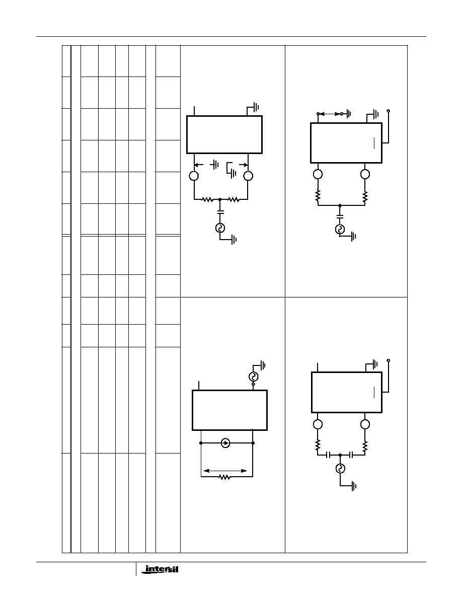
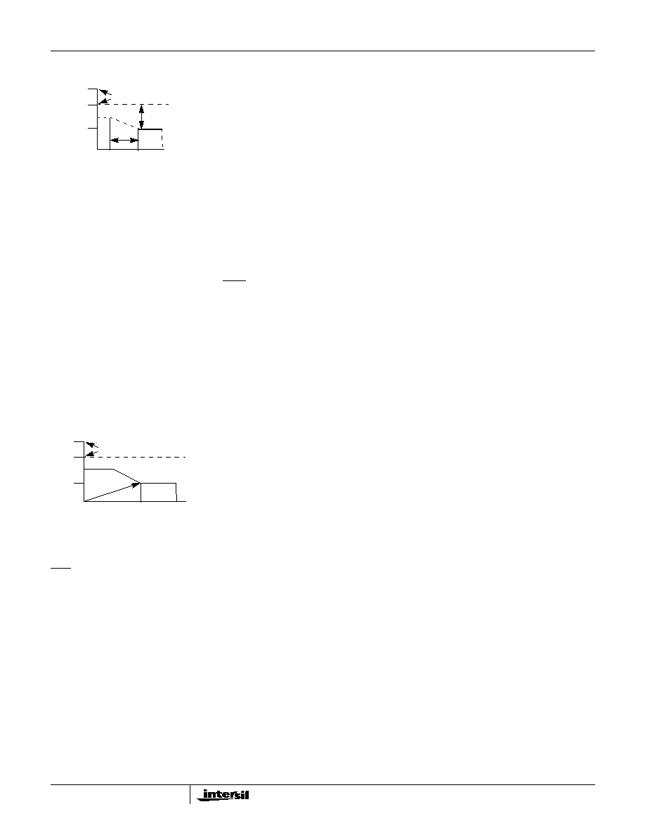
FIGURE 1. OVERLOAD LEVEL (OFF HOOK, ON HOOK)
FIGURE 2. LONGITUDINAL IMPEDANCE
FIGURE 3A. LONGITUDINAL CURRENT LIMIT ON-HOOK (ACTIVE)
FIGURE 3B. LONGITUDINAL CURRENT LIMIT OFF-HOOK (ACTIVE)
TIP
V
TX
RING
VRX
E
RX
R
L
V
TR
I
DCMET
E
L
V
T
C
0 < f < 100Hz
V
R
LZ
T
= V
T
/A
T
LZ
R
= V
R
/A
R
1V
RMS
300
300
TIP
RING
A
T
A
R
V
TX
VRX
E
L
368
368
A
TIP
RING
SHD
C
10
µ
F
C
10
µ
F
A
V
TX
VRX
E
L
368
368
C
A
TIP
RING
SHD
A
V
TX
VRX
V
TX
HC55120,
HC55121,
HC55130,
HC55131,
HC55140,
HC55141,
HC55142,
HC55143,
HC55150,
HC55151
4-5
OFF-HOOK LONGITUDINAL BALANCE
MIN
MIN
MIN
MIN
MIN
MIN
Longitudinal to Metallic (Note 7)
Forward and Reverse
IEEE 455 - 1985, R
LR
, R
LT
= 368
Normal Polarity:
Forward
Only
Forward
Only
0.2kHz < f < 1.0kHz, 0
o
C to 70
o
C
-
-
-
dB
53
NA
NA
NA
NA
55
1.0kHz < f < 3.4kHz, 0
o
C to 70
o
C
-
-
-
dB
53
NA
NA
NA
NA
55
0.2kHz < f < 1.0kHz, -40
o
C to 85
o
C
-
-
-
dB
NA
53
63
63
63
NA
1.0kHz < f < 3.4kHz, -40
o
C to 85
o
C
-
-
-
dB
NA
53
58
58
58
NA
Reverse Polarity 0.2kHz < f < 3.4kHz,
(Figure 4)
-
-
-
dB
NA
53
NA
58
58
55
MIN
MIN
MIN
MIN
MIN
MIN
Longitudinal to Metallic (Note 7)
Forward and Reverse
R
LR
, R
LT
= 300
,
Normal Polarity:
Forward
Only
Forward
Only
0.2kHz < f < 1.0kHz, 0
o
C to 70
o
C
-
-
-
dB
53
NA
NA
NA
NA
55
1.0kHz < f < 3.4kHz, 0
o
C to 70
o
C
-
-
-
dB
53
NA
NA
NA
NA
55
0.2kHz < f < 1.0kHz, -40
o
C to 85
o
C
-
-
-
dB
NA
53
63
63
63
NA
1.0kHz < f < 3.4kHz, -40
o
C to 85
o
C
-
-
-
dB
NA
53
58
58
58
NA
Reverse Polarity 0.2kHz < f < 3.4kHz,
(Figure 4)
-
-
-
dB
NA
53
NA
58
58
55
MIN
MIN
MIN
MIN
MIN
MIN
Longitudinal to 4-Wire (Note 9)
(Forward and Reverse)
Normal Polarity:
Forward
Only
Forward
Only
0.2kHz < f < 1.0kHz, 0
o
C to 70
o
C
-
-
-
dB
53
NA
NA
NA
NA
61
1.0kHz < f < 3.4kHz, 0
o
C to 70
o
C
-
-
-
dB
53
NA
NA
NA
NA
61
0.2kHz < f < 1.0kHz, -40
o
C to 85
o
C
-
-
-
dB
NA
53
63
63
63
NA
1.0kHz < f < 3.4kHz, -40
o
C to 85
o
C
-
-
-
dB
NA
53
58
58
58
NA
Reverse Polarity 0.2kHz < f < 3.4kHz,
(Figure 4)
-
-
dB
NA
53
NA
58
58
61
Metallic to Longitudinal (Note 10)
Forward and Reverse
FCC Part 68, Para 68.310 (Note 8)
0.2kHz < f < 3.4kHz, (Figure 5)
40
50
-
dB
Forward
Only
∑
Forward
Only
∑
∑
∑
4-Wire to Longitudinal (Note 11)
Forward and Reverse
0.2kHz < f < 3.4kHz, (Figure 5)
40
-
-
dB
Forward
Only
∑
Forward
Only
∑
∑
∑
Electrical Specifications
T
A
= -40
o
C to 85
o
C, V
CC
= +5V
±
5%, V
BH
= -48V, V
BL
= -24V, PTG = Open, R
P1
= R
P2
= 0
,
Z
T
= 120k
, R
LIM
= 38.3k
, R
D
= 50k
, RDC_RAC = 20k
,
R
OH
= 40k
, C
H
= 0.1
µ
F, C
DC
= 4.7
µ
F, C
RT/REV
= 0.47
µ
F, GND = 0V, RL = 600
. Unless Otherwise Specified.
(∑)
Symbol used to indicate the test applies
to the part. (NA) symbol used to indicate the test does not apply to the part. (Continued)
PARAMETER
TEST CONDITIONS
MIN
TYP
MAX
UNITS
HC55120
HC55121
HC55130/1
HC55140/1
HC55142/3
HC55150/1
HC55120,
HC55121,
HC55130,
HC55131,
HC55140,
HC55141,
HC55142,
HC55143,
HC55150,
HC55151
4-6
FIGURE 4. LONGITUDINAL TO METALLIC AND LONGITUDINAL TO 4-WIRE BALANCE
FIGURE 5. METALLIC TO LONGITUDINAL AND 4-WIRE TO LONGITUDINAL
BALANCE
2-Wire Return Loss
Forward and Reverse
0.2kHz to 1.0kHz (Note 12, Figure 6)
30
35
-
dB
Forward
Only
∑
Forward
Only
∑
∑
∑
1.0kHz to 3kHz (Note 12, Figure 6)
23
25
-
dB
3kHz to 3.4kHz (Note 12, Figure 6)
21
23
-
dB
TIP IDLE VOLTAGE (User Programmable)
TIPX Idle Voltage
Active, I
L
< 5mA
-2.6
-2.2
-1.8
V
Forward
Only
∑
Forward
Only
∑
∑
∑
Forward and Reverse
RING IDLE VOLTAGE (User Programmable)
RINGX Idle Voltage
Forward and Reverse
Active, I
L
< 5mA
-46.4
-45.3
-44.2
V
Forward
Only
∑
Forward
Only
∑
∑
∑
Tip open, I
L
< 5mA
-46.4
-45.3
-44.2
V
V
TR
Forward and Reverse
Active, I
L
< 5mA
41
43.1
45
V
Forward
Only
∑
Forward
Only
∑
∑
∑
V
TR(ROH)
Pulse Metering
Forward and Reverse
Active, I
L
8.5mA, R
OH
= 50k
36
38.1
-
V
NA
∑
NA
NA
∑
∑
FIGURE 6. TWO-WIRE RETURN LOSS
FIGURE 7. OVERLOAD LEVEL (4-WIRE TRANSMIT PORT), OUTPUT OFFSET
VOLTAGE AND HARMONIC DISTORTION
Electrical Specifications
T
A
= -40
o
C to 85
o
C, V
CC
= +5V
±
5%, V
BH
= -48V, V
BL
= -24V, PTG = Open, R
P1
= R
P2
= 0
,
Z
T
= 120k
, R
LIM
= 38.3k
, R
D
= 50k
, RDC_RAC = 20k
,
R
OH
= 40k
, C
H
= 0.1
µ
F, C
DC
= 4.7
µ
F, C
RT/REV
= 0.47
µ
F, GND = 0V, RL = 600
. Unless Otherwise Specified.
(∑)
Symbol used to indicate the test applies
to the part. (NA) symbol used to indicate the test does not apply to the part. (Continued)
PARAMETER
TEST CONDITIONS
MIN
TYP
MAX
UNITS
HC55120
HC55121
HC55130/1
HC55140/1
HC55142/3
HC55150/1
E
L
V
TR
C
R
LT
R
LR
2.16
µ
F
TIP
RING
V
TX
VRX
V
TX
E
TR
V
L
C
R
LT
R
LR
300
300
2.16
µ
F
TIP
RING
V
TX
VRX
E
RX
V
S
Z
D
R
LR
R
R
Z
IN
V
M
TIP
RING
V
TX
VRX
E
G
R
L
Z
L
V
TR
TIP
RING
V
TX
VRX
V
TX
600
HC55120,
HC55121,
HC55130,
HC55131,
HC55140,
HC55141,
HC55142,
HC55143,
HC55150,
HC55151
4-7
4-WIRE TRANSMIT PORT (V
TX
)
Overload Level, Off Hook (I
L
18mA)
Forward and Reverse
(Z
L
> 20k
, IL 1% THD) (Note 13,
Figure 7) T
A
= 0
o
C to 85
o
C
T
A
= -40
o
C to 0
o
C
3.2
-
-
V
PEAK
Forward
Only
∑
Forward
Only
∑
∑
∑
3.0
-
-
V
PEAK
Overload Level, On Hook (I
L
5mA)
Forward and Reverse
(Z
L
> 20k
, 1% THD)
(Note 14, Figure 7)
1.3
-
-
V
PEAK
Forward
Only
∑
Forward
Only
∑
∑
∑
V
TX
Output Offset Voltage
Forward and Reverse
E
G
= 0, Z
L
=
, (Note 15, Figure 7)
-200
-
200
mV
Forward
Only
∑
Forward
Only
∑
∑
∑
Output Impedance
(Guaranteed by Design)
0.2kHz < f < 03.4kHz
-
0.1
1
∑
∑
∑
∑
∑
∑
4-WIRE RECEIVE PORT (VRX)
VRX Input Impedance
(Guaranteed by Design)
0.2kHz < f < 3.4kHz
-
500
600
k
∑
∑
∑
∑
∑
∑
FREQUENCY RESPONSE (OFF-HOOK)
2-Wire to 4-Wire
Forward and Reverse
Relative to 0dBm at 1.0kHz, E
RX
= 0V
Forward
Only
∑
Forward
Only
∑
∑
∑
0.3kHz < f < 3.4kHz
-0.15
-
0.15
dB
f = 8.0kHz (Note 16, Figure 8)
-
0.24
0.5
dB
f = 12kHz (Note 16, Figure 8)
-
0.58
1.0
dB
f = 16kHz (Note 16, Figure 8)
-
1.0
1.5
dB
4-Wire to 2-Wire
Forward and Reverse
Relative to 0dBm at 1.0kHz, E
G
= 0V
0.3kHz < f < 3.4kHz
-0.15
-
0.15
dB
Forward
Only
∑
Forward
Only
∑
∑
∑
f = 8kHz (Note 17, Figure 8)
-0.5
0.24
-
dB
f = 12kHz (Note 17, Figure 8)
-1.0
0.58
-
dB
f = 16kHz (Note 17, Figure 8)
-1.5
1.0
-
dB
4-Wire to 4-Wire
Forward and Reverse
Relative to 0dBm at 1.0kHz, E
G
= 0V
Forward
Only
∑
Forward
Only
∑
∑
∑
0.3kHz < f < 3.4kHz (Note 18, Figure 8) -0.15
-
0.15
dB
8kHz, 12kHz, 16kHz (Note 18, Figure 8)
-0.5
0
0.5
dB
FIGURE 8. FREQUENCY RESPONSE, INSERTION LOSS, GAIN TRACKING
AND HARMONIC DISTORTION
FIGURE 9. IDLE CHANNEL NOISE
Electrical Specifications
T
A
= -40
o
C to 85
o
C, V
CC
= +5V
±
5%, V
BH
= -48V, V
BL
= -24V, PTG = Open, R
P1
= R
P2
= 0
,
Z
T
= 120k
, R
LIM
= 38.3k
, R
D
= 50k
, RDC_RAC = 20k
,
R
OH
= 40k
, C
H
= 0.1
µ
F, C
DC
= 4.7
µ
F, C
RT/REV
= 0.47
µ
F, GND = 0V, RL = 600
. Unless Otherwise Specified.
(∑)
Symbol used to indicate the test applies
to the part. (NA) symbol used to indicate the test does not apply to the part. (Continued)
PARAMETER
TEST CONDITIONS
MIN
TYP
MAX
UNITS
HC55120
HC55121
HC55130/1
HC55140/1
HC55142/3
HC55150/1
E
G
R
L
600
V
TR
E
RX
TIP
RING
VRX
V
TX
V
TX
PTG
OPEN
600
V
TR
R
L
TIP
RING
VRX
V
TX
V
TX
HC55120,
HC55121,
HC55130,
HC55131,
HC55140,
HC55141,
HC55142,
HC55143,
HC55150,
HC55151
4-8
INSERTION LOSS
2-Wire to 4-Wire
Forward and Reverse
0dBm, 1kHz
∑
∑
∑
∑
PTG = Open (Note 19, Figure 8)
-0.2
-
0.2
dB
Forward
Only
Forward
Only
PTG = GND (Note 20, Figure 8)
-6.22
-6.02
-5.82
dB
4-Wire to 2-Wire
Forward and Reverse
0dBm, 1kHz (Note 21, Figure 8)
-0.2
-
0.2
dB
Forward
Only
∑
Forward
Only
∑
∑
∑
GAIN TRACKING (Ref = -10dBm, at 1.0kHz)
2-Wire to 4-Wire
Forward and Reverse
-40dBm to +3dBm (Note 22, Figure 8)
-0.1
-
0.1
dB
Forward
Only
∑
Forward
Only
∑
∑
∑
-55dBm to -40dBm (Note 22, Figure 8)
-0.2
-
0.2
dB
4-Wire to 2-Wire
Forward and Reverse
-40dBm to +3dBm (Note 23, Figure 8)
-0.1
-
0.1
dB
Forward
Only
∑
Forward
Only
∑
∑
∑
-55dBm to -40dBm (Note 23, Figure 8)
-0.2
-
0.2
dB
NOISE
Idle Channel Noise at 2-Wire
C-Message Weighting
-
10.5
13
dBrnC
Forward
Only
∑
Forward
Only
∑
∑
∑
Forward and Reverse
Psophometric Weighting (Note 24,
Note 30, Figure 9)
-
-79.5
-77
dBmp
Idle Channel Noise at 4-Wire
C-Message Weighting
-
10.5
13
dBrnC
Forward
Only
∑
Forward
Only
∑
∑
∑
Forward and Reverse
Psophometrical Weighting
(Note 25, Note 30, Figure 9)
-
-79.5
-77
dBmp
HARMONIC DISTORTION
2-Wire to 4-Wire
Forward and Reverse
0dBm, 0.3kHz to 3.4kHz
(Note 26, Figure 7)
-
-67
-50
dB
Forward
Only
∑
Forward
Only
∑
∑
∑
4-Wire to 2-Wire
Forward and Reverse
0dBm, 0.3kHz to 3.4kHz
(Note 27, Figure 8)
-
-67
-50
dB
Forward
Only
∑
Forward
Only
∑
∑
∑
FIGURE 10. CONSTANT LOOP CURRENT TOLERANCE
FIGURE 11. TIPX VOLTAGE
Electrical Specifications
T
A
= -40
o
C to 85
o
C, V
CC
= +5V
±
5%, V
BH
= -48V, V
BL
= -24V, PTG = Open, R
P1
= R
P2
= 0
,
Z
T
= 120k
, R
LIM
= 38.3k
, R
D
= 50k
, RDC_RAC = 20k
,
R
OH
= 40k
, C
H
= 0.1
µ
F, C
DC
= 4.7
µ
F, C
RT/REV
= 0.47
µ
F, GND = 0V, RL = 600
. Unless Otherwise Specified.
(∑)
Symbol used to indicate the test applies
to the part. (NA) symbol used to indicate the test does not apply to the part. (Continued)
PARAMETER
TEST CONDITIONS
MIN
TYP
MAX
UNITS
HC55120
HC55121
HC55130/1
HC55140/1
HC55142/3
HC55150/1
600
V
TR
R
L
TIP
RING
V
TX
VRX
R
LIM
R
LIM
38.3k
TIP
RING
S
R
1
7k
V
BH
V
TX
VRX
I
R1
HC55120,
HC55121,
HC55130,
HC55131,
HC55140,
HC55141,
HC55142,
HC55143,
HC55150,
HC55151
4-9
BATTERY FEED CHARACTERISTICS
Constant Loop Current Tolerance
18mA
IL
45mA,
Forward
Only
∑
Forward
Only
∑
∑
∑
I
L
= 26.5mA, R
LIM
= 38.3k
Forward and Reverse
(Note 27, Figure 10)
0.92I
L
I
L
1.08I
L
mA
Tip Open State TIPX Leakage
Current
S = Closed (Figure 11)
-
-
-200
µ
A
∑
∑
∑
∑
∑
∑
Tip Open State RINGX Current
R
1
= 0
, V
BH
= -48V, R
LIM
= 38.3k
22.6
26.8
31
mA
∑
∑
∑
∑
∑
∑
R
1
= 2.5k
, V
BH
= -48V (Figure 11)
15.5
17.1
18.2
mA
Tip Open State RINGX Voltage
5mA < I
R1
< 26mA (Figure 11)
-
42.8
-
V
∑
∑
∑
∑
∑
∑
Tip Voltage (Ground Start)
Active State, (S Open) R
1
= 150
(Figure 11)
-5.3
-4.8
-4.3
V
NA
NA
NA
∑
∑
NA
Tip Voltage (Ground Start)
Active State, (S Closed) Tip Lead to
∑
∑
-48V Through 7k
, Ring Lead to
Ground Through 150
(Figure 11)
-5.3
-4.8
-4.3
V
NA
NA
NA
NA
Open Circuit State Loop Current
(Active) R
L
= 0
-20
0
20
µ
A
∑
∑
∑
∑
∑
∑
LOOP CURRENT DETECTOR
Programmable Threshold
I
LTh
= (500/ R
D
)
5mA,
0.9I
LTh
I
LTh
1.1I
LTh
mA
Forward
Only
∑
Forward
Only
∑
∑
∑
Forward and Reverse
I
LTh
= 8.5mA
R
D
= 58.8k
GROUND KEY DETECTOR
Ground Key Detector Threshold
Tip/Ring Current Difference
Tip Open
5
8
11
mA
∑
∑
NA
∑
∑
NA
Active (Note 29, R1 = 2.5k
, Figure 12)
12.5
20
27.5
mA
LINE VOLTAGE MEASUREMENT
Pulse Width (GKD_LVM)
Pulse Width = (20)(C
REV...
/I
LIM
)
0.32
0.36
0.4
ms/V
NA
NA
NA
∑
∑
∑
RING TRIP DETECTOR (DT, DR)
Ring Trip Comparator Current
Source Res = 2M
-
2
-
µ
A
∑
∑
∑
∑
∑
∑
Input Common-Mode Range
Source Res = 2M
-
-
±
200
V
∑
∑
∑
∑
∑
∑
Electrical Specifications
T
A
= -40
o
C to 85
o
C, V
CC
= +5V
±
5%, V
BH
= -48V, V
BL
= -24V, PTG = Open, R
P1
= R
P2
= 0
,
Z
T
= 120k
, R
LIM
= 38.3k
, R
D
= 50k
, RDC_RAC = 20k
,
R
OH
= 40k
, C
H
= 0.1
µ
F, C
DC
= 4.7
µ
F, C
RT/REV
= 0.47
µ
F, GND = 0V, RL = 600
. Unless Otherwise Specified.
(∑)
Symbol used to indicate the test applies
to the part. (NA) symbol used to indicate the test does not apply to the part. (Continued)
PARAMETER
TEST CONDITIONS
MIN
TYP
MAX
UNITS
HC55120
HC55121
HC55130/1
HC55140/1
HC55142/3
HC55150/1
HC55120,
HC55121,
HC55130,
HC55131,
HC55140,
HC55141,
HC55142,
HC55143,
HC55150,
HC55151
4-10
RING RELAY DRIVER
V
SAT
at 30mA
I
OL
= 30mA
-
0.2
0.5
V
∑
∑
∑
∑
∑
∑
V
SAT
at 40mA
I
OL
= 40mA
-
0.52
0.8
V
∑
∑
∑
∑
∑
∑
Off State Leakage Current
V
OH
= 13.2V
-
0.1
10
µ
A
∑
∑
∑
∑
∑
∑
TEST RELAY DRIVER (TRLY1, TRLY2)
V
SAT
at 30mA
I
OL
= 30mA
-
0.3
0.5
V
NA
NA
NA/
∑
NA/
∑
NA/
∑
NA/
∑
V
SAT
at 40mA
I
OL
= 40mA
-
0.62
0.9
V
NA
NA
NA/
∑
NA/
∑
NA/
∑
NA/
∑
Off State Leakage Current
V
OH
= 13.2V
-
-
10
µ
A
NA
NA
NA/
∑
NA/
∑
NA/
∑
NA/
∑
FIGURE 12. GROUND KEY DETECT
DIGITAL INPUTS (C1, C2, C3)
Input Low Voltage, V
IL
0
-
0.8
V
∑
∑
∑
∑
∑
∑
Input High Voltage, V
IH
2.0
-
V
CC
V
∑
∑
∑
∑
∑
∑
Input Low Current, I
IL
V
IL
= 0.4V
-
-
-10
µ
A
∑
∑
∑
∑
∑
∑
Input High Current, I
IH
V
IH
= 2.5V
-
25
50
µ
A
∑
∑
∑
∑
∑
∑
DETECTOR OUTPUTS (SHD, GKD_LVM)
SHD Output Low Voltage, V
OL
Forward, Reverse
I
OL
= 1mA
-
-
0.5
V
Forward
Only
∑
Forward
Only
∑
∑
∑
SHD Output High Voltage, V
OH
Forward, Reverse
I
OH
= 100
µ
A
2.7
-
-
V
Forward
Only
∑
Forward
Only
∑
∑
∑
GKD_LVM Output Low Voltage,
V
OL
Forward and Tip Open
I
OL
= 1mA
R
1
= 2.5k
(Figure 11)
-
-
0.5
V
GKD
GKD
NA
GKD_
LVM
GKD_
LVM
LVM
GKD_LVM Output High Voltage,
V
OH
Forward and Tip Open
I
OH
= 100
µ
A
2.7
-
-
V
GKD
GKD
NA
GKD_
LVM
GKD_
LVM
LVM
Internal Pull-Up Resistor
-
15
-
k
∑
∑
∑
∑
∑
∑
Electrical Specifications
T
A
= -40
o
C to 85
o
C, V
CC
= +5V
±
5%, V
BH
= -48V, V
BL
= -24V, PTG = Open, R
P1
= R
P2
= 0
,
Z
T
= 120k
, R
LIM
= 38.3k
, R
D
= 50k
, RDC_RAC = 20k
,
R
OH
= 40k
, C
H
= 0.1
µ
F, C
DC
= 4.7
µ
F, C
RT/REV
= 0.47
µ
F, GND = 0V, RL = 600
. Unless Otherwise Specified.
(∑)
Symbol used to indicate the test applies
to the part. (NA) symbol used to indicate the test does not apply to the part. (Continued)
PARAMETER
TEST CONDITIONS
MIN
TYP
MAX
UNITS
HC55120
HC55121
HC55130/1
HC55140/1
HC55142/3
HC55150/1
TIP
RING
SHD
2.5k
V
TX
VRX
HC55120,
HC55121,
HC55130,
HC55131,
HC55140,
HC55141,
HC55142,
HC55143,
HC55150,
HC55151
4-11
POWER DISSIPATION (V
BH
= -48V, V
BL
= -24V)
Open Circuit State
C1, C2, C3 = 0, 0, 0
-
25
-
mW
Forward
Only
∑
Forward
Only
∑
∑
∑
On-Hook, Active
C1, C2, C3 = 0, 1, 0
C1, C2, C3 = 1, 1, 0
∑
∑
∑
∑
Forward and Reverse
I
L
= 0mA, Longitudinal
Current = 0mA
-
52
-
mW
Forward
Only
∑
Forward
Only
∑
∑
∑
POWER SUPPLY CURRENTS (V
BH
= -48V, V
BL
= -24V)
V
CC
Current, I
CC
Open Circuit State
-
2.25
3.0
mA
Forward
Only
∑
Forward
Only
∑
∑
∑
V
BH
Current, I
BH
-
0.3
0.45
mA
Forward
Only
∑
Forward
Only
∑
∑
∑
V
BL
Current, I
BL
-
0.022
0.035
mA
Forward
Only
∑
Forward
Only
∑
∑
∑
V
CC
Current, I
CC
Forward and Reverse
Active State
I
L
= 0mA, Longitudinal
Current = 0mA
-
2.7
3.6
mA
Forward
Only
∑
Forward
Only
∑
∑
∑
V
BH
Current, I
BH
Forward and Reverse
-
0.8
1.06
mA
Forward
Only
∑
Forward
Only
∑
∑
∑
V
BL
Current, I
BL
Forward and Reverse
-
-
0.01
mA
Forward
Only
∑
Forward
Only
∑
∑
∑
POWER SUPPLY REJECTION RATIOS
V
CC
to 2 or 4 Wire Port
Forward and Reverse
Active State R
L
= 600
50Hz < f < 3400Hz, V
IN
=100mV
-
40
-
dB
Forward
Only
∑
Forward
Only
∑
∑
∑
V
BH
to 2 or 4 Wire Port
Forward and Reverse
-
40
-
dB
Forward
Only
∑
Forward
Only
∑
∑
∑
V
BL
to 2 or 4 Wire Port
Forward and Reverse
-
40
-
dB
Forward
Only
∑
Forward
Only
∑
∑
∑
TEMPERATURE GUARD
Junction Threshold Temperature
-
175
-
o
C
∑
∑
∑
∑
∑
∑
Electrical Specifications
T
A
= -40
o
C to 85
o
C, V
CC
= +5V
±
5%, V
BH
= -48V, V
BL
= -24V, PTG = Open, R
P1
= R
P2
= 0
,
Z
T
= 120k
, R
LIM
= 38.3k
, R
D
= 50k
, RDC_RAC = 20k
,
R
OH
= 40k
, C
H
= 0.1
µ
F, C
DC
= 4.7
µ
F, C
RT/REV
= 0.47
µ
F, GND = 0V, RL = 600
. Unless Otherwise Specified.
(∑)
Symbol used to indicate the test applies
to the part. (NA) symbol used to indicate the test does not apply to the part. (Continued)
PARAMETER
TEST CONDITIONS
MIN
TYP
MAX
UNITS
HC55120
HC55121
HC55130/1
HC55140/1
HC55142/3
HC55150/1
HC55120,
HC55121,
HC55130,
HC55131,
HC55140,
HC55141,
HC55142,
HC55143,
HC55150,
HC55151

4-12
Notes
2. Overload Level (Two-Wire Port, Off Hook) - The overload
level is specified at the 2-wire port (V
TR
) with the signal source at
the 4-wire receive port (E
RX
). R
L
= 600
, I
DCMET
18mA.
Increase the amplitude of E
RX
until 1% THD is measured at V
TR
.
Reference Figure 1.
3. Overload Level (Two-Wire Port, On Hook) - The overload
level is specified at the 2-wire port (V
TR
) with the signal source at
the 4-wire receive port (E
RX
). R
L
=
, I
DCMET
= 0mA. Increase
the amplitude of E
RX
until 1% THD is measured at V
TR
.
Reference Figure 1.
4. Longitudinal Impedance - The longitudinal impedance is
computed using the following equations, where TIP and RING
voltages are referenced to ground. L
ZT
, L
ZR
, V
T
, V
R
, A
R
and A
T
are defined in Figure 2.
(TIP) L
ZT
= V
T
/A
T
(RING) L
ZR
= V
R
/A
R
where: E
L
= 1V
RMS
(0Hz to 100Hz)
5. Longitudinal Current Limit (On-Hook Active) - On-Hook
longitudinal current limit is determined by increasing the (60Hz)
amplitude of E
L
(Figure 3A) until the 2-wire longitudinal current
is greater than 28mARMS/Wire. Under this condition, SHD pin
remains low (no false detection) and the 2-wire to 4-wire
longitudinal balance is verified to be greater than 45dB
(LB
2-4
= 20log VTX/E
L
).
6. Longitudinal Current Limit (Off-Hook Active) - Off-Hook
longitudinal current limit is determined by increasing the (60Hz)
amplitude of E
L
(Figure 3B) until the 2-wire longitudinal current
is greater than 28mARMS/Wire. Under this condition, SHD pin
remains high (no false detection) and the 2-wire to 4-wire
longitudinal balance is verified to be greater than 45dB
(LB
2-4
= 20log VTX/E
L
).
7. Longitudinal to Metallic Balance - The longitudinal to
metallic balance is computed using the following equation:
BLME = 20 log (E
L
/V
TR
), where: E
L
and V
TR
are defined in
Figure 4.
8. Metallic to Longitudinal FCC Part 68, Para 68.310 - The
metallic to longitudinal balance is defined in this spec.
9. Longitudinal to Four-Wire Balance - The longitudinal to 4-wire
balance is computed using the following equation:
BLFE = 20 log (E
L
/V
TX
), E
L
and V
TX
are defined in Figure 4.
10. Metallic to Longitudinal Balance - The metallic to longitudinal
balance is computed using the following equation:
BMLE = 20 log (E
TR
/V
L
), E
RX
= 0
where: E
TR,
V
L
and E
RX
are defined in Figure 5.
11. Four-Wire to Longitudinal Balance - The 4-wire to longitudinal
balance is computed using the following equation:
BFLE = 20 log (E
RX
/V
L
), E
TR
= source is removed.
where: E
RX,
V
L
and E
TR
are defined in Figure 5.
12. Two-Wire Return Loss - The 2-wire return loss is computed
using the following equation:
r = -20 log (2V
M
/V
S
) where: Z
D
= The desired impedance; e.g.,
the characteristic impedance of the line, nominally 600
.
(Reference Figure 6).
13. Overload Level (4-Wire Port Off-Hook) - The overload level
is specified at the 4-wire transmit port (V
TX
) with the signal
source (E
G
) at the 2-wire port, Z
L
= 20k
,
R
L
= 600
(Reference Figure 7). Increase the amplitude of E
G
until 1%
THD is measured at V
TX
. Note the PTG pin is open, and the
gain from the 2-wire port to the 4-wire port is equal to 1.
14. Overload Level (4-Wire Port On-Hook) - The overload level is
specified at the 4-wire transmit port (V
TX
) with the signal source
(E
G
) at the 2-wire port, Z
L
= 20k
,
R
L
=
(Reference Figure 7).
Increase the amplitude of E
G
until 1% THD is measured at V
TX
.
Note the PTG pin is open, and the gain from the 2-wire port to
the 4-wire port is equal to 1.
15. Output Offset Voltage - The output offset voltage is specified
with the following conditions: E
G
= 0, R
L
= 600
, Z
L
=
and is
measured at V
TX
. E
G
, R
L
, V
TX
and Z
L
are defined in Figure 7.
16. Two-Wire to Four-Wire Frequency Response - The 2-wire to
4-wire frequency response is measured with respect to
E
G
= 0dBm at 1.0kHz, E
RX
= 0V (VRX input floating), R
L
= 600
.
The frequency response is computed using the following equation:
F
2-4
= 20 log (V
TX
/V
TR
), vary frequency from 300Hz to 3.4kHz
and compare to 1kHz reading.
V
TX
, V
TR
, R
L
and E
G
are defined in Figure 8.
17. Four-Wire to Two-Wire Frequency Response - The 4-wire to 2-
wire frequency response is measured with respect to E
RX
= 0dBm
at 1.0kHz, E
G
source removed from circuit, R
L
= 600
. The
frequency response is computed using the following equation:
F
4-2
= 20 log (V
TR
/E
RX
), vary frequency from 300Hz to 3.4kHz
and compare to 1kHz reading.
V
TR
, R
L
and E
RX
are defined in Figure 8.
18. Four-Wire to Four-Wire Frequency Response - The 4-wire
to 4-wire frequency response is measured with respect to
E
RX
= 0dBm at 1.0kHz, E
G
source removed from circuit,
R
L
= 600
. The frequency response is computed using the
following equation:
F
4-4
= 20 log (V
TX
/E
RX
), vary frequency from 300Hz to 3.4kHz
and compare to 1kHz reading.
V
TX ,
R
L
and E
RX
are defined in Figure 8.
19. Two-Wire to Four-Wire Insertion Loss (PTG = Open) - The
2-wire to 4-wire insertion loss is measured with respect to
E
G
= 0dBm at 1.0kHz input signal, E
RX
= 0 (VRX input floating),
R
L
= 600
and is computed using the following equation:
L
2-4
= 20 log (V
TX
/V
TR
)
where: V
TX
, V
TR
, R
L
and E
G
are defined in Figure 8. (Note:
The fuse resistors, R
F
, impact the insertion loss. The specified
insertion loss is for R
F1
= R
F2
= 0).
20. Two-Wire to Four-Wire Insertion Loss (PTG = AGND) - The
2-wire to 4-wire insertion loss is measured with respect to E
G
=
0dBm at 1.0kHz input signal, E
RX
= 0 (VRX input floating), R
L
=
600
and is computed using the following equation:
L
2-4
= 20 log (V
TX
/V
TR
)
where: V
TX
, V
TR
, R
L
and E
G
are defined in Figure 8. (Note:
The fuse resistors, R
F
, impact the insertion loss. The specified
insertion loss is for R
F1
= R
F2
= 0).
21. Four-Wire to Two-Wire Insertion Loss - The 4-wire to 2-wire
insertion loss is measured based upon E
RX
= 0dBm, 1.0kHz
input signal, E
G
source removed from circuit, R
L
= 600
and is
computed using the following equation:
L
4-2
= 20 log (V
TR
/E
RX
)
where: V
TR
, R
L
and E
RX
are defined in Figure 8.
22. Two-Wire to Four-Wire Gain Tracking - The 2-wire to 4-wire
gain tracking is referenced to measurements taken for
E
G
= -10dBm, 1.0kHz signal, E
RX
= 0 (VRX output floating),
R
L
= 600
and is computed using the following equation.
G
2-4
= 20
∑
log (V
TX
/V
TR
) vary amplitude -40dBm to +3dBm, or
-55dBm to -40dBm and compare to -10dBm reading.
V
TX
, R
L
and V
TR
are defined in Figure 8.
HC55120, HC55121, HC55130, HC55131, HC55140, HC55141, HC55142, HC55143, HC55150, HC55151

4-13
23. Four-Wire to Two-Wire Gain Tracking - The 4-wire to 2-wire
gain tracking is referenced to measurements taken for
E
RX
= -10dBm, 1.0kHz signal, E
G
source removed from circuit,
R
L
= 600
and is computed using the following equation:
G
4-2
= 20
∑
log (V
TR
/E
RX
) vary amplitude -40dBm to +3dBm,
or -55dBm to -40dBm and compare to -10dBm reading.
V
TR
, R
L
and E
RX
are defined in Figure 8. The level is specified at
the 4-wire receive port and referenced to a 600
impedance level.
24. Two-Wire Idle Channel Noise - The 2-wire idle channel noise
at V
TR
is specified with the 2-wire port terminated in 600
(R
L
)
and with the 4-wire receive port (VTX) floating (Reference
Figure 9).
25. Four-Wire Idle Channel Noise - The 4-wire idle channel noise
at V
TX
is specified with the 2-wire port terminated in 600
(R
L
).
The noise specification is with respect to a 600
impedance
level at V
TX
. The 4-wire receive port (VTX) floating (Reference
Figure 9).
26. Harmonic Distortion (2-Wire to 4-Wire) - The harmonic
distortion is measured within the voice band with the following
conditions. E
G
= 0dBm at 1kHz, R
L
= 600
. Measurement
taken at V
TX
. (Reference Figure 7).
27. Harmonic Distortion (4-Wire to 2-Wire) - The harmonic
distortion is measured within the voice band with the following
conditions. E
RX
= 0dBm0. Vary frequency between 300Hz and
3.4kHz, R
L
= 600
. Measurement taken at V
TR
. (Reference
Figure 8).
28. Constant Loop Current - The constant loop current is
calculated using the following equation:
I
L
= 1000/R
LIM
= V
TR
/600 (Reference Figure 10).
29. Ground Key Detector - (TRIGGER) Ground the Ring pin
through a 2.5k
resistor and verify that GKD goes low.
(RESET) Disconnect the Ring pin and verify that GKD goes
high.
(Hysteresis) Compare difference between trigger and reset.
30. Electrical Test - Not tested in production at -40
o
C.
Circuit Operation and Design Information
The UniSLIC14 family of SLICs are voltage feed current
sense Subscriber Line Interface Circuits (SLIC). For short
loop applications, the voltage between the tip and ring
terminals varies to maintain a constant loop current. For long
loop applications, the voltage between the tip and ring
terminals are relatively constant and the loop current varies
in proportion to the load.
The tip and ring voltages for various loop resistances are
shown in Figure 13. The tip voltage remains relatively
constant as the ring voltage moves to limit the loop current
for short loops.
The loop current for various loop resistances are shown in
Figure 14. For short loops, the loop current is limited to the
programmed current limit, set by RILIM. For long loop
applications, the loop current varies in accordance with
Ohms law for the given tip to ring voltage and the loop
resistance.
.
The following discussion separates the SLIC's operation into
its DC and AC paths, then follows up with additional circuit
and design information.
DC Feed Curve
The DC feed curve for the UniSLIC14 family is user
programmable. The user defines the on hook and off hook
overhead voltages (including the overhead voltage for off
hook pulse metering if applicable), the maximum and
minimum loop current limits, the switch hook detect
threshold and the battery voltage. From these requirements,
the DC feed curve is customized for optimum operation in
any given application. An Excel spread sheet to calculate the
external components can be downloaded off our web site
www.intersil.com/telecom/unislic14.xls.
FIGURE 13. TIP AND RING VOLTAGES vs LOOP RESISTANCE
TIP AND RING V
O
L
T
A
GES (V)
LOOP RESISTANCE (
)
0
-5
-10
-15
-20
-25
-30
-35
-50
-40
-45
200
600
1000 1400 1800 2000
4K
10K
6K
8K
CONSTANT
LOOP CURRENT
REGION
VBH = -48V
RD = 41.2k
ROH = 38.3k
RDC_RAC = 19.6k
RILim = 33.2k
CONSTANT TIP TO RING
VOLTAGE REGION
-44.5V
-2.5V
TIP
RING
FIGURE 14. LOOP CURRENT vs LOOP RESISTANCE
LOOP CURRENT (mA)
0
LOOP RESISTANCE (
)
200
600
1K
1.4K 1.8K
2.2K 2.6K
3.8K
3.0K 3.4K
35
30
25
20
15
10
5
CONSTANT
LOOP CURRENT
REGION
VBH = -48V
RD = 41.2k
ROH = 38.3k
RDC_RAC = 19.6k
RILim = 33.2k
CONSTANT TIP TO RING
VOLTAGE REGION
HC55120, HC55121, HC55130, HC55131, HC55140, HC55141, HC55142, HC55143, HC55150, HC55151
4-14
On Hook Overhead Voltage
The on hook overhead voltage
at the load (V
OH
(on) at Load)
is independent of the V
BH
battery voltage. Once set, the
on hook voltage remains
constant as the V
BH
battery
voltage changes. The on hook
voltage also remains constant
over temperature and line
leakages up to 0.6 times the
Switch Hook Detect threshold (I
SHD
). The maximum loop
current for a constant on hook overhead voltage is defined
as ISH-.
The on hook overhead voltage, required for a given signal
level at the load, must take into account the AC voltage drop
across the 2 external protection resistors (R
P
) and the 2
internal sense resistors (R
S
) as shown in Figure 16. The AC
on hook overload voltage is calculated using Equation 1.
where
V
OH(on) at Load
= On hook overhead voltage at load
V
sp(on)
= Required on hook transmission for speech
R
P
= Protection Resistors (Typically 30
)
R
S
= Internal Sense Resistors (40
)
Z
L
= AC load impedance for (600
)
1.5V = Additional on hook overhead voltage requirement
To account for any process and temperature variations in the
performance of the SLIC, 1.5V is added to the overhead
voltage requirement for the on hook case in Equation 1 and
2.0V for the off hook case in Equation 3. Note the 2.5V
overhead is automatically generated in the SLIC and is not
part of the external overhead programming.
Off Hook Overhead Voltage
The off hook overhead
voltage V
OH
(off) at Load is
also independent of the V
BH
battery voltage and remains
constant over temperature.
The required off hook
overhead voltage is the sum
of the AC and DC voltage
drops across the internal
sense resistors (R
S)
, the
Internal overhead voltage automatically generated by the SLIC.
FIGURE 15. UniSLIC14 DC FEED CURVE
VBH
2.5V
VOH(off) AT LOAD
ISH-
ILOOP(min)
ILOOP(max)
60k
SLOPE
RLOOP(max)
SLIC SELF PROGRAMMING
TIP T
O
RING ABSOLUTE V
O
L
T
A
GE (V)
LOOP CURRENT (mA)
IOH
CONSTANT
CURRENT
REGION
R
SAT
VOH(on) AT LOAD
I
SHD
V
BH
V
OH(on)
2.5V
ON HOOK
ISH-
TIP T
O
RING V
O
L
T
A
G
E
LOOP CURRENT
DC FEED CURVE
OVERHEAD
ISH- = I
SHD
(0.6)
I
SHD
(EQ. 1)
V
OH on
(
)
at Load
V
sp on
(
)
1
2R
P
2R
S
+
Z
L
------------------------------
+
◊
1.5V
+
=
FIGURE 16. OVERHEAD VOLTAGE OF THE TIP AND RING
AMPLIFIERS
TIP AND RING
INTERNAL SENSE
EXTERNAL PROTECTION
RESISTOR
2R
P
2R
S
AMPLIFIERS
OVERHEAD VOLTAGE
RESISTORS
Where:
Z
L
REQUIRED
V
OH
(ON, OFF)
V
ZL
is the required on hook or offhook
transmission delivered to the load.
(LOAD)
UniSLIC14
V
ZL
V
OH ON OFF
,
(
)
2R
P
2R
S
+
Z
L
------------------------------
V
ZL
=
V
BH
V
SAT
V
OH(off)
2.5V
OFF HOOK
TIP T
O
RING V
O
L
T
A
G
E
LOOP CURRENT
I
LOOP(min)
DC FEED CURVE
OVER HEAD
HC55120, HC55121, HC55130, HC55131, HC55140, HC55141, HC55142, HC55143, HC55150, HC55151
4-15
protection resistors (R
P
), the required (peak) off hook
voltage for speech (V
sp(off)
) and the required (peak) off hook
voltage for the pulse metering (V
pm(off)
), if applicable.
The off hook overhead voltage is defined in Equation 2 and
calculated using Equation 3.
where:
V
OH(off) at Load
= Off hook overhead voltage at load
V
OH
(R
sense
) = Required overhead for the DC voltage drop
across sense resistors (2R
S
x Iloop
(max)
)
V
sp(off)
= Required (peak) off hook AC voltage for speech
V
pm(off)
= Required (peak) off hook AC voltage for pulse
metering
where:
80 = 2R
s
+ 2R
INT
(reference Figure 17)
Z
pm
= Pulse metering load impedance (typically 200
).
2.0V = Additional off hook overhead voltage requirement
R
SAT
Resistance Calculation
The R
SAT
resistance of the DC feed curve is used to
determine the value of the RDC_RAC resistor (Equation 6).
The value of this resistor has an effect on both the on hook
and off hook overheads. In most applications the off hook
condition will dominate the overhead requirements.
Therefore, we'll start by calculating the R
SAT
value for the off
hook conditions and then verify that the on hook conditions
are also satisfied.
When considering the Off
hook condition, R
SAT
is equal
to V
OH(off) at Load
divided by
Iloop
(min)
(Equation 4).
For the given system
requirements (recommended
application circuit in back of
data sheet): Iloop (min) =
20mA, Iloop (max) = 30mA,
V
sp(off)
= 3.2V
PEAK
,
V
spm(off)
= 0V
PEAK
,
V
OH(off) at Load
= 8.34V the
value of R
SAT(off)
is equal to 417
as calculated in Equation 4.
Before using this R
SAT
value, to calculate the RDC_RAC
resistor, we need to verify that the on hook requirements will
also be met.
The on hook overhead voltage
calculated with the off hook
R
SAT
(R
SAT(off)
), is given in
Equation 5 and equals 3.0V.
The on hook overhead
calculated with Equation 1
equals 2.85V for the given
system requirements
(recommended application
circuit in back of data sheet):
Switch Hook Detect threshold
= 12mA, ISH- = (0.6)12mA =
7.2mA, V
sp(on)
= 0.775V
RMS
Thus, the on hook overhead
requirements of 2.85V will be
met if we use the R
SAT(off)
value.
If the on hook overhead requirement is not met, then we
need to use the R
SAT(on)
value to determine the RDC_RAC
resistor value. The external saturation guard resistor
RDC_RAC is equal to 50 times R
SAT
.
In the example above R
SAT
would equal 417
and
RDC_RAC would then equal to 20.85k
(closest standard
value is 21k
).
The Switch Hook Detect threshold current is set by resistor
R
D
and is calculated using Equation 7. For the above
example R
D
is calculated to be 41.6k
(500/12mA). The
next closest standard value is 41.2k
.
The true value of ISH-, for the selected value of R
D
is given
by Equation 8:
For the example above, ISH- equals 7.28mA (500 x 0.6/ 41.2K).
Verify that the value of ISH- is above the suspected line
leakage of the application. The UniSLIC family will provide a
constant on hook voltage level for leakage currents up to this
value of line leakage.
(EQ. 2)
V
OH off
(
)
at Load
V
OH Rsense
(
)
V
sp off
(
)
V
pm off
(
)
+
+
=
(EQ. 3)
V
OH(off) at Load
80
I
LOOP max
(
)
◊
V
sp off
(
)
1
2R
P
2R
S
+
Z
L
------------------------------
+
◊
+
=
+ V
pm off
(
)
1
2R
P
2R
S
+
Z
pm
------------------------------
+
◊
2.0V
+
V
BH
V
SAT
V
OH(off)
2.5V
TIP T
O
RING V
O
L
T
A
G
E
LOOP CURRENT
I
LOOP(min)
V
OH(off) AT LOAD
I
LOOP(min)
R
SAT
R
SAT
DC FEED CURVE
R
SAT(off)
=
V
OH(off) at Load
I
LOOP(min)
----------------------------------------
8.34V
20mA
----------------
417
=
=
(EQ. 4)
V
OH(on) AT LOAD
ISH-
(min)
R
SAT
V
BH
V
SAT
V
OH(on)
2.5V
ISH-(min)
LOOP CURRENT
DC FEED CURVE
TIP T
O
RING V
O
L
T
A
G
E
R
SAT on
(
)
2.85V
7.2mA
------------------
395
=
=
R
SAT
V
OH on
(
)
ISH-
(
)
R
SAT off
(
)
(
)
=
(EQ. 5)
V
OH on
(
)
7.2mA
417
◊
=
V
OH on
(
)
3.0V
=
RDC_RAC = 50 x R
SAT
(EQ. 6)
R
D
=
500
I
SHD
------------
(EQ. 7)
ISH- =
500
R
D
----------
(0.6)
(EQ. 8)
HC55120, HC55121, HC55130, HC55131, HC55140, HC55141, HC55142, HC55143, HC55150, HC55151
4-16
The R
OH
resistor, which
is used to set the offhook
overhead voltage, is
calculated using
Equations 9 and 10.
I
OH
is defined as the
difference between the
I
LOOP(min)
and ISH-.
Substituting Equation 8
for ISH- into Equation 9 and solving for R
OH
defines R
OH
in
terms of I
LOOP(min)
and R
D
.
Equation 10 can be used to determine the actual ISH- value
resulting from the R
D
resistor selected. The value of R
D
should be the next standard value that is lower than that
calculated. This will insure meeting the I
LOOP(min)
requirement. ROH for the above example equals 39.1k
.
The current limit is set by a single resistor and is calculated
using Equation 11.
The maximum loop
resistance is calculated
using Equation 12. The
resistance of the
protection resistors
(2R
P
) is subtracted out
to obtain the maximum
loop length to meet the
required off hook
overhead voltage. If R
LOOP(MAX)
meets the loop length
requirements you are done. If the loop length needs to be
longer, then consider adjusting one of the following: 1) the
SHD threshold, 2) minimum loop current requirement or 3)
the on and off hook signal levels.
SLIC in the Active Mode
Figure 17 shows a simplified AC transmission model. Circuit
analysis yields the following design equations:
Substitute Equation 14 into Equation 15
Substitute Equation 16 into Equation 17
Substitute Equation 18 into Equation 19
Substituting -V
TR
/Z
L
into Equation 20 for I
M
and rearranging
to solve for V
TR
results in Equation 21
where:
V
RX
= The input voltage at the VRX pin.
V
A
= An internal node voltage that is a function of the loop
current detector and the impedance matching networks.
I
X
= Internal current in the SLIC that is the difference
between the input receive current and the feedback current.
I
M
= The AC metallic current.
R
P
= A protection resistor (typical 30
).
Z
T
= An external resistor/network for matching the line
impedance.
V
TX
¥
= The tip to ring voltage at the output pins of the SLIC.
V
TR
= The tip to ring voltage including the voltage across the
protection resistors.
Z
L
= The line impedance.
Z
TR
= The input impedance of the SLIC including the
protection resistors.
(AC) 4-Wire to 2-Wire Gain
The 4-wire to 2-wire gain is equal to V
TR
/V
RX
.
From Equation 21 and the relationship Z
T
= 200(Z
TR
-2R
P
).
Notice that the phase of the 4-wire to 2-wire signal is 180
o
out of phase with the input signal.
V
BH
V
SAT
V
OH(off)
2.5V
OFF HOOK
TIP T
O
RING V
O
L
T
A
G
E
LOOP CURRENT
I
LOOP(min)
DC FEED CURVE
ISH-
I
OH
OVER HEAD
R
OH
500
I
OH
----------
500
I
LOOP(min)
- ISH-
--------------------------------------------
=
=
(EQ. 9)
R
OH
=
R
D
500
R
D
I
LOOP(min)
- 500(.6)
------------------------------------------------------------
(EQ. 10)
R
LIM
=
1000
I
LOOP(max)
-----------------------------
(EQ. 11)
V
BH
V
SAT
V
OH(off)
2.5V
TIP T
O
RING V
O
L
T
A
G
E
LOOP CURRENT
I
LOOP(min)
DC FEED CURVE
R
LOOP(MAX)
R
LOOP(max)
=
V
BH
V
SAT
2V
V
OH off
(
)
+
+
[
]
≠
I
LOOP(min)
-------------------------------------------------------------------------------
-2R
P
(EQ. 12)
V
A
= I
M
2R
S
1
80k
----------
200
◊
Z
TR
2R
P
≠
(
)
◊
5
◊
◊
(EQ. 13)
V
A
I
M
2
-------
Z
TR
2R
P
≠
(
)
=
(EQ. 14)
V
RX
500k
-------------
-
V
A
500k
-------------
= I
X
Node Equation
(EQ. 15)
I
X
V
RX
500k
-------------
-
I
M
Z
TR
2R
P
≠
(
)
1000k
-----------------------------------------
=
(EQ. 16)
I
X
500k - V
TX
+ I
X
500k = 0
Loop Equation
(EQ. 17)
V
TX
2V
RX
I
M
Z
TR
2R
P
≠
(
)
≠
=
(EQ. 18)
V
TR
-I
M
2R
P
+ V
TX
= 0
Loop Equation
(EQ. 19)
V
TR
I
M
Z
TR
2V
RX
≠
=
(EQ. 20)
V
TR
1
Z
TR
Z
L
-----------
+
2
≠
V
RX
=
(EQ. 21)
G
4-2
=
V
TR
V
RX
-----------
= -2
Z
L
Z
L
+ Z
TR
-------------------------
2
Z
L
Z
L
Z
T
200
----------
2R
P
+
+
----------------------------------------------
≠
=
(EQ. 22)
HC55120, HC55121, HC55130, HC55131, HC55140, HC55141, HC55142, HC55143, HC55150, HC55151
4-17
(AC) 2-Wire to 4-Wire Gain
The 2-wire to 4-wire gain is equal to V
TX
/E
G
with V
RX
= 0
From Equation 18 with V
RX
= 0
Substituting Equation 24 into Equation 23 and simplifying.
By design, VTX = -VTX¥, therefore
A more useful form of the equation is rewritten in terms of
V
TX
/V
TR
. A voltage divider equation is written to convert
from E
G
to V
TR
as shown in Equation 27.
Rearranging Equation 27 in terms of E
G
, and substituting
into Equation 26 results in an equation for 2-wire to 4-wire
gain that's a function of the synthesized input impedance of
the SLIC (Z
TR
) and the protection resistors (R
P
).
Notice that the phase of the 2-wire to 4-wire signal is in
phase with the input signal.
(AC) 4-Wire to 4-Wire Gain
The 4-wire to 4-wire gain is equal to V
TX
/V
RX
, E
G
= 0.
From Equation 18.
Substituting -V
TR
/Z
L
into Equation 29 for I
M
results in
Equation 30.
Substituting Equation 21 for V
TR
in Equation 30 and
simplifying results in Equation 31.
(AC) 2-Wire Impedance
The AC 2-wire impedance (Z
TR
) is the impedance looking
into the SLIC, including the fuse resistors. The formula to
calculate the proper Z
T
for matching the 2-wire impedance is
shown in Equation 32.
Equation 32 can now be used to match the SLIC's
impedance to any known line impedance (Z
TR
).
V
TX
V
RX
TIP
RING
Z
TR
V
TR
E
G
V
TX
¥
I
M
V
TX
UniSLIC14
R
P
R
P
+
-
+
-
+
-
-
+
V
RX
+
-
I
M
Z
L
FIGURE 17. SIMPLIFIED AC TRANSMISSION CIRCUIT
+
-
500K
R
S
+
-
500K
R
S
Z
T
500K
500K
500K
500K
PTG
+
-
I
X
V
A
= I
M
(Z
TR
-2R
P
)
I
X
I
X
+
-
I
X
+
-
5
+
-
+
-
I
M
+
-
20
20
1/80K
= 200 (Z
TR
- 2R
P
)
A = 1
I
X
I
2
R
INT
20
R
INT
20
E
≠
G
Z
L
I
M
2R
P
I
M
V
TX
≠
+
+
0
=
Loop Equation
(EQ. 23)
V
TX
I
M
Z
TR
2R
P
≠
(
)
≠
=
(EQ. 24)
E
G
I
M
Z
L
Z
TR
+
(
)
=
(EQ. 25)
G
2-4
=
V
TX
E
G
----------
=
I
M
Z
TR
2R
P
≠
(
)
I
M
Z
L
Z
TR
+
(
)
----------------------------------------
Z
TR
2R
P
≠
(
)
Z
L
Z
TR
+
(
)
---------------------------------
=
(EQ. 26)
V
TR
=
Z
TR
Z
TR
Z
L
+
------------------------
E
G
(EQ. 27)
G
2-4
=
V
TX
V
TR
-----------
=
Z
TR
- 2R
P
Z
TR
-----------------------------
(EQ. 28)
V
TX
V
≠
TX
2
≠
V
RX
I
M
Z
TR
2R
P
≠
(
)
+
=
=
(EQ. 29)
V
TX
2
≠
V
RX
V
TR
Z
TR
2R
P
≠
(
)
Z
L
---------------------------------------------
≠
=
(EQ. 30)
G
4
4
≠
V
TX
V
RX
-----------
2
≠
Z
L
+ 2R
P
Z
L
Z
TR
+
------------------------
=
=
(EQ. 31)
Z
T
200
Z
TR
2R
P
≠
(
)
∑
=
(EQ. 32)
HC55120, HC55121, HC55130, HC55131, HC55140, HC55141, HC55142, HC55143, HC55150, HC55151

4-18
EXAMPLE:
Calculate Z
T
to make Z
TR
= 600
in series with 2.16
µ
F.
R
P
= 30
.
Z
T
= 114k
in series with 0.0108
µ
F.
Note: Some impedance models, with a series capacitor, will
cause the op-amp feedback to behave as an open circuit
DC. A resistor with a value of about 10 times the reactance
of the Z
T
capacitor (2.16
µ
F/200 = 10.8nF) at the low
frequency of interest (200Hz for example) can be placed in
parallel with the capacitor in order to solve the problem
(736k
for a 10.8nF capacitor).
Calculating Tip and Ring Voltages
The on hook tip to ground voltage is calculated using
Equation 34. The minus 1.0 volt results from the SLIC self
programming. ISH- is the maximum loop current for a
constant on hook overhead voltage (ISH- = I
SHD
(0.6)) and
the value of R
SAT(off)
is calculated in Equation 4.
On hook Tip Voltage
The off hook tip to ground voltage is calculated using
Equation 35. I
LOOP(min)
is the minimum loop current
allowed by the design and the value of R
SAT(off)
is calculated
in Equation 4.
Off hook Tip Voltage
The on hook ring to ground voltage is calculated using
Equation 36. The 1.5 volt results from the SLIC self
programming. ISH- is the maximum loop current for a
constant on hook overhead voltage (ISH- = I
SHD
(0.6)) and
the value of R
SAT(off)
is calculated in Equation 4.
On hook Ring Voltage
The calculation of the ring voltage with respect to ground in
the off hook condition is dependent upon whether the SLIC
is in current limit or not.
The off hook ring to ground voltage (in current limit) is
calculated using Equation 37. I
LIM
is the programmed loop
current limit and R
L
is the load resistance across tip and
ring. The minus 0.2V is a correction factor for the 60k
slope
in Figure 15.
Off hook Ring Voltage in Current Limit
The off hook ring to ground voltage (not in current limit) is
calculated using Equation 38. The 1.5V results from the
SLIC self programming. I
LOOP(min)
is the minimum loop
current allowed by the design and the value of R
SAT(off)
is
calculated in Equation 4.
Off hook Ring Voltage not in Current Limit
Layout Considerations
Systems with Dual Supplies (V
BH
and V
BL
)
If the V
BL
supply is not derived from the V
BH
supply, it is
recommended that an additional diode be placed in series
with the V
BH
supply. The orientation of this diode is anode
on pin 8 of the device and cathode to the external supply.
This external diode will inhibit large currents and potential
damage to the SLIC, in the event the V
BH
supply is shorted
to GND. If V
BL
is derived from V
BH
then this diode is not
required.
Floating the PTG Pin
The PTG pin is a high impedance pin (500k
) that is used to
program the 2-wire to 4-wire gain to either 0dB or -6dB.
If 0dB is required, it is necessary to float the PTG pin. The
PC board interconnect should be as short as possible to
minimize stray capacitance on this pin. Stray capacitance on
this pin forms a low pass filter and will cause the 2-wire to
4-wire gain to roll off at the higher frequencies.
If a 2-wire to 4-wire gain of -6dB is required, the PTG pin
should be grounded as close to the device as possible.
SPM Pin
For optimum performance, the PC board interconnect the
SPM pin should be as short as possible. If pulses metering
is not being used, then this pin should be grounded as close
to the device pin as possible.
RLIM Pin
The current limiting resistor R
LIM
needs to be as close to the
RLIM pin as possible.
Layout of the 2-Wire Impedance Matching
Resistor Z
T
Proper connection to the ZT pin is to have the external Z
T
network as close to the device pin as possible.
The ZT pin is a high impedance pin that is used to set the
proper feedback for matching the impedance of the 2-wire
side. This will eliminate circuit board capacitance on this pin
to maintain the 2-wire return loss across frequency.
Z
T
200 600
1
j
2.16X10
6
≠
-----------------------------------
2
( )
30
( )
≠
+
=
(EQ. 33)
V
TIP onhook
(
)
1.0V
≠
ISH-
(
)
≠
R
SAToff
2
----------------------
+
=
(EQ. 34)
V
TIP offhook
(
)
1V
≠
I
LOOP min
(
)
(
)
R
SAT off
(
)
2
--------------------------
≠
=
(EQ. 35)
I
LOOP MAX
(
)
R
P
◊
≠
V
RING onhook
(
)
V
BH
1.5V
ISH
(
)
R
SAT off
(
)
2
--------------------------
+
+
=
(EQ. 36)
V
RING CL
(
)
V
TIP offhook
(
)
I
LOOP MAX
(
)
R
L
≠
0.2V
≠
=
(EQ. 37)
V
RING NCL
(
)
V
BH
1.5V
I
LOOP min
(
)
(
)
R
SAT off
(
)
2
--------------------------
+
+
=
(EQ. 38)
I
LOOP MIN
(
)
R
P
◊
≠
HC55120, HC55121, HC55130, HC55131, HC55140, HC55141, HC55142, HC55143, HC55150, HC55151
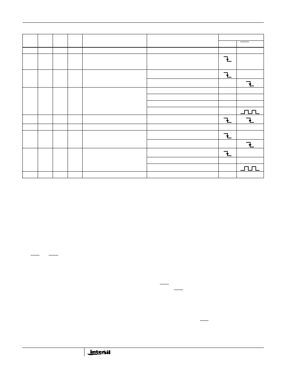
4-19
Digital Logic Inputs
Table 1 is the logic truth table for the 3V to 5V logic input
pins. A combination of the control pins C3, C2 and C1 select
1 of the possible 6 operating states. The 8th state listed is
Thermal Shutdown. Thermal Shutdown protection is invoked
if a fault condition on the tip or ring causes the junction
temperature of the die to exceed 175
o
C. A description of
each operating state and the control logic follows:
Open Circuit State (C3 = 0, C2 = 0, C1 = 0)
In this state, the tip and ring outputs are in a high impedance
condition (>1M
). No supervisory functions are available
and SHD and GKD outputs are at a TTL high level.
4-wire loopback testing can be performed in this state. With
the PTG pin floating, the signal on the V
TX
output is 180
o
out
of phase and approximately 2 times the V
RX
input signal. If
the PTG pin is grounded, then the amplitude will be
approximately the same as its input and 180
o
out of phase.
Ringing State (C3 = 0, C2 = 0, C1 = 1)
In this state, the output of the ring relay driver pin (RRLY)
goes low (energizing the ring relay to connect the ringing
signal to the phone) if either of the following two conditions
are satisfied:
(1) The RSYNC_REV pin is grounded through a resistor -
This connection enables the RRLY pin to go low the instant
the ringing state is invoked, without any regard for the ringing
voltage (90V
RMS
-120V
RMS
) across the relay contacts. The
resistor (34.8k
to 70k
) is required to limit the current into
the RSYNC_REV pin.
(2) A ring sync pulse is applied to the RSYNC_REV pin -
This connection enables the RRLY pin to go low at the
command of a ring sync pulse. A ring sync pulse should go
low at zero voltage crossing of the ring signal. This pulse
should have a rise and fall time <400
µ
s and a minimum
pulse width of 2ms.
Zero ring current detection is performed automatically
inside the SLIC. This feature de-energizes the ring relay
slightly before zero current occurs to partially compensate
for the delay in the opening of the relay.
The SHD output will go low when the subscriber goes off
hook. Once SHD is activated, an internal latch will prohibit
the re-ringing of the line until the ringing code is removed
and then reapplied.
The state prior to ringing the phone, can not be the Reverse
Active State. In the reverse active state the polarity of the
voltage on the CRT_REV_LVM capacitor, will make it appear
as if the subscriber is off hook. This subsequently will
activate an internal latch prohibiting the ringing of the line.
TABLE 1. DETECTOR STATES
STATE
C3
C2
C1
SLIC OPERATING STATE
ACTIVE DETECTOR
OUTPUT
SHD
GKD_ LVM
0
0
0
0
Open Circuit State
4 wire loopback test capability
HIGH
HIGH
1
0
0
1
Ringing State
(Previous State cannot be Reverse
Active State)
Ring Trip Detector
HIGH
2
0
1
0
Forward Active State
Loop Current Detector
Ground Key Detector
3
0
1
1
Test Active State
Requires previous state to be in the
Forward Active state to determine the
On hook or Off hook status of the line.
On Hook Loopback Detector
LOW
Ground Key Detector
HIGH
Off Hook Loop Current Detector
LOW
Line Voltage Detector
4
1
0
0
Tip Open - Ground Start State
Ground Key Detector
5
1
0
1
Reserved
Reserved
N/A
N/A
6
1
1
0
Reverse Active State
Loop Current Detector
Ground Key Detector
7
1
1
1
Test Reversal Active State
Requires previous state to be in the
Reverse Active state to determine the
On hook or Off hook status of the line.
On Hook Loop Current Detector
HIGH
Off Hook Loop Current Detector
LOW
Line Voltage Detector
8
X
X
X
Thermal Shutdown
LOW
LOW
HC55120, HC55121, HC55130, HC55131, HC55140, HC55141, HC55142, HC55143, HC55150, HC55151

4-20
The GKD_LVM output is disabled (TTL high level) during the
ringing state. Reference the Section titled "Ringing the
Phone" for more information.
Forward Active State (C3 = 0, C2 = 1, C1 = 0)
In this state, the SLIC is fully functional. The tip voltage is more
positive than the ring voltage. The tip and ring output voltages
are an unbalanced DC feed, reference Figure 13. Both SHD
and GKD supervisory functions are active. Reference the
section titled "DC Feed Curve" for more information.
Test Active State (C3 = 0, C2 = 1, C1 = 1)
Proper operation of the Test Active State requires the
previous state be the Forward Active state to determine the
on hook or off hook status of the line. In this state, the SLIC
can perform two different tests.
If the subscriber is on hook when the state is entered, a
loopback test is performed by switching an internal 600
resistor between tip and ring. The current flows through the
internal 600
is unidirectional via blocking diodes. (Cannot be
used in reverse.) When the loopback current flows, the SHD
output will go low and remain there until the state is exited. This
is intended to be a short test since the ability to detect
subscriber off hook is lost during loopback testing. Reference
the section titled "Loopback Tests" for more information.
If the subscriber is off hook when the state is entered, a Line
Voltage Measurement test is performed. The output of the
GKD_LVM pin is a pulse train. The pulse width of the active low
portion of the signal is proportional to the voltage across the tip
and ring pins. If the loop length is such that the SLIC is
operating in constant current, the tip to ring voltage can be used
to determine the length of the line under test. The longer the
line, the larger the tip to ring voltage and the wider the pulse.
This relationship can determine the length of the line for setting
gains in the system. Reference the section titled "Operation of
Line Voltage Measurement" for more information.
Tip Open State (C3 = 1, C2 = 0, C1 = 0)
In this state, the tip output is in a high impedance state
(>250k
)
and the ring output is capable of full operation, i.e.
has full longitudinal current capability. The Tip Open/Ground
Start state is used to interface to a PBX incoming 2-wire
trunk line. When a ground is applied through a resistor to the
ring lead, this current is detected and presented as a TTL
logic low on the SHD and GKD_LVM output pins.
Reserved (C3 = 1, C2 = 0, C1 = 1)
This state is undefined and reserved for future use.
Reverse Active State (C3 = 1, C2 = 1, C1 = 0)
In this state, the SLIC is fully functional. The ring voltage is
more positive than the tip voltage. The tip and ring output
voltages are an unbalanced DC feed, reference Figure 13.
The polarity reversal time is determined by the RC time
constant of the RSYNC_REV resistor and the
CRT_REV_LVM capacitor. Capacitor CRT_REV_LVM
performs three different functions: Ring trip filtering, polarity
reversal time and line voltage measurement. It is
recommended that programming of the reversal time be
accomplished by changing the value of RSYNC_REV resistor
(see Figure 18). The value of RSYNC_REV resistor is limited
between 34.8K (10ms) and 73.2k (21ms). Equation 39 gives
the formula for programming the reversal time.
Both SHD and GKD supervisory functions are active.
Reference the section titled "Polarity Reversal" for more
information.
Test Reversal Active State (C3 = 1, C2 = 1, C1 = 1)
Proper operation of the Test Reversal Active State requires
the previous state be the Reverse Active state to determine
the on hook or off hook status of the line.
If the subscriber is on hook when the state is entered, the
SLIC's tip and ring voltages are the same as the Reverse
Active state. The SHD output will go low when the subscriber
goes off hook and the GKD_LVM output is disabled (TTL
level high). (Note: operation is the same as the Reverse
Active state with the GKD_LVM output disabled.)
If the subscriber is off hook when the state is entered, a
Line Voltage Measurement test is performed.
The output of the GKD_LVM pin is a pulse train. The pulse width
of the active low portion of the signal is proportional to the voltage
across the tip and ring pins. If the loop length is such that the
SLIC is operating in constant current mode, the tip to ring voltage
can be used to determine the length of the line under test. The
longer the line, the larger the tip to ring voltage and the wider the
pulse. This relationship can determine the length of the line for
setting gains in the system. Reference the section titled
"Operation of Line Voltage Measurement" for more information.
Thermal Shutdown
The UniSLIC14's thermal shutdown protection is invoked if a
fault condition causes the junction temperature of the die to
exceed about 175
o
C. Once the thermal limit is exceeded,
both detector outputs go low (SHD and GKD_LVM) and one
of two things can happen.
For marginal faults where loop current is flowing during the
time of the over-temperature condition, foldback loop current
limiting reduces the loop current by reducing the tip to ring
voltage. An equilibrium condition will exist that maintains the
junction temperature at about 175
o
C until the fault condition
is removed.
For short circuit faults (tip or ring to ground, or to a supply,
etc.) that result in an over-temperature condition, the
foldback current limiting will try to maintain an equilibrium at
about 175
o
C. If the junction temperature keeps rising, the
device will thermally shutdown and disconnect tip and ring
until the junction temperature falls to approximately 150
o
C.
RSYNC
REV
≠
3.47k
ReversalTime ms
(
)
◊
=
(EQ. 39)
HC55120, HC55121, HC55130, HC55131, HC55140, HC55141, HC55142, HC55143, HC55150, HC55151
4-21
Supervisory Functions
Switch Hook Detect Threshold
The Switch Hook Detect Threshold is programmed with a
single external resistor (R
D
). The output of the SHD pin goes
low when an off hook condition is detected.
Ground Key Detect Threshold
The Ground Key Detect Threshold is set internally and is not
user programmable.
Ringing the Phone
The UniSLIC14 family handles all the popular ringing
formats with high or low side ring trip detection. High side
detection is possible because of the high common mode
range on the ring signal detect input pins (DT, DR). To
minimize power drain from the ring generator, when the
phone is not being rung, the sense resistors are typically
2M
. This reduces the current draw from the ring generator
to just a few microamps.
When the subscriber goes off hook during ringing, the
UniSLIC14 family automatically releases the ring relay and
DC feed is applied to the loop. The UniSLIC14 family has
very low power dissipation in the on hook active mode. This
enables the SLIC (during the ring cadence) to be powered
up in the active state, avoiding unnecessary powering up
and down of the SLIC. The control logic is designed to
facilitate easy implementation of the ring cadence, requiring
only one bit change to go from active to ringing and back
again.
DT, DR AND RRLY INPUTS
Ring trip detection will occur when the DR pin goes more
positive than DT by approximately 4V.
The ring relay driver pin, RRLY, has an internal clamp
between it's output and ground. This eliminates the need to
place an external snubber diode across the ring relay.
Reducing Impulse Noise During Ringing
With an increase in digital data lines being installed next to
analog lines, the threat from impulse noise on analog lines is
increasing. Impulse noise can cause large blocks of high
speed data to be lost, defeating most error correcting
techniques. The UniSLIC14 family has the capability to
reduce impulse noise by closing the ring relay at zero
voltage and opening the ring relay at zero current.
CLOSING THE RING RELAY AT ZERO VOLTAGE
Closing the ring relay at zero voltage is accomplished by
providing a ring sync pulse to the RSYNC_REV pin. The ring
sync pulse is synchronized to go low at the zero voltage
crossing of the ring signal. The resistor R1 in Figure 18 limits
the current into the RSYNC_REV pin. If a particular polarity
reversal time is required, then make R1 equal to the
calculated value in Equation 39. If a specific polarity reversal
time is not desired, R1 equal to 50k
is suggested.
The RSYNC_REV pin is designed to allow the ring sync
pulse to be present at all times. There is no need to gate the
ring sync pulse on and off. The logic control for the
RSYNC_REV pin cannot be an open collector. It must be
high (push-pull logic output stage / pull up resistor to VCC),
low or being clocked by the ring sync pulse. When the
RSYNC_REV pin is high the ring relay pin is disabled. When
the RSYNC_REV pin is low the ring relay pin is activated the
instant the logic code for ringing is applied.
OPENING THE RING RELAY AT ZERO CURRENT
The ring relay is automatically opened at zero current by the
SLIC. The SLIC logic requires zero ringing current in the
loop and either a valid switch hook detect (SHD) or a change
in the operating mode (cadence of the ringing signal) to
release the ring relay.
If the subscriber goes off hook during ringing, the SHD
output will go low. An internal latch will sense SHD is low and
disable the ring relay at zero ringing current. This prevents
the ring signal from being reapplied to the line. To ring the
line again, the SLIC must toggle between logic states. (Note:
The previous state can not be the Reverse Active State. In
the reverse state, the voltage on the CRT_REV_LVM
capacitor will activate an internal latch prohibiting the ringing
of the line.
Figure 19 shows the sequence of events from ringing the
phone to ring trip. The ring relay turns on when both the
ringing code and ring sync pulse are present (A). SHD is
high at this point. When the subscriber goes off hook the
SHD pin goes low and stays low until the ringing control
code is removed (B). This prevents the SHD output from
pulsing after ring trip occurs. At the next zero current
crossing of the ring signal, ring trip occurs and the ring relay
releases the line to allow loop current to flow in the loop (C).
FIGURE 18. REDUCING IMPULSE NOISE USING THE
RSYNC_REV PIN AND SETTING THE POLARITY
REVERSAL TIME
RSYNC_REV
24
R
1
INPUT FOR THE
RING SYNC PULSE
UniSLIC14
50k
5V
0V
HC55120, HC55121, HC55130, HC55131, HC55140, HC55141, HC55142, HC55143, HC55150, HC55151
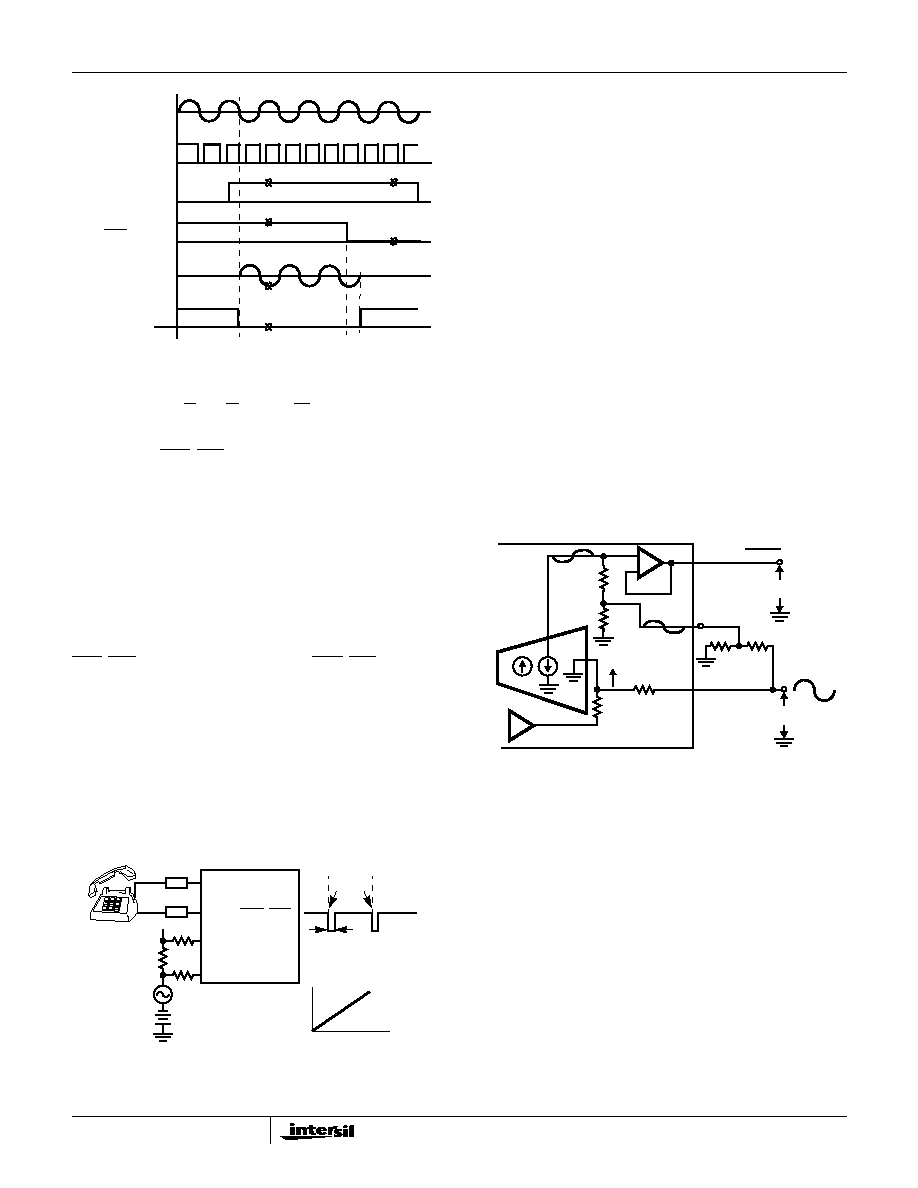
4-22
Operation of Line Voltage Measurement
A few of the SLICs in the UniSLIC14 family feature Line
Voltage Measurement (LVM) capability. This feature provides
a pulse on the GKD_LVM output pin that is proportional to
the loop voltage. Knowing the loop voltage and thus the loop
length, other basic cable characteristics such as attenuation
and capacitance can be inferred. Decisions can be made
about gain switching in the CODEC to overcome line losses
and verification of the 2-wire circuit integrity.
The LVM function can only be activated in the off hook
condition in either the forward or reverse operating states.
The LVM uses the ring signal supplied to the SLIC as a
timebase generator. The loop resistance is determined by
monitoring the pulse width of the output signal on the
GKD_LVM pin. The output signal on the GKD_LVM pin is a
square wave for which the average duration of the low state
is proportional to the average voltage between the tip and
ring terminals. The loop resistance is determined by the tip
to ring voltage and the constant loop current. Reference
Figure 20.
Although the logic state changes to the Test Active State
when performing this test, the SLIC is still powered up in the
active state (forward or reverse) and the subscriber is
unaware the measurement is being taken.
Polarity Reversal
Most of the SLICs in the UniSLIC14 family feature full
polarity reversal. Full polarity reversal means that the SLIC
can: transmit, determine the status of the line (on hook and
off hook) and provide "silent" polarity reversal. The value of
RSYNC_REV resistor is limited between 34.8k (10ms) and
73.2k (21ms). Reference Equation 39 to program the polarity
reversal time.
Transhybrid Balance
If a low cost CODEC is chosen that does not have a transmit
op-amp, the UniSLIC14 family of SLICs can solve this
problem without the need for an additional op-amp. The
solution is to use the Programmable Transmit Gain pin (PTG)
as an input for the receive signal (V
RX
). When the PTG pin is
connected to a divider network (R1 and R2 Figure 21) and the
value of R1 and R2 is much less than the internal 500k
resistors, two things happen. First the transmit gain from V
RX
to V
TX
is reduced by half. This is the result of shorting out the
bottom 500k
resistor with the much smaller external resistor.
And second, the input signal from V
RX
is also decreased in
half by resistors R1 and R2. Transhybrid balance occurs when
these two, equal but opposite in phase, signals are cancelled
at the input to the output buffer.
Loopback Tests
4-Wire Loopback Test
This feature can be very useful in the testing of line cards
during the manufacturing process and in field use. The test
is unobtrusive, allowing it to be used in live systems.
Reference Figure 22.
Most systems do not provide 4-wire loopback test
capability because of costly relays needed to switch in
external loads. All the SLICs in the UniSLIC14 family can
easily provide this function when configured in the Open
Circuit logic state. With the PTG pin floating, the signal on
the V
TX
output is 180
o
out of phase and approximately 2
times the V
RX
input signal. If the PTG pin is grounded, then
the amplitude will be approximately the same as the input
signal and 180
o
out of phase.
FIGURE 19. RINGING SEQUENCE
OFF
ON
OFF
RELAY DRIVER
RINGING CURRENT
IN LINE
SHD OUTPUT
RINGING CODE
APPLIED
RING SYNC
PULSE
RINGING VOLTAGE
(A)
(B)
(C)
FIGURE 20. OPERATION OF THE LINE VOLTAGE
MEASUREMENT CIRCUIT
TIP
RING
DT
DR
RING
GEN
GKD_LVM
RING
GEN
FREQ
PULSE WIDTH
PROPORTIONAL TO
LOOP LENGTH
PULSE
LOOP LENGTH
WIDTH
UniSLIC14
FIGURE 21. TRANSHYBRID BALANCE USING THE PTG PIN
V
TX
V
RX
V
TX
-
+
V
RX
+
-
500K
500K
500K
PTG
+
-
I
X
5
A = 1
I
X
R1
R2
500K
UniSLIC14
HC55120, HC55121, HC55130, HC55131, HC55140, HC55141, HC55142, HC55143, HC55150, HC55151
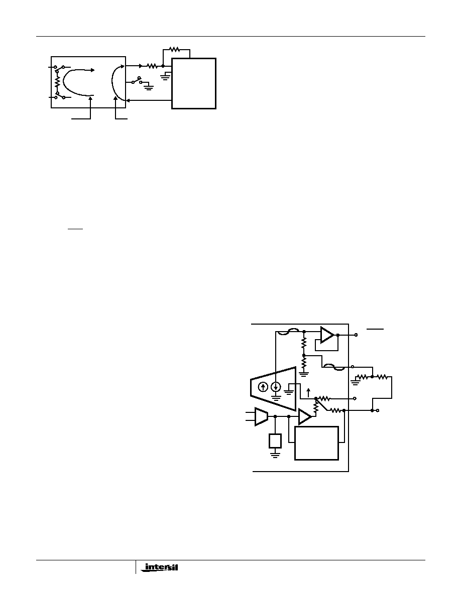
4-23
2-Wire Loopback Test
Most of the SLICs in the UniSLIC14 family feature 2-Wire
loopback testing. This loopback function is only activated
when the subscriber is on hook and the logic command to
the SLIC is in the Test Active State. (Note: if the subscriber is
off hook and in the Test Active State, the function performed
is the Line Voltage Measurement.)
During the 2-wire loopback test, a 2k
internal resistor is
switched across the tip and ring terminals of the SLIC. This
allows the SHD function and the 4-wire to 4-wire AC
transmission, right up to the subscriber loop, to be tested.
Together with the 4-wire loopback test in the Open Circuit
logic state, this 2-wire loopback test allows the complete
network (including SLIC) to be tested up to the subscriber
loop.
Pulse Metering
The HC55121, HC55142 and the HC55150 are designed to
support pulse metering. They offer solutions to the following
pulse metering design issues:
1) Providing adequate signal gain and current drive to the
subscriber metering equipment to overcome the attenuation
of this (12kHz, 16kHz) out of band signal.
2) Attenuating the pulse metering transhybrid signal without
severely attenuating the voice band signal to avoid clipping
in the CODEC/Filter.
3) Tailoring the overload levels in the SLIC to avoid clipping
of the combined voiceband and pulse metering signal.
4) Having the provision of silent polarity reversal as a backup
in the case where the loop attenuates the out of band signal
too much for it to be detected by the subscriber's metering
equipment.
Adequate Signal Gain
Adequate signal gain and current drive to the subscriber's
metering equipment is made easier by the network shown in
Figure 23. The pulse metering signal is supplied to a
dedicated high impedance input pin called SPM. The circuit
in Figure 23 shows the connection of a network that sets the
2-wire impedance (Z
TR
), at the pulse metering frequencies,
to be approximately 200
. If the line impedance (Z
L
) is equal
to 200
at the pulse metering frequencies, then the 4-Wire
to 2-wire gain (V
TR
/ SPM) is equal 4. Thereby lowering the
input signal requirements of the pulse metering signal.
Note: The automatic pulse metering 2-wire impedance
matching is independent of the programmed 2-wire
impedance matching at voiceband frequencies.
Calculation of the pulse metering gain is achieved by
replacing V
RX
/500k in Equation 15 with SPM/125k and
following the same process through to Equation 21. The
UniSLIC14 sets the 2-wire input impedance of the SLIC
(Z
TR
), including the protection resistors, equal to 200
. The
results are shown in Equation 40.
Avoiding Clipping in the CODEC/Filter
The amplitude of the returning pulse metering signal is often
very large and could easily over drive the input to the
CODEC/Filter. By using the same method discussed in
section "Transhybrid Balance", most if not all of the pulse
metering signal can be canceled out before it reaches the
input to the CODEC/Filter. This connection is shown in
Figure 23.
Overload Levels and Silent Polarity Reversal
The pulse metering signal and voice are simultaneously
transmitted, and therefore require additional overhead to
prevent distortion of the signal. Reference section "Off hook
Overhead Voltage" to account for the additional pulse
metering signal requirements.
Most of the SLICs in the UniSLIC14 family feature full
polarity reversal. Full polarity reversal means that the SLIC
can: transmit, determine the status of the line (on hook and
off hook) and provide "silent" polarity reversal. Reference
Equation 39 to program the polarity reversal time.
FIGURE 22. 4-WIRE AND 2-WIRE LOOPBACK TESTS
V
TX
V
RX
TIP
RING
4-WIRE LOOPBACK
UniSLIC14
600
DUAL SUPPLY
CODEC/FILTER
INTERNAL
2-WIRE LOOPBACK
+
-
PTG
A
4-2
=
V
TR
SPM
-------------
= 8
≠
Z
L
Z
L
+ Z
TR
-------------------------
8
200
200 + 200
---------------------------
≠
4
≠
=
=
(EQ. 40)
FIGURE 23. PULSE METERING WITH TRANSHYBRID
BALANCE
V
TX
V
RX
= 0
500K
500K
500K
PTG
+
-
I
X
A = 1
I
X
R1
R2
500K
UniSLIC14
Z
T
1/80K
5
125K
SPM
12/16kHz
PULSE METERING
INPUT SIGNAL
SETS 2-WIRE
IMPEDANCE
AT 12-16kHz
EQUAL TO
200
HC55120, HC55121, HC55130, HC55131, HC55140, HC55141, HC55142, HC55143, HC55150, HC55151
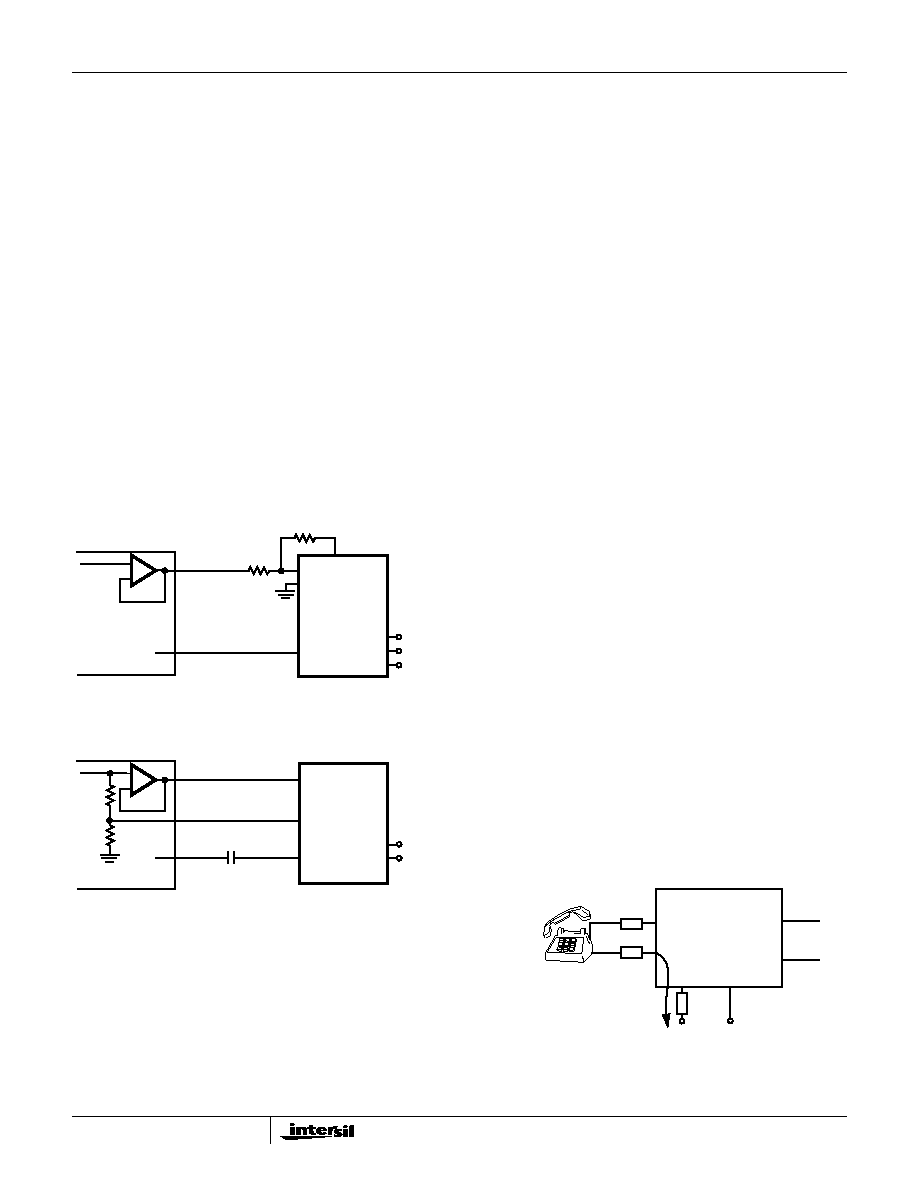
4-24
Interface to Dual and Single Supply
CODECs
Great care has been taken to minimize the number of external
components required with the UniSLIC14 family while still
providing the maximum flexibility. Figures 24A, 24B) shows
the connection of the UniSLIC14 to both a dual supply
CODEC/Filter and a single supply DSP CODEC/Filter.
To eliminate the DC blocking capacitors between the SLIC
and the CODEC/Filter when using a dual supply
CODEC/Filter, both the receive and transmit leads of the
SLIC are referenced to ground. This leads to a very simple
SLIC to CODEC/Filter interface, as shown in Figure 24A.
When using a single supply DSP CODEC/Filter the output
and input of the CODEC/Filter are no longer referenced to
ground. To achieve maximum voltage swing with a single
supply, both the output and input of the CODEC/Filter are
referenced to its own V
CC
/2 reference. Thus, DC blocking
capacitors are once again required. By using the PTG pin of
the UniSLIC14 and the externally supplied V
CC
/2 reference
of the CODEC/Filter, one of the DC blocking capacitors can
be eliminated (Figure 24B).
Power Management
The UniSLIC14 family provides two distinct power
management capabilities:
Power Sharing and Battery Selection
Power Sharing
Power sharing is a method of redistributing the power away
from the SLIC in short loop applications. The total system
power is the same, but the die temperature of the SLIC is
much lower. Power sharing becomes important if the
application has a single battery supply (-48V on hook
requirements for faxes and modems) and the possibility of
high loop currents (reference Figure 25). This technique
would prevent the SLIC from getting too hot and thermally
shutting down on short loops.
The power dissipation in the SLIC is the sum of the smaller
quiescent supply power and the much larger power that
results from the loop current. The power that results from the
loop current is the loop current times the voltage across the
SLIC. The power sharing resistor (R
PS
) reduces the voltage
across the SLIC, and thereby the on-chip power dissipation.
The voltage across the SLIC is reduced by the voltage drop
across R
PS
. This occurs because R
PS
is in series with the
loop current and the negative supply.
A mathematical verification follows:
Given: V
BH
= V
BL
= -48V, Loop current = 30mA, R
L
(load
across tip and ring) = 600
, Quiescent battery power =
(48V) (0.8mA) = 38.4mW, Quiescent VCC power = (5V)
(2.7mA) = 13.5mW, Power sharing resistor = 600
.
1. Without power sharing, the on-chip power dissipation
would be 952mW (Equation 41).
2. With power sharing, the on-chip power dissipation is
412mW (Equation 42). A power redistribution of 540mW.
On-chip power dissipation without power sharing resistor.
On-chip power dissipation with 600
power sharing resistor.
The design trade-off in using the power sharing resistor is
loop length vs on-chip power dissipation.
FIGURE 24A.
FIGURE 24B.
FIGURE 24. INTERFACE TO DUAL AND SINGLE SUPPLY
CODECs
V
TX
+
-
A = 1
V
RX
UniSLIC14
V
OUT
DUAL SUPPLY
CODEC/FILTER
+
-
5V
GND
-5V
V
TX
500K
PTG
+
-
A = 1
500K
V
RX
UniSLIC14
SINGLE SUPPLY
CODEC/FILTER
5V
GND
DSP
V
IN
V
OUT
V
REF
PD
V
BH
(
)
30mA
(
)
38.4mW
13.5mW
RL
(
)
30mA
(
)
2
≠
+
+
=
(EQ. 41)
PD
952mW
=
PD
V
BH
(
)
30mA
(
)
38.4mW
13.5mW
+
+
=
(EQ. 42)
R
L
(
)
30mA
(
)
2
≠
R
PS
(
)
30mA
(
)
2
≠
PD
412mW
=
FIGURE 25. POWER SHARING (SINGLE SUPPLY SYSTEMS)
V
TX
V
RX
UniSLIC14
TIP
RING
V
BL
V
BH
-48V
-48V
ON SHORT LOOPS, THE
MAJORITY OF CURRENT
FLOWS OUT THE V
BL
PIN
R
PS
HC55120, HC55121, HC55130, HC55131, HC55140, HC55141, HC55142, HC55143, HC55150, HC55151
4-25
Battery Selection
Battery selection is a technique, for a two battery supply
system, where the SLIC automatically diverts the loop
current to the most appropriate supply for a given loop
length. This results in significant power savings and lowers
the total power consumption on short loops. This technique
is particularly useful if most of the lines are short, and the on
hook condition requires a -48V battery. In Figure 26, it can
be seen that for long loops the majority of the current comes
from the high battery supply (V
BH
) and for short loops from
the low battery supply (V
BL
).
FIGURE 26. BATTERY SELECTION (DUAL SUPPLY SYSTEMS)
LOOP CURRENT (mA)
0
35
30
25
20
15
10
5
1000
900
800
600
700
575
550
525
500
475
450
400
350
300
250
200
150
2000
LOOP RESISTANCE (
)
100
40
VBH = -48V
VBL = -24V
RILim = 33.2k
V
BL
V
BH
V
BH
V
BL
Pinouts - 28 Lead PLCC Packages
HC55120
(28 LEAD PLCC)
TOP VIEW
HC55121
(28 LEAD PLCC)
TOP VIEW
HC55130
(28 LEAD PLCC)
TOP VIEW
HC55140
(28 LEAD PLCC)
TOP VIEW
DR
C3
C2
C1
SHD
CDC
DT
RRL
Y
PTG
VTX
NC
VRX
ZT
CH
RSYNC
ILIM
ROH
RD
AGND
GKD
V
CC
1
2
3
4
5
6
7
8
9
10
11
12
13
14
15
16
17
18
19
20
21
22
23
24
25
26
27
28
BGND
TIP
VBH
VBL
RING
CRT
RDC_RAC
DR
C3
C2
C1
SHD
CDC
DT
RRL
Y
PTG
VTX
SPM
VRX
ZT
CH
RSYNC_REV
ILIM
ROH
RD
AGND
GKD
V
CC
1
2
3
4
5
6
7
8
9
10
11
12
13
14
15
16
17
18
19
20
21
22
23
24
25
26
27
28
BGND
TIP
VBH
VBL
RING
CRT_REV
RDC_RAC
DR
C3
C2
C1
SHD
CDC
DT
RRL
Y
PTG
VTX
NC
VRX
ZT
CH
RSYNC
ILIM
ROH
RD
AGND
NC
V
CC
1
2
3
4
5
6
7
8
9
10
11
12
13
14
15
16
17
18
19
20
21
22
23
24
25
26
27
28
BGND
TIP
VBH
VBL
RING
CRT
RDC_RAC
DR
C3
C2
C1
SHD
CDC
DT
RRL
Y
PTG
VTX
NC
VRX
ZT
CH
RSYNC_REV
ILIM
ROH
RD
AGND
GKD_LVM
V
CC
1
2
3
4
5
6
7
8
9
10
11
12
13
14
15
16
17
18
19
20
21
22
23
24
25
26
27
28
BGND
TIP
VBH
VBL
RING
CRT_REV_
RDC_RAC
LVM
HC55120, HC55121, HC55130, HC55131, HC55140, HC55141, HC55142, HC55143, HC55150, HC55151
4-26
HC55142
(28 LEAD PLCC)
TOP VIEW
HC55150
(28 LEAD PLCC)
TOP VIEW
Pinouts - 32 Lead PLCC Packages
HC55120
(32 LEAD PLCC)
TOP VIEW
HC55121
(32 LEAD PLCC)
TOP VIEW
Pinouts - 28 Lead PLCC Packages
(Continued)
DR
C3
C2
C1
SHD
CDC
DT
RRL
Y
PTG
VTX
SPM
VRX
ZT
CH
RSYNC_REV
ILIM
ROH
RD
AGND
GKD_LVM
V
CC
1
2
3
4
5
6
7
8
9
10
11
12
13
14
15
16
17
18
19
20
21
22
23
24
25
26
27
28
BGND
TIP
VBH
VBL
RING
CRT_REV_
RDC_RAC
LVM
DR
C3
C2
C1
SHD
CDC
DT
RRL
Y
PTG
VTX
SPM
VRX
ZT
CH
RSYNC_REV
ILIM
ROH
RD
AGND
LVM
V
CC
1
2
3
4
5
6
7
8
9
10
11
12
13
14
15
16
17
18
19
20
21
22
23
24
25
26
27
28
BGND
TIP
VBH
VBL
RING
CRT_REV_
RDC_RAC
LVM
DR
C3
C2
C1
SHD
CDC
DT
RRL
Y
PTG
VTX
VRX
ZT
CH
RSYNC
ILIM
ROH
RD
AGND
GKD
V
CC
1
2
3
4
5
6
7
8
9
10
11
14
15
16
17
18
19
20
30
31
32
BGND
TIP
VBH
VBL
RING
CRT
RDC_RAC
12
13
C5
C4
29
28
27
26
25
24
23
22
21
NC
TRL
Y2
TRL
Y1
DR
C3
C2
C1
SHD
CDC
DT
RRL
Y
PTG
VTX
VRX
ZT
CH
RSYNC_REV
ILIM
ROH
RD
AGND
GKD
V
CC
1
2
3
4
5
6
7
8
9
10
11
14
15
16
17
18
19
20
30
31
32
BGND
TIP
VBH
VBL
RING
CRT_REV
RDC_RAC
12
13
C5
C4
29
28
27
26
25
24
23
22
21
NC
TRL
Y2
TRL
Y1
HC55120, HC55121, HC55130, HC55131, HC55140, HC55141, HC55142, HC55143, HC55150, HC55151
4-27
HC55130
(32 LEAD PLCC)
TOP VIEW
HC55140
(32 LEAD PLCC)
TOP VIEW
HC55142
(32 LEAD PLCC)
TOP VIEW
HC55150
(32 LEAD PLCC)
TOP VIEW
Pinouts - 32 Lead PLCC Packages
DR
C3
C2
C1
SHD
CDC
DT
RRL
Y
PTG
VTX
VRX
ZT
CH
RSYNC
ILIM
ROH
RD
AGND
NC
V
CC
1
2
3
4
5
6
7
8
9
10
11
14
15
16
17
18
19
20
30
31
32
BGND
TIP
VBH
VBL
RING
CRT
RDC_RAC
12
13
C5
C4
29
28
27
26
25
24
23
22
21
NC
TRL
Y2
TRL
Y1
DR
C3
C2
C1
SHD
CDC
DT
RRL
Y
PTG
VTX
VRX
ZT
CH
RSYNC_REV
ILIM
ROH
RD
AGND
GKD_LVM
V
CC
1
2
3
4
5
6
7
8
9
10
11
14
15
16
17
18
19
20
30
31
32
BGND
TIP
VBH
VBL
RING
CRT_REV_LVM
RDC_RAC
12
13
C5
C4
29
28
27
26
25
24
23
22
21
NC
TRL
Y2
TRL
Y1
DR
C3
C2
C1
SHD
CDC
DT
RRL
Y
PTG
VTX
VRX
ZT
CH
RSYNC_REV
ILIM
ROH
RD
AGND
GKD_LVM
V
CC
1
2
3
4
5
6
7
8
9
10
11
14
15
16
17
18
19
20
30
31
32
BGND
TIP
VBH
VBL
RING
CRT_REV_
RDC_RAC
12
13
C5
C4
29
28
27
26
25
24
23
22
21
SPM
TRL
Y2
TRL
Y1
LVM
DR
C3
C2
C1
SHD
CDC
DT
RRL
Y
PTG
VTX
VRX
ZT
CH
RSYNC_REV
ILIM
ROH
RD
AGND
LVM
V
CC
1
2
3
4
5
6
7
8
9
10
11
14
15
16
17
18
19
20
30
31
32
BGND
TIP
VBH
VBL
RING
CRT_REV_
RDC_RAC
12
13
C5
C4
29
28
27
26
25
24
23
22
21
SPM
TRL
Y2
TRL
Y1
LVM
HC55120, HC55121, HC55130, HC55131, HC55140, HC55141, HC55142, HC55143, HC55150, HC55151
4-28
Pinouts - 28 Lead SOIC Packages
HC55120
(28 LEAD SOIC)
TOP VIEW
HC55121
(28 LEAD SOIC)
TOP VIEW
HC55130
(28 LEAD SOIC)
TOP VIEW
HC55140
(28 LEAD SOIC)
TOP VIEW
ZT
PTG
RRLY
CH
RING
BGND
TIP
VBH
VBL
RDC_RAC
CDC
DT
DR
CRT
AGND
NC
VRX
RSYNC
ILIM
RD
SHD
C1
C2
C3
GKD
VTX
ROH
V
CC
28
27
26
25
24
23
22
21
20
19
18
17
16
15
1
2
3
4
5
6
7
8
9
10
11
12
13
14
ZT
PTG
RRLY
CH
RING
BGND
TIP
VBH
VBL
RDC_RAC
CDC
DT
DR
CRT_REV
AGND
SPM
VRX
RSYNC_REV
ILIM
RD
SHD
C1
C2
C3
GKD
VTX
ROH
V
CC
28
27
26
25
24
23
22
21
20
19
18
17
16
15
1
2
3
4
5
6
7
8
9
10
11
12
13
14
ZT
PTG
RRLY
CH
RING
BGND
TIP
VBH
VBL
RDC_RAC
CDC
DT
DR
CRT
AGND
NC
VRX
RSYNC
ILIM
RD
SHD
C1
C2
C3
NC
VTX
ROH
V
CC
28
27
26
25
24
23
22
21
20
19
18
17
16
15
1
2
3
4
5
6
7
8
9
10
11
12
13
14
ZT
PTG
RRLY
CH
RING
BGND
TIP
VBH
VBL
RDC_RAC
CDC
DT
DR
CRT_REV_LVM
AGND
NC
VRX
RSYNC_REV
ILIM
RD
SHD
C1
C2
C3
GKD_LVM
VTX
ROH
V
CC
28
27
26
25
24
23
22
21
20
19
18
17
16
15
1
2
3
4
5
6
7
8
9
10
11
12
13
14
HC55120, HC55121, HC55130, HC55131, HC55140, HC55141, HC55142, HC55143, HC55150, HC55151
4-29
HC55142
(28 LEAD SOIC)
TOP VIEW
HC55150
(28 LEAD SOIC)
TOP VIEW
Pinouts - 28 Lead SOIC Packages
(Continued)
ZT
PTG
RRLY
CH
RING
BGND
TIP
VBH
VBL
RDC_RAC
CDC
DT
DR
CRT_REV_LVM
AGND
SPM
VRX
RSYNC_REV
ILIM
RD
SHD
C1
C2
C3
GKD_LVM
VTX
ROH
V
CC
28
27
26
25
24
23
22
21
20
19
18
17
16
15
1
2
3
4
5
6
7
8
9
10
11
12
13
14
ZT
PTG
RRLY
CH
RING
BGND
TIP
VBH
VBL
RDC_RAC
CDC
DT
DR
CRT_REV_LVM
AGND
SPM
VRX
RSYNC_REV
ILIM
RD
SHD
C1
C2
C3
LVM
VTX
ROH
V
CC
28
27
26
25
24
23
22
21
20
19
18
17
16
15
1
2
3
4
5
6
7
8
9
10
11
12
13
14
Pin Descriptions
28
PIN
PLCC
32
PIN
PLCC
28
PIN
SOIC
SYMBOL
DESCRIPTION
1
1
2
PTG
Programmable Transmit Gain - The 2-wire to 4-wire transmission gain is 0dB if this pin is left floating
and -6.02dB if tied to ground. The -6.02dB gain option is useful in systems where Pulse Metering is
used. See Figure 23.
2
2
3
RRLY
Ring Relay Driver Output - The relay coil may be connected to a maximum of 14V.
3
3
4
CH
AC/DC Separation Capacitor - CH is required to properly process the AC current from the DC loop
current. Recommended value 0.1
µ
F.
4
4
1
ZT
2-Wire Impedance Matching Pin - Impedance matching of the 2-wire side is accomplished by placing
an impedance between the ZT pin and ground. See Equation 32.
5
5
5
RING
Connects via protection resistor R
P
to ring wire of subscriber pair.
6
6
6
BGND
Battery ground.
7
7
7
TIP
Connects via protection resistor R
P
to tip wire of subscriber pair.
8
8
8
V
BH
High Battery Supply (negative with respect to GND).
9
9
9
V
BL
Low Battery Supply (negative with respect to GND, magnitude
V
BH
).
10
10
10
RDC_RAC
Resistive Feed/Anti Clipping - Performs anti clipping function on constant current application and sets
the slope of the resistive feed curve for constant voltage applications.
11
11
14
CRT_REV
_LVM
Ring Trip, Soft Polarity Reversal and Line Voltage Measurement - A capacitor when placed between the
CRT_REV_LVM pin and +5V performs 3 mutually exclusive functions. When the SLIC is configured in the
Ringing mode it provides filtering of the ringing signal to prevent false detect. When the SLIC is transitioning
between the Forward Active State and Reverse Active State it provides Soft Polarity Reversal and performs
charge storage in the Line Voltage Measurement State. Recommended value 0.47
µ
F.
12
12
11
CDC
Filter Capacitor- The CDC Capacitor removes the VF signals from the battery feed control loop.
13
13
12
DT
Tip side of Ring Trip Detector - Ring trip detection is accomplished by connecting an external network
to a detector in the SLIC with inputs DT and DR. Ring trip occurs when the voltage on DT is more
negative than the voltage on DR.
14
14
13
DR
Ring Side of Ring Trip Detector - Ring trip detection is accomplished by connecting an external
network to a detector in the SLIC with inputs DT and DR. Ring trip occurs when the voltage on DR is
more positive than the voltage on DT.
-
15
-
C5
Activates Test Relay TRLY2.
HC55120, HC55121, HC55130, HC55131, HC55140, HC55141, HC55142, HC55143, HC55150, HC55151

4-30
-
16
-
C4
Activates Test Relay TRLY1.
15
17
16
C3
TTL Compatible Logic Input. The logic states of C1, C2 and C3 determine the operating states of the
SLIC. Reference Table 1 for details.
16
18
17
C2
TTL Compatible Logic Input. The logic states of C1, C2 and C3 determine the operating states of the
SLIC. Reference Table 1 for details.
17
19
18
C1
TTL Compatible Logic Input. The logic states of C1, C2 and C3 determine the operating states of the
SLIC. Reference Table 1 for details.
18
20
19
SHD
Switch Hook Detect - Active during off hook, ground key and loopback. Reference Table 1 for details.
19
21
15
GKD_LVM
Ground Key Detector and Line Voltage Measurement - Reference Table 1 for details.
20
22
20
V
CC
5V Supply.
21
23
21
RD
Loop Current Threshold Programming Pin - A resistor between this pin and ground will determine the
trigger level for the loop current detect circuit. See Equation 7.
22
24
22
ROH
Off Hook Overload Setting Resistor - Used to set combined overhead for voice and pulse metering
signals. See Equation 10.
23
25
23
ILIM
Current Limit Programming Pin - A resistor between this pin and ground will determine the constant
current limit of the feed curve. See Equation 11.
24
26
24
RSYNC_REV
Ring Synchronization Input and Reversal Time Setting. A resistor between this pin and GND
determines the polarity reversal time. Synchronization of the closing of the relay at zero voltage is
achieved via a ring sync pulse (5V to 0V) synchronized to the ring signal zero voltage crossing
(Reference Figure 18).
25
27
28
AGND
Analog ground
26
28
25
VRX
Receive Input - Ground referenced 4-wire side.
27
29
26
SPM
Pulse Metering Signal Input. If pulse metering is not used, then this pin should be grounded as close
to the device pin as possible.
28
30
27
VTX
Transmit Output - Ground referenced 4-wire side.
-
31
-
TRLY2
Test Relay Driver 2.
-
32
-
TRLY1
Test Relay Driver 1.
Pin Descriptions
(Continued)
28
PIN
PLCC
32
PIN
PLCC
28
PIN
SOIC
SYMBOL
DESCRIPTION
HC55120, HC55121, HC55130, HC55131, HC55140, HC55141, HC55142, HC55143, HC55150, HC55151

4-31
Basic Application Circuit
Voice Only 28 Lead PLCC Package
TIP
RING
FIGURE 27. UniSLIC14 VOICE ONLY BASIC APPLICATION CIRCUIT
V
TX
V
RX
ZT
RSYNC_REV
ILIM
ROH
RD
SHD
GKD_LVM
C1
C2
C3
V
CC
RRLY
CH
BGND
VBH
VBL
RDC_RAC
CDC
DR
DT
CRT_REV_LVM
C
1
+5V
+5V OR
RELAY
C
2
-24V
C
5
-48V
R
1
C
3
R
P
RING
TIP
R
P
R
2
R
3
VBAT
RING
CONTROL LOGIC
R
4
R
6
R
7
R
8
R
5
R
9
R
10
R
11
CODEC/FILTER
C
4
R
12
U1
U2
1
2
3
4
5
6
7
8
9
10
11
12
13
14
15
16
17
18
19
20
21
22
23
24
26
28
PTG
GENERATOR
C7
+5V
C
6
AGND
25
C
8
C
9
SPM
27
+12V
D
1
OPTIONAL
PERFORM TRANSHYBRID BALANCE
WHEN USING A NON-DSP CODEC.
NOT REQUIRED FOR
C10
C11
NON-DSP CODEC's.
NOT REQUIRED FOR DSP CODEC.
REQUIRED FOR DSP CODEC's
TABLE 2. BASIC APPLICATION CIRCUIT COMPONENT LIST
COMPONENT
VALUE
TOLERANCE
RATING
U1 - SLIC
UniSLIC14 Family
N/A
N/A
U2 - Dual Asymmetrical Transient Voltage Suppressor
TISP1072F3
N/A
N/A
RP (Line Feed Resistors)
30
Matched 1%
2.0W
R1 (RDC_RAC Resistor)
21k
1%
1/16W
R2, R3
2M
1%
1/16W
R4 (RD Resistor)
41.2k
1%
1/16W
R5 (ROH Resistor)
38.3k
1%
1/16W
R6 (RILIM Resistor)
33.2k
1%
1/16W
R7 (RSYNC_REV Resistor)
34.8k
1%
1/16W
R8 (RZT Resistor)
107k
1%
1/16W
R9, R10, R11
20k
1%
1/16W
R12
400
5%
2W
C1 (Supply Decoupling), C2
0.1
µ
F
20%
10V
C5 (Supply Decoupling)
0.1
µ
F
20%
50V
C6 (Supply Decoupling)
0.1
µ
F
20%
100V
C4, C7, C10, C11
0.47
µ
F
20%
10V
C3
4.7
µ
F
20%
50V
C8, C9
2200pF
20%
100V
D1, Recommended if the VBL supply is not derived from the VBH Supply
1N4004
-
-
Design Parameters: Maximum on hook voltage = 0.775V
RMS
, Maximum Off hook Voice = 3.2V
PEAK
, Switch Hook Threshold = 12mA, Loop
Current Limit = 31mA, Synthesize Device Impedance = 540
(600 - 60), with 30
protection resistors, impedance across Tip and Ring terminals =
600
. Where applicable, these component values apply to the Basic Application Circuits for the HC55120, HC55121, HC55130/1, HC55140/1,
HC55142/3 and HC55150/1. Pins not shown in the Basic Application Circuit are no connect (NC) pins.
HC55120, HC55121, HC55130, HC55131, HC55140, HC55141, HC55142, HC55143, HC55150, HC55151
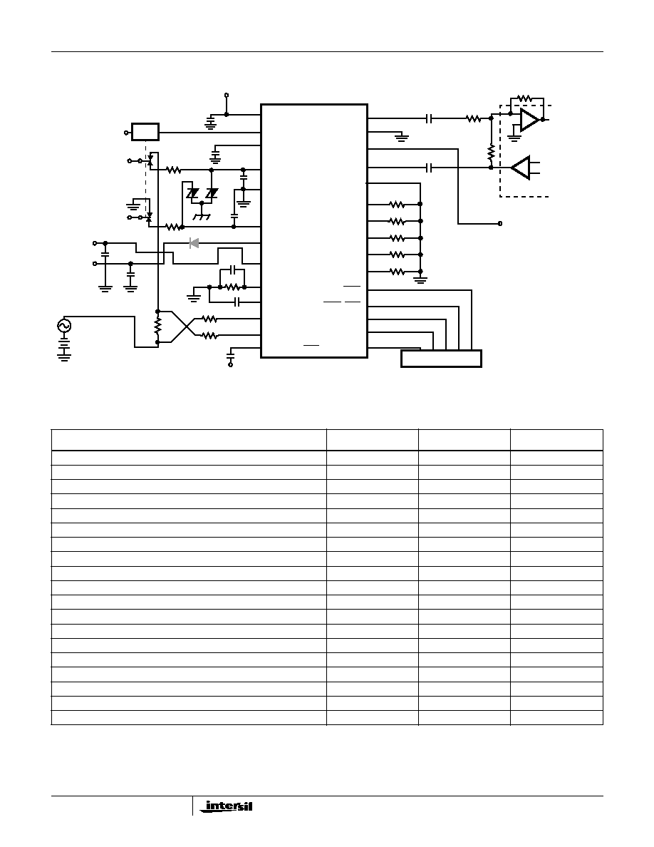
4-32
Basic Application Circuit
Pulse Metering 28 Lead PLCC Package
FIGURE 28. UniSLIC14 PULSE METERING BASIC APPLICATION CIRCUIT
V
TX
VRX
ZT
RSYNC_REV
ILIM
R
OH
RD
SHD
GKD_LVM
C1
C2
C3
V
CC
RRLY
CH
VBH
VBL
RDC_RAC
CDC
DR
DT
CRT_REV_LVM
C
1
+5V
RELAY
C
2
C
3
R
P
RING
TIP
R
P
R
2
R
3
V
BAT
RING
CONTROL LOGIC
R
4
R
6
R
7
R
8
R
5
R
9
R
10
R
11
CODEC/FILTER
C
4
R
12
U1
2
3
8
9
11
12
13
14
20
1
4
15
16
17
18
19
21
22
23
24
26
28
PTG
AGND
SPM
12/16kHz
PULSE METERING
INPUT SIGNAL
GENERATOR
R
1
10
C7
+5V
-24V
C
5
-48V
C
6
25
27
TIP
RING
BGND
U2
5
6
7
C
8
C
9
+5V OR
+12V
D
1
OPTIONAL
C10
C11
PERFORM TRANSHYBRID BALANCE
WHEN USING A NON-DSP CODEC.
NOT REQUIRED FOR
NON-DSP CODEC's.
NOT REQUIRED FOR DSP CODEC.
REQUIRED FOR DSP CODEC's
TABLE 3. BASIC APPLICATION CIRCUIT COMPONENT LIST
COMPONENT
VALUE
TOLERANCE
RATING
U1 - SLIC
UniSLIC14 Family
N/A
N/A
U2 - Dual Asymmetrical Transient Voltage Suppressor
TISP1072F3
N/A
N/A
RP (Line Feed Resistors)
30
Matched 1%
2.0W
R1 (RDC_RAC Resistor)
26.1k
1%
1/16W
R2, R3
2M
1%
1/16W
R4 (RD Resistor)
41.2k
1%
1/16W
R5 (ROH Resistor)
38.3k
1%
1/16W
R6 (RILIM Resistor)
33.2k
1%
1/16W
R7 (RSYNC_REV Resistor)
34.8k
1%
1/16W
R8 (RZT Resistor)
107k
1%
1/16W
R9, R10, R11
20k
1%
1/16W
R12
400
5%
2W
C1 (Supply Decoupling), C2
0.1
µ
F
20%
10V
C5 (Supply Decoupling)
0.1
µ
F
20%
50V
C6 (Supply Decoupling)
0.1
µ
F
20%
100V
C4, C7, C10, C11
0.47
µ
F
20%
10V
C3
4.7
µ
F
20%
50V
C8, C9
2200pF
20%
100V
D1, Recommended if the VBL supply is not derived from the VBH Supply
1N4004
-
-
Design Parameters: Maximum on hook voltage = 0.775V
RMS
, Maximum off hook voice = 1.1V
PEAK
, Maximum simultaneous pulse metering
signal = 2.2V
RMS
, Switch Hook Threshold = 12mA, Loop Current Limit = 31mA, Synthesize Device Impedance = 540
(600 - 60), with 30
protection resistors, impedance across Tip and Ring terminals = 600
. Where applicable, these component values apply to the Basic Application
Circuits for the HC55120, HC55121, HC55130/1, HC55140/1, HC55142/3 and HC55150/1. Pins not shown in the Basic Application Circuit are
no connect (NC) pins.
HC55120, HC55121, HC55130, HC55131, HC55140, HC55141, HC55142, HC55143, HC55150, HC55151

4-33
Basic Application Circuit
Voice Only 28 Lead SOIC Package
FIGURE 29. UniSLIC14 VOICE ONLY BASIC APPLICATION CIRCUIT
V
TX
V
RX
ZT
RSYNC_REV
ILIM
R
OH
RD
SHD
GKD_LVM
C1
C2
C3
V
CC
RRLY
CH
V
BH
V
BL
RDC_RAC
CDC
DR
DT
CRT_REV_LVM
C
1
+5V
RELAY
C
2
R
1
C
3
R
P
RING
TIP
R
P
R
2
R
3
V
BAT
RING
CONTROL LOGIC
R
4
R
6
R
7
R
8
R
5
R
9
R
10
R
11
CODEC/FILTER
C
4
R
12
U1
1
3
4
8
9
10
11
12
13
14
15
16
17
18
19
20
21
22
23
24
25
27
GENERATOR
C7
+5V
-24V
C
5
-48V
C
6
AGND
28
TIP
RING
BGND
U2
5
6
7
C
8
C
9
SPM
26
+5V OR
+12V
D
1
OPTIONAL
C10
C11
PERFORM TRANSHYBRID BALANCE
WHEN USING A NON-DSP CODEC.
NOT REQUIRED FOR
NON-DSP CODEC's.
NOT REQUIRED FOR DSP CODEC.
REQUIRED FOR DSP CODEC's
TABLE 4. BASIC APPLICATION CIRCUIT COMPONENT LIST
COMPONENT
VALUE
TOLERANCE
RATING
U1 - SLIC
UniSLIC14 Family
N/A
N/A
U2 - Dual Asymmetrical Transient Voltage Suppressor
TISP1072F3
N/A
N/A
RP (Line Feed Resistors)
30
Matched 1%
2.0W
R1 (RDC_RAC Resistor)
21k
1%
1/16W
R2, R3
2M
1%
1/16W
R4 (RD Resistor)
41.2k
1%
1/16W
R5 (ROH Resistor)
38.3k
1%
1/16W
R6 (RILIM Resistor)
33.2k
1%
1/16W
R7 (RSYNC_REV Resistor)
34.8k
1%
1/16W
R8 (RZT Resistor)
107k
1%
1/16W
R9, R10, R11
20k
1%
1/16W
R12
400
5%
2W
C1 (Supply Decoupling), C2
0.1
µ
F
20%
10V
C5 (Supply Decoupling)
0.1
µ
F
20%
50V
C6 (Supply Decoupling)
0.1
µ
F
20%
100V
C4, C7, C10, C11
0.47
µ
F
20%
10V
C3
4.7
µ
F
20%
50V
C8, C9
2200pF
20%
100V
D1, Recommended if the VBL supply is not derived from the VBH Supply
1N4004
-
-
Design Parameters: Maximum on hook voltage = 0.775V
RMS
, Maximum Off hook Voice = 3.2V
PEAK
, Switch Hook Threshold = 12mA, Loop
Current Limit = 31mA, Synthesize Device Impedance = 540
(600 - 60), with 30
protection resistors, impedance across Tip and Ring terminals =
600
. Where applicable, these component values apply to the Basic Application Circuits for the HC55120, HC55121, HC55130/1, HC55140/1,
HC55142/3 and HC55150/1. Pins not shown in the Basic Application Circuit are no connect (NC) pins.
HC55120, HC55121, HC55130, HC55131, HC55140, HC55141, HC55142, HC55143, HC55150, HC55151

4-34
Basic Application Circuit
Pulse Metering 28 Lead SOIC Package
FIGURE 30. UniSLIC14 PULSE METERING BASIC APPLICATION CIRCUIT
V
TX
V
RX
ZT
RSYNC_REV
ILIM
R
OH
RD
SHD
GKD_LVM
C1
C2
C3
V
CC
RRLY
CH
V
BH
V
BL
RDC_RAC
CDC
DR
DT
CRT_REV_LVM
U1
PTG
AGND
SPM
3
4
8
9
10
11
12
13
14
20
1
15
16
17
18
19
21
22
23
24
25
27
2
28
26
CONTROL LOGIC
R
4
R
6
R
7
R
8
R
5
R
9
R
10
R
11
CODEC/FILTER
12/16KHz
PULSE METERING
INPUT SIGNAL
C
1
+5V
RELAY
C
2
R
1
C
3
R
P
RING
TIP
R
P
R
2
R
3
VBAT
RING
C
4
R
12
GENERATOR
C7
+5V
-24V
C
5
-48V
C
6
TIP
RING
BGND
U2
5
6
7
C
8
C
9
+5V OR
+12V
D
1
OPTIONAL
C10
C11
PERFORM TRANSHYBRID BALANCE
WHEN USING A NON-DSP CODEC.
NOT REQUIRED FOR
NON-DSP CODEC's.
NOT REQUIRED FOR DSP CODEC.
REQUIRED FOR DSP CODEC's
TABLE 5. BASIC APPLICATION CIRCUIT COMPONENT LIST
COMPONENT
VALUE
TOLERANCE
RATING
U1 - SLIC
UniSLIC14 Family
N/A
N/A
U2 - Dual Asymmetrical Transient Voltage Suppressor
TISP1072F3
N/A
N/A
RP (Line Feed Resistors)
30
Matched 1%
2.0W
R1 (RDC_RAC Resistor)
26.1k
1%
1/16W
R2, R3
2M
1%
1/16W
R4 (RD Resistor)
41.2k
1%
1/16W
R5 (ROH Resistor)
38.3k
1%
1/16W
R6 (RILIM Resistor)
33.2k
1%
1/16W
R7 (RSYNC_REV Resistor)
34.8k
1%
1/16W
R8 (RZT Resistor)
107k
1%
1/16W
R9, R10, R11
20k
1%
1/16W
R12
400
5%
2W
C1 (Supply Decoupling), C2
0.1
µ
F
20%
10V
C5 (Supply Decoupling)
0.1
µ
F
20%
50V
C6 (Supply Decoupling)
0.1
µ
F
20%
100V
C4, C7, C10, C11
0.47
µ
F
20%
10V
C3
4.7
µ
F
20%
50V
C8, C9
2200pF
20%
100V
D1, Recommended if the VBL supply is not derived from the VBH Supply
1N4004
-
-
Design Parameters: Maximum on hook voltage = 0.775V
RMS
, Maximum off hook voice = 1.1V
PEAK
, Maximum simultaneous pulse metering signal
= 2.2V
RMS
, Switch Hook Threshold = 12mA, Loop Current Limit = 31mA, Synthesize Device Impedance = 540
(600 - 60), with 30
protection
resistors, impedance across Tip and Ring terminals = 600
. Where applicable, these component values apply to the Basic Application Circuits for
the HC55120, HC55121, HC55130/1, HC55140/1, HC55142/3 and HC55150/1. Pins not shown in the Basic Application Circuit are no connect (NC)
pins.
HC55120, HC55121, HC55130, HC55131, HC55140, HC55141, HC55142, HC55143, HC55150, HC55151

4-35
All Intersil semiconductor products are manufactured, assembled and tested under ISO9000 quality systems certification.
Intersil semiconductor products are sold by description only. Intersil Corporation reserves the right to make changes in circuit design and/or specifications at any time with-
out notice. Accordingly, the reader is cautioned to verify that data sheets are current before placing orders. Information furnished by Intersil is believed to be accurate and
reliable. However, no responsibility is assumed by Intersil or its subsidiaries for its use; nor for any infringements of patents or other rights of third parties which may result
from its use. No license is granted by implication or otherwise under any patent or patent rights of Intersil or its subsidiaries.
For information regarding Intersil Corporation and its products, see web site www.intersil.com
Sales Office Headquarters
NORTH AMERICA
Intersil Corporation
P. O. Box 883, Mail Stop 53-204
Melbourne, FL 32902
TEL: (321) 724-7000
FAX: (321) 724-7240
EUROPE
Intersil SA
Mercure Center
100, Rue de la Fusee
1130 Brussels, Belgium
TEL: (32) 2.724.2111
FAX: (32) 2.724.22.05
ASIA
Intersil Ltd.
8F-2, 96, Sec. 1, Chien-kuo North,
Taipei, Taiwan 104
Republic of China
TEL: 886-2-2515-8508
FAX: 886-2-2515-8369
HC55120, HC55121, HC55130, HC55131, HC55140, HC55141, HC55142, HC55143, HC55150, HC55151