 | –≠–ª–µ–∫—Ç—Ä–æ–Ω–Ω—ã–π –∫–æ–º–ø–æ–Ω–µ–Ω—Ç: HC5517BCM | –°–∫–∞—á–∞—Ç—å:  PDF PDF  ZIP ZIP |
61
CAUTION: These devices are sensitive to electrostatic discharge; follow proper IC Handling Procedures.
http://www.intersil.com or 407-727-9207 | Copyright © Intersil Corporation 1999
HC5517B
Low Cost 3 REN Ringing SLIC for ISDN
Modem/TA and WL
The HC5517B low cost, 3 REN ringing SLIC is designed to
accommodate a wide variety of short loop applications and
provides the same degree of flexibility as the high
performance HC5517. The flexible features include open
circuit tip to ring DC voltages, user defined ringing
waveforms, ring trip detection thresholds, and loop current
limits that can be tailored for many applications. Additional
features of the HC5517B are complex impedance matching,
pulse metering, and transhybrid balance. The HC5517B is
designed for use in short loop, low cost systems where
traditional ring generation is not economically feasible.
The device is manufactured in a high voltage Dielectric
Isolation (DI) process. The DI process provides substrate
latch up immunity, resulting in a robust system design. A
thermal shutdown with an alarm output and line fault
protection are also included for operation in harsh
environments.
Features
∑ Load Drive Capability . . . . . . . . . . . . . . . . . . . . . . . 3 REN
∑ Trapezoidal, Square or Sine Wave Capability
∑ Ringing from -80V Battery . . . . . . . . . . . . . . . . . . . 75V
P-P
∑ Ringing from -75V Battery . . . . . . . . . . . . . . . . . . . 70V
P-P
∑ Ringing Current Independent of Loop Current Setting
∑ Ringing Crest Factor Independent of REN Loading
∑ Latchup Immune to Inductive Kick Back and Hot Plug
∑ Fax, Answering Machine and MTU Compatible
∑ Resistive and Complex Impedance Matching
∑ Programmable Loop Current Limit
∑ Switch Hook, Ring Trip and Ground Key Detection
∑ Single Low Voltage +5V Supply
Applications
∑ Solid State Line Interface Circuit for Hybrid Fiber Coax, Set
Top Box, Voice/Data Modems
∑ Related Literature
- AN9607, Impedance Matching Design Equations
- AN9628, AC Voltage Gain
- AN9636, Implementing an Analog Port for ISDN
- AN549, The HC-5502/4X Telephone SLIC
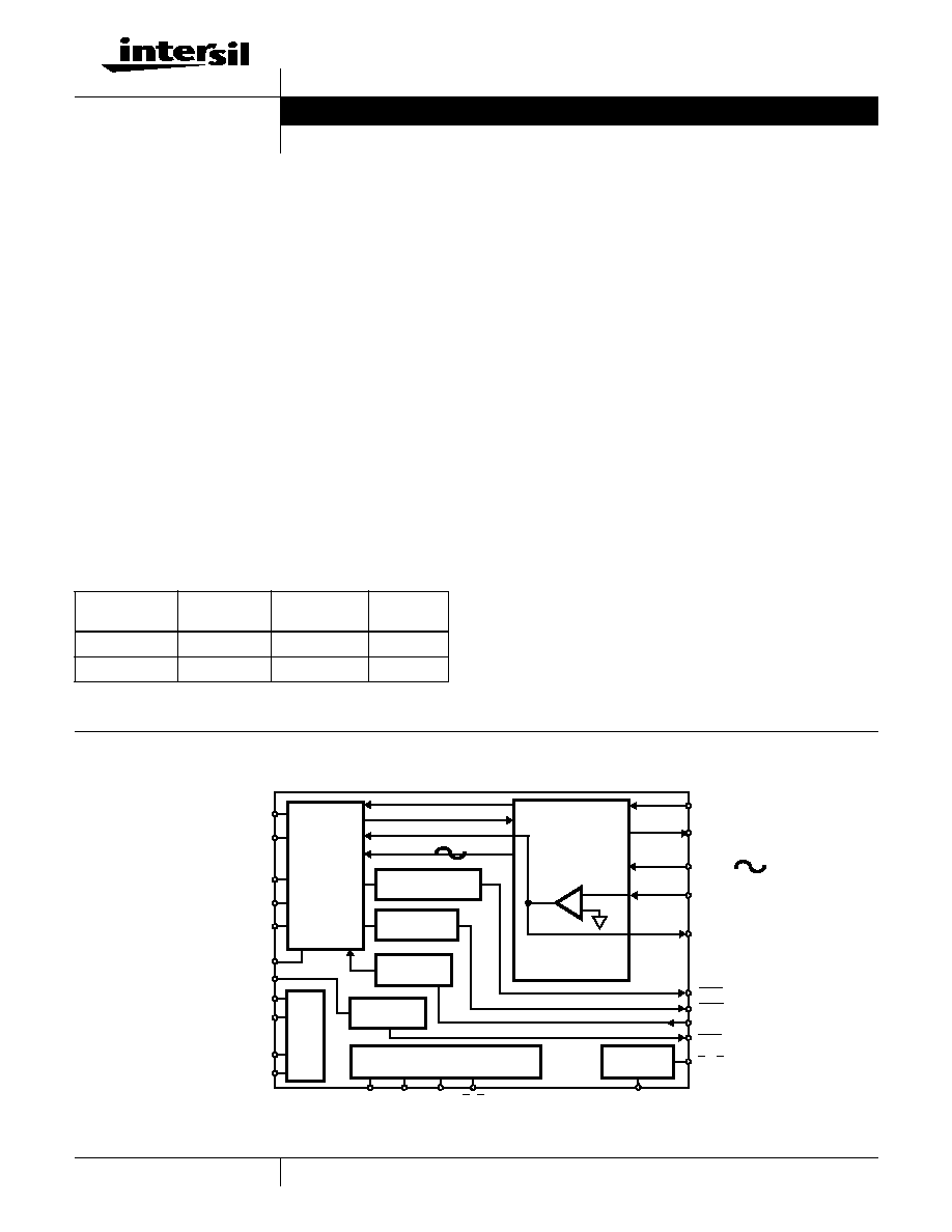
Block Diagram
Ordering Information
PART
NUMBER
TEMP. RANGE
(
o
C)
PACKAGE
PKG. NO.
HC5517BCM
0 to 75
28 Ld PLCC
N28.45
HC5517BCB
0 to 75
28 SOIC
M28.3
TIP FEED
TIP SENSE
RING FEED
RING SENSE 2
V
BAT
V
CC
AGND
BGND
V
RX
V
TX
4-WIRE
INTERFACE
BIAS
- IN 1
OUT 1
V
RING
+
-
LOOP CURRENT
DETECTOR
SHD
RTD
ALM
I
LIMIT
FAULT
DETECTOR
CURRENT
LIMIT
F1
F0
RS
TST
RDI
IIL LOGIC INTERFACE
V
REF
RELAY
DRIVER
RDO
2-WIRE
INTERFACE
RTI
RING TRIP
DETECTOR
RING SENSE 1
Data Sheet
July 1998
File Number
4404.2
62
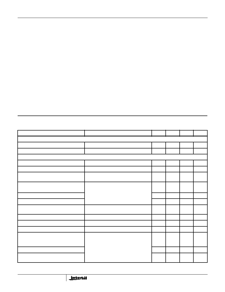
Absolute Maximum Ratings
T
A
= 25
o
C
Thermal Information
Maximum Supply Voltages
(V
CC
) . . . . . . . . . . . . . . . . . . . . . . . . . . . . . . . . . . . . . -0.5V to +7V
(V
CC
)-(V
BAT
) . . . . . . . . . . . . . . . . . . . . . . . . . . . . . . . . . . . . . .90V
Relay Drivers . . . . . . . . . . . . . . . . . . . . . . . . . . . . . . . . -0.5V to +15V
Operating Conditions
Temperature Range
HC5517BCM, HC5517BCB . . . . . . . . . . . . . . . . . . . . 0
o
C to 75
o
C
Relay Drivers . . . . . . . . . . . . . . . . . . . . . . . . . . . . . . . . . +5V to +12V
Positive Power Supply (V
CC
) . . . . . . . . . . . . . . . . . . . . . . . +5V
±
5%
Negative Power Supply (V
BAT
) . . . . . . . . . . . . . . . . . . .-16V to -80V
Thermal Resistance (Typical, Note 1)
JA
(
o
C/W)
PLCC Package . . . . . . . . . . . . . . . . . . . . . . . . . . . . .
55
SOIC Package . . . . . . . . . . . . . . . . . . . . . . . . . . . . .
70
Maximum Junction Temperature, Plastic Packages. . . . . . . . .150
o
C
Maximum Storage Temperature Range . . . . . . . . . . -65
o
C to 150
o
C
Maximum Lead Temperature (Soldering 10s) . . . . . . . . . . . . .300
o
C
(SOIC, PLCC - Lead Tips Only)
Die Characteristics
Transistor Count. . . . . . . . . . . . . . . . . . . . . . . . . . . . . . . . . . . . . . 224
Diode Count. . . . . . . . . . . . . . . . . . . . . . . . . . . . . . . . . . . . . . . . . . 28
Die Dimensions . . . . . . . . . . . . . . . . . . . . . . . . . . . . . . . . . 174 x 120
Substrate Potential. . . . . . . . . . . . . . . . . . . . . . . . . . . . . . . . . . .V
BAT
Process . . . . . . . . . . . . . . . . . . . . . . . . . . . . . . . . . . . . . . . Bipolar-DI
ESD (Human Body Model) . . . . . . . . . . . . . . . . . . . . . . . . . . . .500V
CAUTION: Stresses above those listed in "Absolute Maximum Ratings" may cause permanent damage to the device. This is a stress only rating and operation of the
device at these or any other conditions above those indicated in the operational sections of this specification is not implied
NOTES:
1.
JA
is measured with the component mounted on an evaluation board PC board in free air.
2. All grounds (AGND, BGND) must be applied before V
CC
or V
BAT
. Failure to do so may result in premature failure of the part. If a user wishes
to run separate grounds off a line card, the AGND must be applied first.
Electrical Specifications
Unless Otherwise Specified, Typical Parameters are at T
A
= 25
o
C, Min-Max Parameters are over
Operating Temperature Range, V
BAT
= -24V, V
CC
= +5V, AGND = BGND = 0V. All AC Parameters are specified
at 600
2-Wire Terminating Impedance
PARAMETER
TEST CONDITIONS
MIN
TYP
MAX
UNITS
RINGING TRANSMISSION PARAMETERS
V
RING
Input Impedance
(Note 3)
5.4
k
4-Wire to 2-Wire Gain
V
RING
to Vt-r (Note 3)
40
V/V
AC TRANSMISSION PARAMETERS
RX Input Impedance
300Hz to 3.4kHz (Note 3)
108
k
TX Output Impedance
300Hz to 3.4kHz (Note 3)
20
4-Wire Input Overload Level
300Hz to 3.4kHz R
L
= 1200
, 600
Reference
(Note 3)
+1.0
V
PEAK
2-Wire Return Loss
Matched for 600
(Note 3)
SRL LO
26
35
dB
ERL
30
40
dB
SRL HI
30
40
dB
2-Wire Longitudinal to Metallic Balance
Off Hook
Per ANSI/IEEE STD 455-1976 (Note 3) 300Hz to
3400Hz
40
dB
4-Wire Longitudinal Balance Off Hook
300Hz to 3400Hz (Note 3)
40
dB
Low Frequency Longitudinal Balance
I
LINE
= 40mA T
A
= 25
o
C (Note 3)
10
23
dBrnc
Longitudinal Current Capability
I
LINE
= 40mA T
A
= 25
o
C (Note 3)
40
mA
RMS
Insertion Loss
0dBm at 1kHz, Referenced 600
2-Wire/4-Wire (Includes External Transhybrid
Amplifier with a Gain of 2.4)
±
0.05
±
0.2
dB
4-Wire/2-Wire
±
0.05
±
0.2
dB
4-Wire/4-Wire (Includes External Transhybrid
Amplifier with a Gain of 2.4)
±
0.35
dB
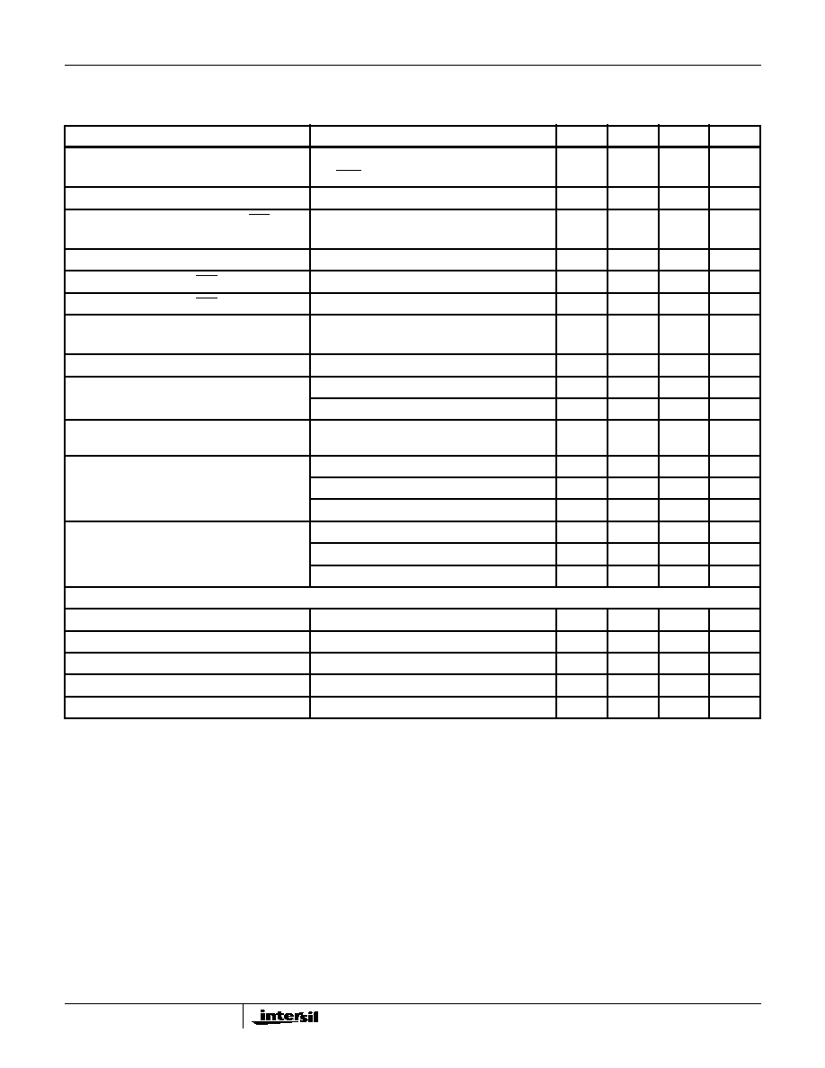
HC5517B

63
Frequency Response
300Hz to 3400Hz (Note 3) Referenced to Absolute
Level at 1kHz, 0dBm Referenced 600
-
±
0.02
±
0.06
dB
Level Linearity
Referenced to -10dBm (Note 3)
2-Wire to 4-Wire and 4-Wire to 2-Wire
+3 to -40dBm
-
-
±
0.08
dB
-40 to -50dBm
-
-
±
0.12
dB
-50 to -55dBm
-
-
±
0.3
dB
Absolute Delay
(Note 3)
2-Wire/4-Wire
300Hz to 3400Hz
-
-
1.0
µ
s
4-Wire/2-Wire
300Hz to 3400Hz
-
-
1.0
µ
s
4-Wire/4-Wire
300Hz to 3400Hz
-
0.95
1.5
µ
s
Transhybrid Loss
V
IN
= 1V
P-P
at 1kHz (Note 3,4)
30
40
-
dB
Total Harmonic Distortion
2-Wire/4-Wire, 4-Wire/2-Wire, 4-Wire/4-Wire
Reference Level 0dBm at 600
300Hz to 3400Hz (Note 3)
-
-
-50
dB
Idle Channel Noise
2-Wire and 4-Wire
(Note 3)
C-Message
-
3
-
dBrnC
Psophometric (Note 3)
-
-87
-
dBmp
Power Supply Rejection Ratio
(Note 3)
30Hz to 200Hz, R
L
= 600
V
CC
to 2-Wire
20
40
-
dB
V
CC
to 4-Wire
20
40
-
dB
V
BAT
to 2-Wire
20
40
-
dB
V
BAT
to 4-Wire
20
50
-
dB
V
CC
to 2-Wire
(Note 3)
200Hz to 16kHz, R
L
= 600
30
40
-
dB
V
CC
to 4-Wire
20
28
-
dB
V
BAT
to 2-Wire
20
50
-
dB
V
BAT
to 4-Wire
20
50
-
dB
DC PARAMETERS
Loop Current Programming
Limit Range
20 (Note
5)
-
60
mA
Accuracy
15
-
-
%
Loop Current During Power Denial
R
L
= 200
-
±
4
±
7
mA
Fault Currents
TIP to Ground (Note 3)
-
30
-
mA
RING to Ground
-
120
-
mA
TIP and RING to Ground (Note 3)
-
150
-
mA
Switch Hook Detection Threshold
-
12
15
mA
Ring Trip Comparator Voltage Threshold
-0.28
-0.24
-0.22
V
Thermal ALARM Output (Note 3)
Safe Operating Die Temperature Exceeded
140
-
160
o
C
Dial Pulse Distortion (Note 3)
-
0.1
0.5
ms
Electrical Specifications
Unless Otherwise Specified, Typical Parameters are at T
A
= 25
o
C, Min-Max Parameters are over
Operating Temperature Range, V
BAT
= -24V, V
CC
= +5V, AGND = BGND = 0V. All AC Parameters are specified
at 600
2-Wire Terminating Impedance (Continued)
PARAMETER
TEST CONDITIONS
MIN
TYP
MAX
UNITS
HC5517B
64
Uncommitted Relay Driver
On Voltage V
OL
I
OL
(RDO) = 30mA
-
0.2
0.5
V
Off Leakage Current
-
±
10
±
100
µ
A
TTL/CMOS Logic Inputs (F0, F1, RS, TST, RDI)
Logic `0' V
IL
0
-
0.8
V
Logic `1' V
IH
2.0
-
5.5
V
Input Current (F0, F1, RS, TST, RDI)
IIH, 0V
V
IN
5V
-
-
-1
µ
A
Input Current (F0, F1, RS, TST, RDI)
IIL, 0V
V
IN
5V
-
-
-100
µ
A
Logic Outputs
Logic `0' V
OL
I
LOAD
= 800
µ
A
-
0.3
0.6
V
Logic `1' V
OH
I
LOAD
= 40
µ
A
2.7
-
-
V
Power Dissipation On Hook
V
CC
= +5V, V
BAT
= -80V, R
LOOP
=
-
300
-
mW
V
CC
= +5V, V
BAT
= -48V, R
LOOP
=
-
150
-
mW
Power Dissipation Off Hook
V
CC
= +5V, V
BAT
= -24V, R
LOOP
= 600
,
I
L
= 25mA
-
280
-
mW
I
CC
V
CC
= +5V, V
BAT
= -80V, R
LOOP
=
-
3
6
mA
V
CC
= +5V, V
BAT
= -48V, R
LOOP
=
-
2
5
mA
V
CC
= +5V, V
BAT
= -24V, R
LOOP
=
-
1.9
4
mA
I
BAT
V
CC
= +5V, V
B
- = -80V, R
LOOP
=
-
3.6
7
mA
V
CC
= +5V, V
B
- = -48V, R
LOOP
=
-
2.6
6
mA
V
CC
= +5V, V
B
- = -24V, R
LOOP
=
-
1.8
4
mA
UNCOMMITTED OP AMP PARAMETERS
Input Offset Voltage
-
±
5
-
mV
Input Offset Current
-
±
10
-
nA
Differential Input Resistance (Note 3)
-
1
-
M
Output Voltage Swing (Note 3)
R
L
= 10k
-
±
3
-
V
P-P
Small Signal GBW (Note 3)
-
1
-
MHz
NOTES:
3. These parameters are controlled by design or process parameters and are not directly tested. These parameters are characterized upon initial
design release, upon design changes which would affect these characteristics, and at intervals to assure product quality and specification com-
pliance.
4. For transhybrid circuit as shown in Figure 3.
5. Application limitation based on maximum switch hook detect limit and metallic currents. Not a part limitation.
Electrical Specifications
Unless Otherwise Specified, Typical Parameters are at T
A
= 25
o
C, Min-Max Parameters are over
Operating Temperature Range, V
BAT
= -24V, V
CC
= +5V, AGND = BGND = 0V. All AC Parameters are specified
at 600
2-Wire Terminating Impedance (Continued)
PARAMETER
TEST CONDITIONS
MIN
TYP
MAX
UNITS
HC5517B
65
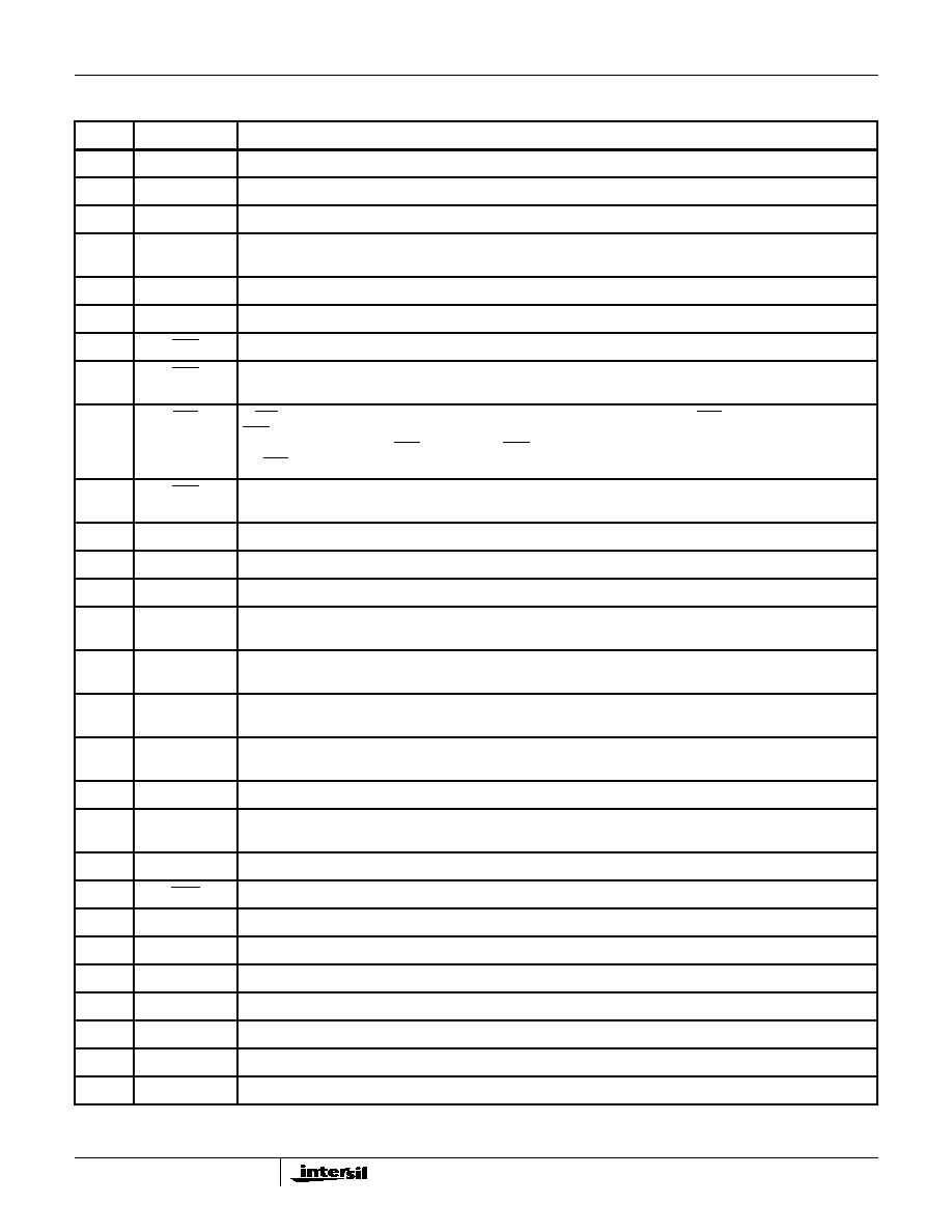
The truth table for the internal logic of the HC5517B is provided
in the above table. This family of ringing SLICs can be config-
ured to support traditional unbalanced ringing and through
SLIC balanced ringing. The device operating states used by
through SLIC ringing applications are loop power denial and
normal feed. During loop power denial, the tip and ring amplifi-
ers are disabled (high impedance) and the DC voltage of each
amplifier approaches ground. The SLIC will not provide current
to the subscriber loop during this mode and will not detect loop
closure. Voice transmission occurs during the normal loop feed
mode. During normal loop feed the SLIC is completely opera-
tional and performs all transmission and supervisory functions.
Power Dissipation
Careful thermal design is required to guarantee that the
maximum junction temperature of 150
o
C of the device is not
exceeded. The junction temperature of the SLIC can be
calculated using:
Where T
A
is maximum ambient temperature and
JA
is
junction to air thermal resistance (and is package depen-
dent). The entire term in parentheses yields the SLIC power
dissipation. The power dissipation of the subscriber loop
does not contribute to device junction temperature and is
subtracted from the power dissipation term. Operating at
85
o
C, the maximum PLCC SLIC power dissipation is 1.18W.
Likewise, the maximum SOIC SLIC power dissipation is
0.92W.
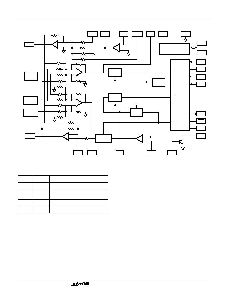
R
R
R
V
RX
OUT 1
R/20
R/2
TIP
TA
R
2R
2R
R
90K
RING
RA
4.5K
25K
25K
100K
100K
4.5K
90K
RF
25
17
12
+2V
TF
14
RF
15
16
26
3
OP AMP
V
RING
V
TX
GM
28
11
RF2
BIAS
NETWORK
AGND
V
CC
IIL LOGIC INTERF
A
C
E
TSD
GK
RFC
SH
F0
F1
RS
ALM
RTD
SHD
TST
V
BAT
-IN 1
13
24
19
2
1
TF
BGND
22
27
4
5
6
9
20
21
7
8
10
R = 108k
R
R
100K
100K
90K
18
SENSE
SENSE 1
RING
SENSE 2
RDO
+
-
+
-
THERM
LTD
SHD
RTD
FAULT
DET
+
-
+
-
+
-
+
-
REF
VB/2
V
REF
NU
I
LIMIT
RDI
RTI
HC5517B DEVICE TRUTH TABLE
F1
F0
STATE
0
0
Loop power Denial Active
0
1
Power Down Latch RESET, Power on
RESET
1
0
RD Active (unbalanced ringing)
1
1
Normal Loop feed
T
J
T
A
JA
I
CC
V
CC
I
BAT
V
BAT
I
LOOP
(
)
2
R
LOOP
∑
(
)
≠
+
(
)
+
=
(EQ. 1)
HC5517B

66
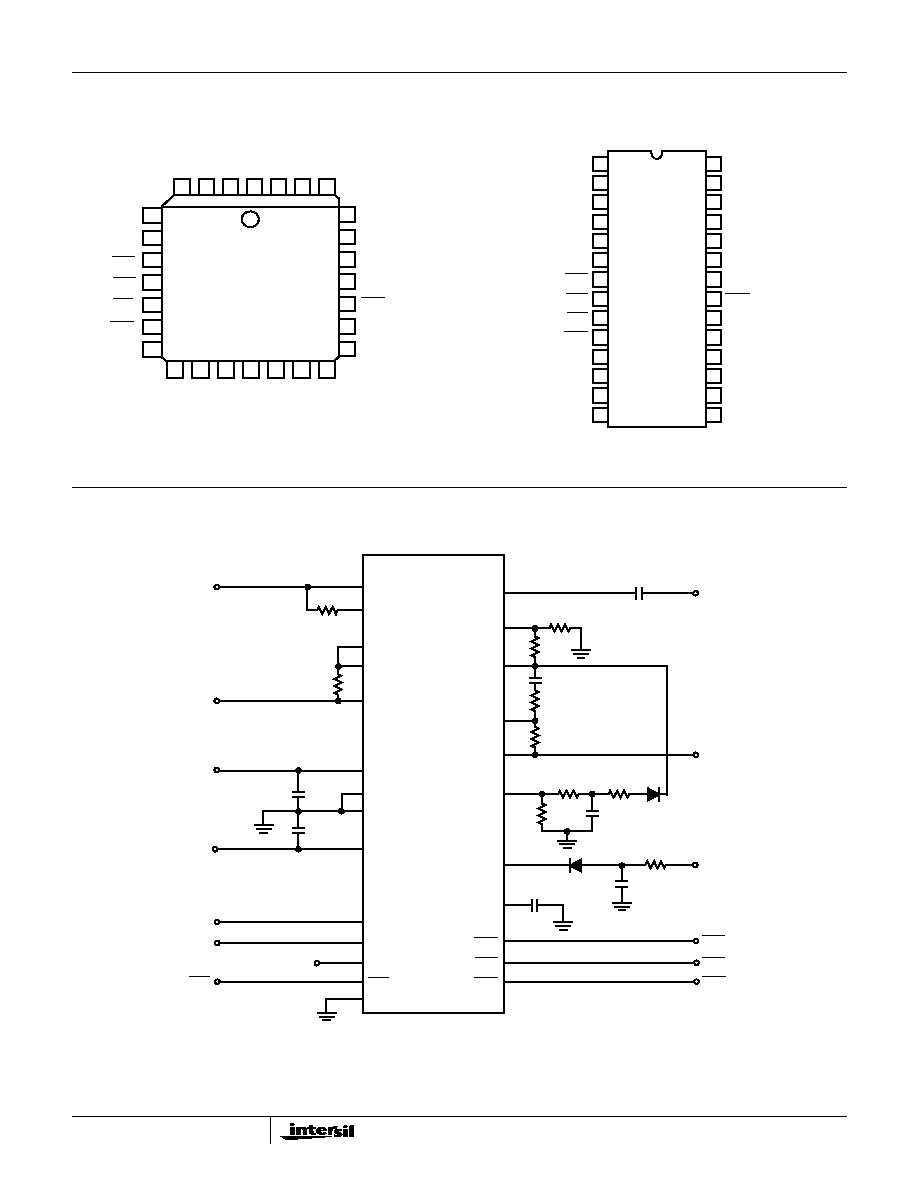
Circuit Operation and Design Information
Through SLIC Ringing
The HC5517B uses linear amplification to produce the ringing
signal. As a result the ringing SLIC can produce sinusoid,
trapezoid or square wave ringing signals. Regardless of the
wave shape, the ringing signal is balanced. The balanced
waveform is another way of saying that the tip and ring DC
potentials are the same during ringing.
Trapezoidal Ringing
The trapezoidal ringing waveform provides a larger RMS
voltage to the handset. Larger RMS voltages to the handset
provide more power for ringing and also increase the loop
length supported by the ringing SLIC.
One set of component values will satisfy the entire ringing
loop range of the SLIC. A single resistor sets the open circuit
RMS ringing voltage, which will set the crest factor of the ring-
ing waveform. The crest factor of the HC5517B ringing wave-
form is independent of the ringing load (REN) and the loop
length. Another robust feature of the HC5517B ringing SLIC is
the ring trip detector circuit. The suggested values for the ring
trip detector circuit cover quite a large range of applications.
The assumptions used to design the trapezoidal ringing
application circuit are listed below:
∑ Loop current limit set to 25mA.
∑ Impedance matching is set to 600
resistive.
∑ 2-wire surge protection is not required.
∑ System able to monitor RTD and SHD.
Logic ringing signal is used to drive RC trapezoid network.
Crest Factor Programming
As previously mentioned, a single resistor is required to set
the crest factor of the trapezoidal waveform. The only design
variable in determining the crest factor is the battery voltage.
The battery voltage limits the peak signal swing and there-
fore directly determines the crest factor.
A set of tables will be provided to allow selection of the crest
factor setting resistor. The tables will include crest factors
below the Bellcore minimum of 1.2 since many ringing SLIC
applications are not constrained by Bellcore requirements.
The RMS voltage listed in the table is the open circuit RMS
voltage generated by the SLIC.
SLIC DESIGN EQUATIONS
FUNCTION
EQUATION
DEFINITION OF TERMS
2-Wire to 4-Wire Gain
V
OUT1
= SLIC 4-wire Output
V
2w
= Voltage across 2-wire load
Z
2W
= 2-Wire Impedance
4-Wire To 2-wire Gain
V
2W
= Voltage Across 2-Wire Load
V
RX
= SLIC 4-Wire Input
Z
2W
= 2-Wire Impedance
Z
SLIC
= SLIC Synthesized Impedance
4-Wire To 4-wire Gain
V
OUT1
= SLIC 4-Wire Output
V
RX
= SLIC 4-Wire Input
Z
2W
= 2-Wire Impedance
Z
SLIC
= SLIC Synthesized Impedance
Loop Current Limit Programming
I
LIMIT
= Programmed Loop Current Limit
R
IL1
= Programming Resistor
R
IL2
= Programming Resistor
Impedance Matching
Z
2W
= 2-Wire Impedance
K = 100
V
OUT1
V
2W
-------------------
200
Z
2w
-----------
≠
R
ZO
R
RF
------------
=
V
2W
V
RX
------------
2
≠
Z
2W
Z
2W
Z
SLIC
+
-----------------------------------
=
V
OUT1
V
RX
-------------------
2
≠
Z
2W
Z
2W
Z
SLIC
+
-----------------------------------
200
Z
2W
------------
R
ZO
R
RF
------------
=
I
LIMIT
0.6
(
)
R
IL1
R
IL2
+
(
)
200xR
IL2
(
)
--------------------------------------------------
=
R
ZO
K
Z
2W
100
≠
(
)
=
R
RF
K 200 2
=
TABLE 1. CREST FACTOR PROGRAMMING RESISTOR FOR
V
BAT
= -80V
RTRAP
CF
RMS
RTRAP
CF
RMS
0
1.10
65.0
825
1.25
57.6
389
1.15
62.6
964
1.30
55.4
640
1.20
60.0
1095
1.35
53.3
TABLE 2. CREST FACTOR PROGRAMMING RESISTOR FOR
V
BAT
= -75V
RTRAP
CF
RMS
RTRAP
CF
RMS
0
1.10
60.9
1010
1.25
53.7
500
1.15
58.3
1190
1.30
51.6
791
1.20
55.9
1334
1.35
49.7
HC5517B
67
The voltages listed in the tables are driven from a logic
source that will not drive the ringing input negative. If the
ringing input is driven negative by 200mV, the peak-to-peak
ringing amplitudes can be increased.
Ringing Voltage Limiting Factors
As the load impedance decreases (increasing REN), the
source impedance of the SLIC during ringing slightly
attenuates the ringing signal.
If additional surge protection resistance must be used with
the trapezoidal circuit, the loop length performance of the
circuit will decrease proportionally to the added resistance
in the Tip and Ring leads. For example if 30
protection
resistors is used in each of the Tip and Ring leads, the ring-
ing loop length will decrease by a total of 60
.
Low Level Ringing Interface
The trapezoidal application circuit only requires a cadenced
logic signal applied to the wave shaping RC network to
achieve ringing. When not ringing, the logic signal should be
held low. When the logic signal is low, Tip will be near
ground and Ring will be near battery. When the logic signal
is high, Tip will be near battery and Ring will be near ground.
Loop Detector Interface
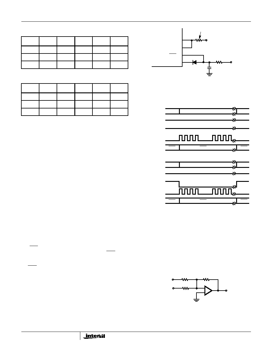
The RTD output should be monitored for off hook detection
during the ringing period. At all other times, the SHD should
be monitored for off hook detection. The application circuit
can be modified to redirect the ring trip information through
the SHD interface. The change can be made by rewiring the
application circuit, adding a pullup resistor to pin 23 and set-
ting F0 low for the entire duration of the ringing period. The
modifications to the application circuit for the single detector
interface are shown in Figure 1.
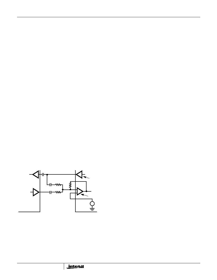
SLIC Operating State During Ringing
The SLIC control pin F1 should always be a logic high during
ringing. The control pin F0 will either be a constant logic high
(two detector interface) or a logic low (single detector
interface). Figure 2 shows the control interface for the dual
detector interface and the single detector interface.
Additional Application Information
Transhybrid Balance
Since the receive signal and its echo are 180 degrees out of
phase, the summing node of an operational amplifier can be
used to cancel the echo. Nearly all CODECs have an inter-
nal amplifier for echo cancellation. The circuit in Figure 3
shows the cancellation amplifier circuit.
TABLE 3. CREST FACTOR PROGRAMMING RESISTOR FOR
V
BAT
= -65V
RTRAP
CF
RMS
RTRAP
CF
RMS
0
1.10
52.5
1330
1.25
45.9
660
1.15
49.8
1600
1.30
44.1
1040
1.20
47.8
1800
1.35
42.5
TABLE 4. CREST FACTOR PROGRAMMING RESISTOR FOR
V
BAT
= -60V
RTRAP
CF
RMS
RTRAP
CF
RMS
0
1.10
48.2
1460
1.25
42.0
740
1.15
45.6
1760
1.30
40.4
1129
1.20
43.7
2030
1.35
38.8
HC5517B
V
RING
24
C
TRAP
V
RING
R
TRAP
D
TRAP
RDO 21
RDI 20
NU 23
ADDITIONAL PULL UP RESISTOR
V
CC
FIGURE 1. APPLICATION CIRCUIT WIRING FOR SINGLE
LOOP DETECTOR INTERFACE
FIGURE 2. DETECTOR LOGIC INTERFACES
F1
RINGING
ACTIVE
ACTIVE
F0
V
RING
MODE
(LOGIC HI)
(LOGIC HI)
RTD
SHD
SHD
VALID DET
F1
RINGING
ACTIVE
ACTIVE
F0
V
RING
MODE
(LOGIC HI)
(LOGIC HI)
SHD
SHD
SHD
VALID DET
(SINGLE DETECTOR INTERFACE)
(DUAL DETECTOR INTERFACE)
FIGURE 3. TRANSHYBRID AMPLIFIER CIRCUIT
+
-
R
F
R
B
R
A
V
RX
V
OUT1
VO
HC5517B
68
When the SLIC is matched to a 600
load and only the sense
resistors are used, the 4-wire to 4-wire gain is equal to 5/12 as
predicted by the design equations. Therefore, by configuring
the transhybrid amplifier with a gain of 2.4 in the echo path,
cancellation can be achieved. The following equations:
Substituting the fact that V
OUT1
is -5/12 of V
RX
Since cancellation implies that under these conditions, the
output V
O
should be zero, set Equation 2 equal to zero and
solve for R
B
.
Another outcome of the transhybrid gain selection is the
2-wire to 4-wire gain of the SLIC as seen by the CODEC.
The 5/12 voltage gain in the transmit path is relevant to the
receive input as well as any signals from the 2-wire side.
Therefore by setting the V
OUT1
gain to 2.4 in the previous
analysis, the 2-wire to 4-wire gain was set to unity.
Single Supply CODEC Interface
The majority of CODECs that interface to the ringing SLIC
operate from a single +5V supply and ground. Figure 4
shows the circuitry required to properly interface the ringing
SLIC to the single supply CODEC.
The CODEC signal names may vary from different manufac-
turers, but the function provided will be the same. The DC
reference from the CODEC is used to bias the analog sig-
nals between +5V and ground. The capacitors are required
so that the DC gain is unity for proper biasing from the
CODEC reference. Also, the capacitors block DC signals
that may interfere with SLIC or CODEC operation.
Layout Guidelines and Considerations
The printed circuit board trace length to all high impedance
nodes should be kept as short as possible. Minimizing length
will reduce the risk of noise or other unwanted signal pickup.
The short lead length also applies to all high gain inputs. The
set of circuit nodes that can be categorized as such are:
∑ V
RX
pin 27, the 4-wire voice input (low gain input).
∑ -IN1 pin 13, the inverting input of the internal amplifier.
∑ V
REF
pin 3, the noninverting input to ring feed amplifier.
∑ V
RING
pin 24, the 20V/V input for the ringing signal.
For multi layer boards, the traces connected to tip should not
cross the traces connected to ring. Since they will be carry-
ing high voltages, and could be subject to lightning or surge
depending on the application, using a larger than minimum
trace width is advised.
The 4-wire transmit and receive signal paths should not
cross. The receive path is any trace associated with the V
RX
input and the transmit path is any trace associated with V
TX
output. The physical distance between the two signal paths
should be maximized to reduce crosstalk, or separated by a
ground trace.
The operating mode control signals and detector outputs
should be routed away from the analog circuitry. Though
the digital signals are nearly static, care should be taken to
minimize coupling of the sharp digital edges to the analog
signals.
The part has two ground pins, one is labeled AGND and the
other BGND. Both pins should be connected together as
close as possible to the SLIC. If a ground plane is available,
then both AGND and BGND should be connected directly to
the ground plane.
A ground plane that provides a low impedance return path
for the supply currents should be used. A ground plane
provides isolation between analog and digital signals. If the
layout density does not accommodate a ground plane, a
single point grounding scheme should be used.
V
O
V
RX
R
F
R
A
--------
V
OUT1
R
F
R
B
--------
+
≠
=
(EQ. 2)
V
O
V
RX
R
F
R
A
--------
V
RX
5
12
------
≠
R
F
R
B
--------
≠
≠
=
(EQ. 3)
R
B
R
A
2.4
--------
=
(EQ. 4)
FIGURE 4. SINGLE SUPPLY CODEC INTERFACE
+
-
+
-
R
F
R
B
R
A
HC5517B
CODEC
+2.5V
V
RX
V
OUT1
RX OUT
TX IN
HC5517B
69
Pin Descriptions
PLCC
SYMBOL
DESCRIPTION
1
AGND
Analog Ground - Serves as a reference for the transmit output and receive input terminals.
2
V
CC
Positive Voltage Source - normally +5V DC.
3
V
REF
An external voltage connected to this pin will override the internal V
BAT
/2 reference.
4
F1
Power Denial - An active low TTL compatible logic control input. When enabled, the output of the ring amplifier will
ramp close to the output voltage of the tip amplifier.
5
F0
TTL compatible logic control input that controls multiplexing of the detector outputs.
6
RS
TTL compatible logic control input that must be tied high for proper SLIC operation.
7
SHD
Switch Hook Detection - An active low TTL compatible logic output. Indicates an off-hook condition.
8
RTD
Ring Trip Detection - An active low TTL compatible logic output. Indicates an off-hook condition when the phone is
ringing. May be used to indicate ring trip or ground key detection.
9
TST
A TTL logic input. A low on this pin will keep the SLIC in a power down mode. The TST pin, in conjunction with the
ALM pin, can provide thermal shutdown protection for the SLIC. Thermal shutdown is implemented by a system
controller that monitors the ALM pin. When the ALM pin is active (low), the system controller issues a command to
the TST pin (low) to power down the SLIC. The timing of the thermal recovery is controlled by the system controller.
10
ALM
A TTL compatible active low output which responds to the thermal detector circuit when a safe operating die
temperature has been exceeded.
11
I
LIMIT
Loop Current Limit - used with V
TX
to set the short loop current limiting conditions.
12
OUT1
The 4-wire output of the SLIC.
13
-IN1
The inverting input of the impedance matching amplifier. The non-inverting input is internally connected to AGND.
14
TIP SENSE
An analog input connected to the TIP (more positive) side of the subscriber loop through a feed resistor. Functions
with the RING terminal to receive voice signals and for loop monitoring purpose.
15
RING SENSE 1
An analog input connected to the RING (more negative) side of the subscriber loop through a feed resistor. Functions
with the TIP terminal to receive voice signals and for loop monitoring purposes.
16
RING SENSE 2
This is an internal sense mode that must be tied to RING SENSE 1 for proper SLIC operation. Also used during
unbalanced ringing.
17
V
RX
Receive Input, 4-Wire Side - A high impedance analog input. AC signals appearing at this input drive the Tip Feed
and Ring Feed amplifiers differentially.
18
NU
Not used in this application. This pin should be left floating.
19
V
TX
A low impedance analog voltage output which is proportional to the subscriber loop current. Since the DC level of
this output varies with loop current, capacitive coupling to IN1- is necessary.
20
RDI
TTL compatible input to drive the ring relay driver during unbalanced ringing.
21
RDO
Open collector relay driver used during unbalanced ringing.
22
BGND
Battery Ground - All loop current and some quiescent current flows from this terminal.
23
NU
Not used in this application. This pin should be either grounded or left floating.
24
V
RING
Low level ringing signal input.
25
TF
Output of the tip line feed amplifier.
26
RF
Output of the ring line feed amplifier.
27
V
BAT
The negative battery source, all loop current flows into this terminal.
28
RTI
Ring Trip Input - This pin is connected to the external negative peak detector output for ring trip detection.
HC5517B
70
Trapezoidal Ringing Application Circuit
Pinouts
HC5517B (PLCC)
TOP VIEW
HC5517B (SOIC)
TOP VIEW
RT
I
RF
TF
V
RING
V
TX
NU
V
RX
RING SENSE 2
RING SENSE 1
V
BA
T
BGND
RDO
NU
RDI
V
CC
A
GND
RS
I
LIMIT
OUT 1
-IN 1
TIP SENSE
F0
V
REF
F1
SHD
RTD
TST
ALM
5
6
7
8
9
10
11
12
13
14
15
16
17
18
1
2
3
4
19
20
21
22
23
24
25
26
27
28
AGND
V
CC
V
REF
F1
F0
RS
SHD
RTD
TST
ALM
I
LIMIT
OUT 1
-IN 1
TIP SENSE
RTI
RF
TF
V
RING
NU
RDO
V
TX
NU
V
RX
RING SENSE 2
RING SENSE 1
V
BAT
BGND
RDI
28
27
26
25
24
23
22
21
20
19
18
17
16
15
1
2
3
4
5
6
7
8
9
10
11
12
13
14
28
27
26
25
24
23
22
21
20
19
18
17
16
15
1
2
3
4
5
6
7
8
9
10
11
12
13
14
TIP
V
RX
I
LIMIT
V
TX
RF
TF
TIP SENSE
R
S1
R
IL1
C
AC
R
RF
HC5517B
V
REF
V
CC
RING
SHD
RTD
ALM
TST
RS
R
RT3
R
RT2
-IN1
OUT1
V
RING
RTI
V
BAT
BGND
AGND
V
CC
RING SENSE 1
RING SENSE 2
R
S2
C
PS1
C
PS2
R
ZO
C
TRAP
C
IL
C
RT
C
RX
R
IL2
V-REC
FIGURE 5. TRAPEZOIDAL RINGING APPLICATION CIRCUIT
R
RT1
V-XMIT
V
RING
V
BAT
F0
F1
SHD
RTD
ALM
F1
F0
V
CC
TST
RDI
R
TRAP
D
RT
D
TRAP
U1
24
3
28
12
7
8
10
13
19
11
17
14
25
26
16
15
2
15
22
27
4
5
6
9
20
HC5517B
71
All Intersil semiconductor products are manufactured, assembled and tested under ISO9000 quality systems certification.
Intersil semiconductor products are sold by description only. Intersil Corporation reserves the right to make changes in circuit design and/or specifications at any time with-
out notice. Accordingly, the reader is cautioned to verify that data sheets are current before placing orders. Information furnished by Intersil is believed to be accurate and
reliable. However, no responsibility is assumed by Intersil or its subsidiaries for its use; nor for any infringements of patents or other rights of third parties which may result
from its use. No license is granted by implication or otherwise under any patent or patent rights of Intersil or its subsidiaries.
For information regarding Intersil Corporation and its products, see web site http://www.intersil.com
Sales Office Headquarters
NORTH AMERICA
Intersil Corporation
P. O. Box 883, Mail Stop 53-204
Melbourne, FL 32902
TEL: (407) 724-7000
FAX: (407) 724-7240
EUROPE
Intersil SA
Mercure Center
100, Rue de la Fusee
1130 Brussels, Belgium
TEL: (32) 2.724.2111
FAX: (32) 2.724.22.05
ASIA
Intersil (Taiwan) Ltd.
7F-6, No. 101 Fu Hsing North Road
Taipei, Taiwan
Republic of China
TEL: (886) 2 2716 9310
FAX: (886) 2 2715 3029
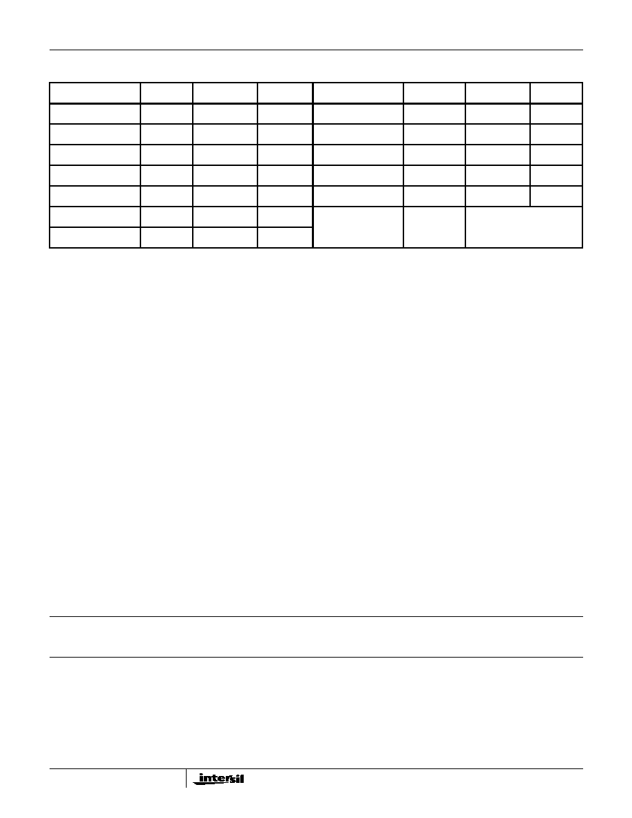
HC5517B Trapezoidal Ringing Application Circuit Parts List
COMPONENT
VALUE
TOLERANCE
RATING
COMPONENT
VALUE
TOLERANCE
RATING
U1 - Ringing SLIC
HC5517B
N/A
N/A
R
IL2
7.68k
1%
1
/
8
W
R
S1
, R
S2
49.9
1%
1
/
2
W
R
TRAP
User-Defined
1%
1
/
8
W
R
ZO
, R
IL1
56.2k
1%
1
/
8
W
C
PS1
, C
PS2
0.1
µ
F
10%
100V
R
RT1
49.9k
1%
1
/
8
W
C
IL
, C
RT
, C
AC
, C
RX
0.47
µ
F
10%
50V
R
RT2
1.5M
1%
1
/
8
W
C
TRAP
4.7
µ
F
10%
10V
R
RT3
51.1k
1%
1
/
8
W
D
RT
, D
TRAP
1N914
Generic Rectifier Diode
R
RF
45.3k
1%
1
/
8
W
HC5517B