TM
4-1
File Number
4519.5
HC55180, HC55181, HC55182, HC55183, HC55184
Extended Reach Ringing SLIC Family
The RSLIC18 family of
ringing subscriber line
interface circuits (RSLIC)
supports analog Plain Old
Telephone Service (POTS) in
short and medium loop length, wireless and wireline
applications. Ideally suited for remote subscriber units, this
family of products offers flexibility to designers with high
ringing voltage and low power consumption system
requirements.
The RSLIC18 family operates to 100V which translates
directly to the amount of ringing voltage supplied to the end
subscriber. With the high operating voltage, subscriber loop
lengths can be extended to 500
(i.e., 5,000 feet) and
beyond.
Other key features across the product family include: low
power consumption, ringing using sinusoidal or trapezoidal
waveforms, robust auto-detection mechanisms for when
subscribers go on or off hook, and minimal external discrete
application components. Integrated test access features are
also offered on selected products to support loopback
testing as well as line measurement tests.
There are five product offerings in the RSLIC18 family:
HC55180, HC55181, HC55182, HC55183 and HC55184.
The architecture for this family is based on a voltage feed
amplifier design using low fixed loop gains to achieve high
analog performance with low susceptibility to system
induced noise.
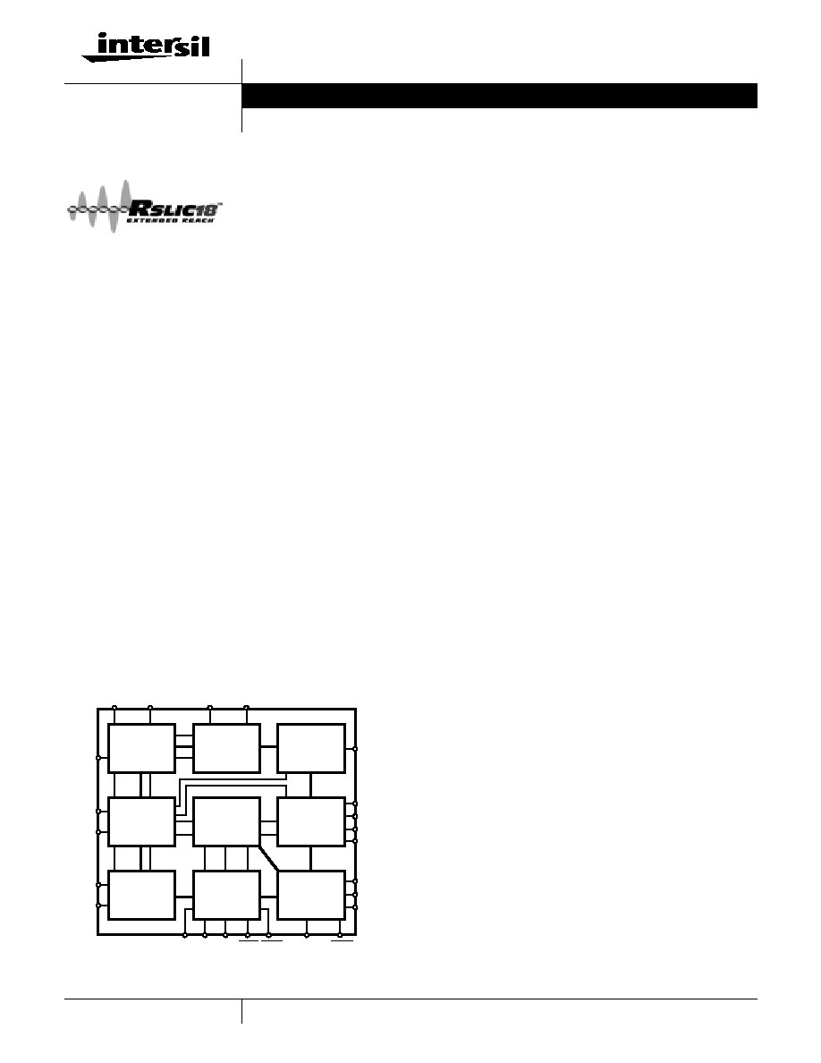
Block Diagram
Features
� Battery Operation to 100V
� Low Standby Power Consumption of 50mW
� Peak Ringing Amplitude 95V, 5 REN
� Sinusoidal or Trapezoidal Ringing Capability
� Integrated CODEC Ringing Interface
� Integrated MTU DC Characteristics
� Low External Component Count
� Pulse Metering and On Hook Transmission
� Tip Open Ground Start Operation
� Thermal Shutdown with Alarm Indicator
� 28 Lead Surface Mount Packaging
� Dielectric Isolated (DI) High Voltage Design
� HC55180
- Silent Polarity Reversal
- 53dB Longitudinal Balance
- Loopback Test Capability
� HC55181
- Integrated Battery Switch
- Silent Polarity Reversal
- 53dB Longitudinal Balance
- Loopback and Test Access Capability
� HC55182
- Integrated Battery Switch
- 53dB Longitudinal Balance
- Loopback and Test Access Capability
� HC55183
- Integrated Battery Switch
- 45dB Longitudinal Balance
� HC55184
- Integrated Battery Switch
- Silent Polarity Reversal
- 45dB Longitudinal Balance
Applications
� Wireless Local Loop (WLL)
� Digital Added Main Line (DAML)/Pairgain
� Integrated Services Digital Network (ISDN)
� Small Office Home Office (SOHO) PBX
� Cable/Computer Telephony
Related Literature
� AN9814, User's Guide for Development Board
� AN9824, Modeling of the AC Loop
� AN TBD, Interfacing to DSP CODECs
VRS
VRX
VTX
-IN
VFB
F2
F1
F0
ILIM
TIP
RING
SW+
SW-
RTD RD
DET ALM
RINGING
PORT
4-WIRE
PORT
CONTROL
LOGIC
BATTERY
SWITCH
TRANSMIT
SENSING
DETECTOR
LOGIC
DC
CONTROL
2-WIRE
PORT
TEST
ACCESS
E0
POL
CDC
VBH
VBL
BSEL
SWC
Data Sheet
September 2000
CAUTION: These devices are sensitive to electrostatic discharge; follow proper IC Handling Procedures.
1-888-INTERSIL or 321-724-7143
|
Intersil and Design is a trademark of Intersil Corporation.
|
Copyright
�
Intersil Corporation 2000
RSLIC18TM is a trademark of Intersil Corporation.

4-2
Ordering Information (PLCC Package Only)
PART NUMBER
100V
85V
BAT
SW
POL
REV
FULL
TEST
LOOP
BACK
ONLY
LB = 53dB
LB = 58dB
TEMP.
RANGE (
o
C)
PACKAGE
PACKAGE
NO.
HC55180CIM
�
�
�
�
-40 to 85
28 Ld PLCC
N28.45
HC55180DIM
�
�
�
�
-40 to 85
28 Ld PLCC
N28.45
HC55181CIM
�
�
�
�
�
-40 to 85
28 Ld PLCC
N28.45
HC55181DIM
�
�
�
�
�
-40 to 85
28 Ld PLCC
N28.45
HC55182CIM
�
�
�
�
-40 to 85
28 Ld PLCC
N28.45
HC55182DIM
�
�
�
�
-40 to 85
28 Ld PLCC
N28.45
HC55183ECM
75V
�
45dB
0 to 70
28 Ld PLCC
N28.45
HC55184ECM
75V
�
�
45dB
0 to 70
28 Ld PLCC
N28.45
HC5518XEVAL1
Evaluation board platform, including CODEC.
Device Operating Modes
OPERATING
MODE
F2
F1
F0
E0 = 1 E0 = 0
DESCRIPTION
HC55180
HC55181
HC55182
HC55183
HC55184
Low Power
Standby
0
0
0
SHD
GKD
MTU compliant standby
mode with active loop
detector.
�
�
�
�
�
Forward Active
0
0
1
SHD
GKD
Forward battery loop feed.
�
�
�
�
�
Unused
0
1
0
n/a
n/a
This is a reserved internal
test mode.
Reverse Active
0
1
1
SHD
GKD
Reverse battery loop feed.
�
�
�
Ringing
1
0
0
RTD
RTD
Balanced ringing mode
supporting both sinusoidal,
trapezoidal and ringing
waveforms with DC offset.
�
�
�
�
�
Forward Loop
Back
1
0
1
SHD
GKD
Internal device test mode.
�
�
�
Tip Open
1
1
0
SHD
GKD
Tip amplifier disabled and
ring amplifier enabled.
Intended for PBX type
applications.
�
�
�
Power Denial
1
1
1
n/a
n/a
Device shutdown.
�
�
�
�
�
HC55180, HC55181, HC55182, HC55183, HC55184
4-3
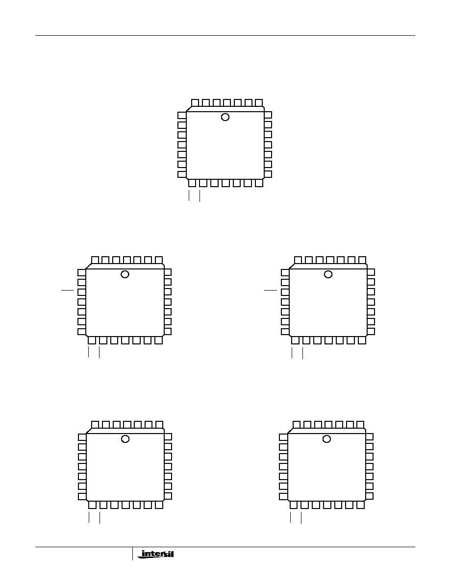
Pinouts
HC55180
(PLCC)
TOP VIEW
HC55181
(PLCC)
TOP VIEW
HC55182
(PLCC)
TOP VIEW
HC55183
(PLCC)
TOP VIEW
HC55184
(PLCC)
TOP VIEW
RING
ILIM
RTD
CDC
VRX
VRS
POL
NC
NC
RD
-IN
VFB
VCC
VTX
BGND
TIP
NC
E0
DET
ALM
A
GND
NC
VBL
VBH
NC
F2
F1
F0
5
6
7
8
9
10
11
12
13
14
15
16
17
18
1
2
3
4
19
20
21
22
23
24
25
26
27
28
RING
ILIM
RTD
CDC
VRX
VRS
POL
NC
BSEL
RD
-IN
VFB
VCC
VTX
BGND
TIP
SW-
E0
DET
ALM
A
GND
SW+
VBL
VBH
SWC
F2
F1
F0
5
6
7
8
9
10
11
12
13
14
15
16
17
18
1
2
3
4
19
20
21
22
23
24
25
26
27
28
RING
ILIM
RTD
CDC
VRX
VRS
NC
NC
BSEL
RD
-IN
VFB
VCC
VTX
BGND
TIP
SW-
E0
DET
ALM
A
GND
SW+
VBL
VBH
SWC
F2
F1
F0
5
6
7
8
9
10
11
12
13
14
15
16
17
18
1
2
3
4
19
20
21
22
23
24
25
26
27
28
RING
ILIM
RTD
CDC
VRX
VRS
NC
NC
BSEL
RD
-IN
VFB
VCC
VTX
BGND
TIP
NC
E0
DET
ALM
A
GND
NC
VBL
VBH
NC
F2
F1
F0
5
6
7
8
9
10
11
12
13
14
15
16
17
18
1
2
3
4
19
20
21
22
23
24
25
26
27
28
RING
ILIM
RTD
CDC
VRX
VRS
POL
NC
BSEL
RD
-IN
VFB
VCC
VTX
BGND
TIP
NC
E0
DET
ALM
A
GND
NC
VBL
VBH
NC
F2
F1
F0
5
6
7
8
9
10
11
12
13
14
15
16
17
18
1
2
3
4
19
20
21
22
23
24
25
26
27
28
HC55180, HC55181, HC55182, HC55183, HC55184

4-4
Absolute Maximum Ratings
T
A
= 25
o
C
Thermal Information
Maximum Supply Voltages
V
CC
. . . . . . . . . . . . . . . . . . . . . . . . . . . . . . . . . . . . . -0.5V to +7V
V
CC
- V
BAT
(180, 181, 182) . . . . . . . . . . . . . . . . . . . . . . . . . 110V
V
CC
- V
BAT
(183, 184) . . . . . . . . . . . . . . . . . . . . . . . . . . . . . . 85V
Uncommitted Switch Voltage . . . . . . . . . . . . . . . . . . . . . . . -110V
Maximum Tip/Ring Negative Voltage Pulse (Note 18) . . . . . . . -115V
Maximum Tip/Ring Positive Voltage Pulse (Note 18). . . . . . . . . . .8V
ESD (Human Body Model). . . . . . . . . . . . . . . . . . . . . . . . . . . . 500V
Operating Conditions
Temperature Range
Industrial (I Suffix) . . . . . . . . . . . . . . . . . . . . . . . . . -40
o
C to 85
o
C
Commercial (C Suffix) . . . . . . . . . . . . . . . . . . . . . . . . 0
o
C to 75
o
C
Positive Power Supply (V
CC
) . . . . . . . . . . . . . . . . . . . . . . . +5V
�
5%
Negative Power Supply (V
BH
, V
BL
) (180, 181, 182) . -16V to -100V
Negative Power Supply (V
BH
, V
BL
) (183, 184) . . . . . . -24V to -75V
Uncommitted Switch (loop back or relay driver). . . . . . +5V to -100V
Thermal Resistance (Typical, Note 1)
JA
(
o
C/W)
PLCC Package . . . . . . . . . . . . . . . . . . . . . . . . . . . . .
53
Maximum Junction Temperature Plastic . . . . . . . . . . . . . . . . 150
o
C
Maximum Storage Temperature Range . . . . . . . . . . -65
o
C to 150
o
C
Maximum Lead Temperature (Soldering 10s) . . . . . . . . . . . . 300
o
C
(PLCC - Lead Tips Only)
Die Characteristics
Substrate Potential. . . . . . . . . . . . . . . . . . . . . . . . . . . . . . . . . . V
BAT
Process . . . . . . . . . . . . . . . . . . . . . . . . . . . . . . . . . . . . . . Bipolar-DI
CAUTION: Stresses above those listed in "Absolute Maximum Ratings" may cause permanent damage to the device. This is a stress only rating and operation of the
device at these or any other conditions above those indicated in the operational sections of this specification is not implied.
NOTE:
1.
JA
is measured with the component mounted on an evaluation PC board in free air.
Electrical Specifications
Unless Otherwise Specified, T
A
= 0
o
C to 70
o
C for the HC55183, 184 only, all others -40
o
C to 85
o
C, V
BL
= -24V,
V
BH
= -100V, -85V or -75V, V
CC
= +5V, AGND = BGND = 0V, loop current limit = 25mA. All AC Parameters are
specified at 600
2-wire terminating impedance over the frequency band of 300Hz to 3.4kHz. Protection
resistors = 0
. These parameters apply generically to each product offering.
PARAMETER
TEST CONDITIONS
MIN
TYP
MAX
UNITS
RINGING PARAMETERS (Note 2)
VRS Input Impedance (Note 3)
480
-
-
k
Differential Ringing Gain
VRS to 2-Wire, R
LOAD
=
(Note 4)
78
80
82
V/V
4-Wire to 2-Wire Ringing Off Isolation
Active mode, referenced to VRS input.
-
60
-
dB
2-Wire to 4-Wire Transmit Isolation
Ringing mode referenced to the differential ringing
amplitude.
-
60
-
dB
AC TRANSMISSION PARAMETERS (Notes 5, 6)
Receive Input Impedance (Note 3)
160
-
-
k
Transmit Output Impedance (Note 3)
-
-
1
4-Wire Port Overload Level
THD = 1%
3.1
3.5
-
V
PK
2-Wire Port Overload Level
THD = 1%
3.1
3.5
-
V
PK
2-Wire Return Loss
f = 300Hz
-
26
-
dB
f = 1kHz
-
32
-
dB
f = 2.3kHz
-
21
-
dB
f = 3.4kHz
-
17
-
dB
Longitudinal Current Capability (Per Wire) (Note 3)
Test for False Detect
20
-
-
mA
RMS
Test for False Detect, Low Power Standby
10
-
-
mA
RMS
4-Wire to 2-Wire Insertion Loss
-0.20
0.0
+0.30
dB
2-Wire to 4-Wire Insertion Loss
-6.22
-6.02
-5.82
dB
4-Wire to 4-Wire Insertion Loss
-6.32
-6.02
-5.82
dB
Idle Channel Noise 2-Wire
C-Message
-
16
19
dBrnC
Psophometric
-
-73.5
-71
dBmp
Idle Channel Noise 4-Wire
C-Message
-
10
13
dBrnC
Psophometric
-
-79.5
-77
dBmp
HC55180, HC55181, HC55182, HC55183, HC55184

4-5
DC PARAMETERS (Note 6)
Loop Current Limit Programming Range (Note 5)
Max Low Battery = -52V
15
-
45
mA
Loop Current During Low Power Standby
Forward polarity only.
18
-
26
mA
LOOP DETECTORS AND SUPERVISORY FUNCTIONS
Switch Hook Programming Range
5
-
15
mA
Switch Hook Programming Accuracy
Assumes 1% external programming resistor
-
2
10
%
Dial Pulse Distortion
-
1.0
-
%
Ring Trip Comparator Threshold
2.4
2.7
3.0
V
Ring Trip Programming Current Accuracy
-
-
10
%
Ground Key Threshold
-
12
-
mA
Thermal Alarm Output
IC junction temperature
-
175
-
o
C
LOGIC INPUTS (F0, F1, F2, E0, SWC, BSEL)
Input Low Voltage
-
-
0.8
V
Input High Voltage
2.0
-
-
V
Input Low Current
V
IL
= 0.4V
-20
-
-
�
A
Input High Current
V
IH
= 2.4V
-
-
5
�
A
LOGIC OUTPUTS (DET, ALM)
Output Low Voltage
I
OL
= 5mA
-
-
0.4
V
Output High Voltage
I
OH
= 100
�
A
2.4
-
-
V
POWER SUPPLY REJECTION RATIO
V
CC
to 2-Wire
f = 300Hz
-
40
-
dB
f = 1kHz
-
35
-
dB
f = 3.4kHz
-
28
-
dB
V
CC
to 4-Wire
f = 300Hz
-
45
-
dB
f = 1kHz
-
43
-
dB
f = 3.4kHz
-
33
-
dB
V
BL
to 2-Wire
300Hz
f
3.4kHz
-
30
-
dB
V
BL
to 4-Wire
300Hz
f
3.4kHz
-
35
-
dB
V
BH
to 2-Wire
300Hz
f
3.4kHz
-
33
-
dB
V
BH
to 4-Wire
300Hz
f
1kHz
-
40
-
dB
1kHz
<
f
3.4kHz
-
45
-
dB
NOTES:
2. These parameters are specified at high battery operation. For the HC55180 the external supply is set to high battery voltage, for the HC55181,
HC55182, HC55183 and HC55184, BSEL = 1.
3. These parameters are controlled via design or process parameters and are not directly tested. These parameters are characterized upon initial
design release and upon design changes which would affect these characteristics.
4. Differential Ringing Gain is measured with VRS = 0.795 V
RMS
for -100V devices, VRS = 0.663 V
RMS
for -85V devices and VRS = 0.575 V
RMS
for -75V devices.
5. These parameters are specified at low battery operation. For the HC55180, the external supply is set to low battery voltage, for the HC55181,
HC55182, HC55183 and HC55184, BSEL = 0.
6. Forward Active and Reverse Active performance is guaranteed for the HC55180, HC55181 and HC55184 devices only. The HC55182 and
HC55183 are specified for Forward Active operation only.
Electrical Specifications
Unless Otherwise Specified, T
A
= 0
o
C to 70
o
C for the HC55183, 184 only, all others -40
o
C to 85
o
C, V
BL
= -24V,
V
BH
= -100V, -85V or -75V, V
CC
= +5V, AGND = BGND = 0V, loop current limit = 25mA. All AC Parameters are
specified at 600
2-wire terminating impedance over the frequency band of 300Hz to 3.4kHz. Protection
resistors = 0
. These parameters apply generically to each product offering. (Continued)
PARAMETER
TEST CONDITIONS
MIN
TYP
MAX
UNITS
HC55180, HC55181, HC55182, HC55183, HC55184