28
CAUTION: These devices are sensitive to electrostatic discharge; follow proper IC Handling Procedures.
RSLIC18TM is a trademark of Intersil Corporation.
http://www.intersil.com or 407-727-9207 | Copyright © Intersil Corporation 1999
HC55180, HC55181, HC55182, HC55183, HC55184
Extended Reach Ringing SLIC Family
The RSLIC18 family of
ringing subscriber line
interface circuits (RSLIC)
supports analog Plain Old
Telephone Service (POTS) in
short and medium loop length, wireless and wireline
applications. Ideally suited for remote subscriber units, this
family of products offers flexibility to designers with high
ringing voltage and low power consumption system
requirements.
The RSLIC18 family operates to 100V which translates
directly to the amount of ringing voltage supplied to the end
subscriber. With the high operating voltage, subscriber loop
lengths can be extended to 500
(i.e., 5,000 feet) and
beyond.
Other key features across the product family include: low
power consumption, ringing using sinusoidal or trapezoidal
waveforms, robust auto-detection mechanisms for when
subscribers go on or off hook, and minimal external discrete
application components. Integrated test access features are
also offered on selected products to support loopback
testing as well as line measurement tests.
There are five product offerings in the RSLIC18 family:
HC55180, HC55181, HC55182, HC55183 and HC55184.
The architecture for this family is based on a voltage feed
amplifier design using low fixed loop gains to achieve high
analog performance with low susceptibility to system
induced noise.
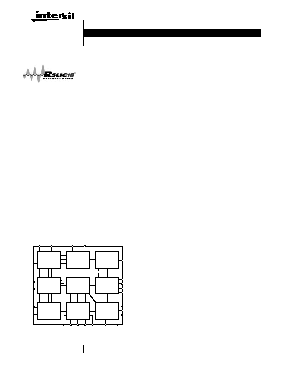
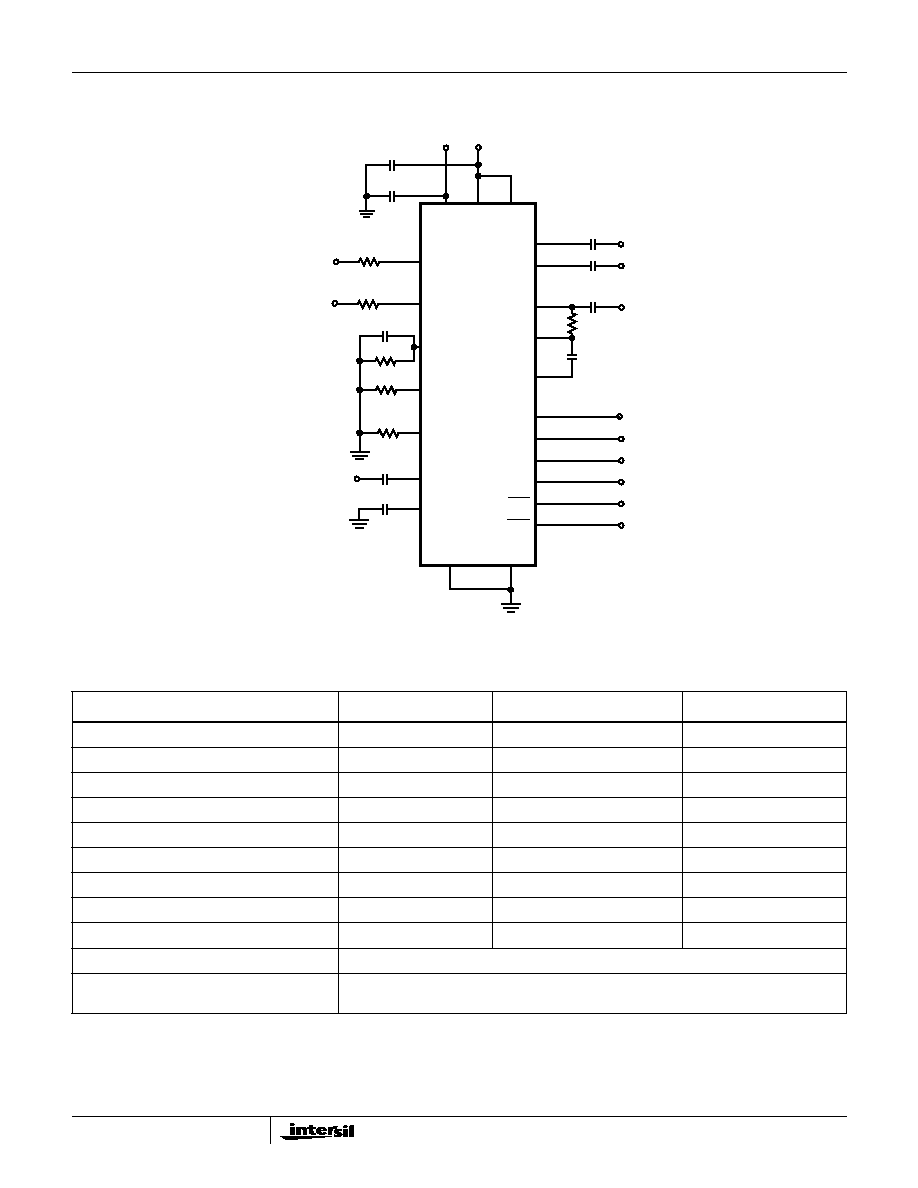
Block Diagram
Features
∑ Battery Operation to 100V
∑ Low Standby Power Consumption of 50mW
∑ Peak Ringing Amplitude 95V, 5 REN
∑ Sinusoidal or Trapezoidal Ringing Capability
∑ Integrated CODEC Ringing Interface
∑ Integrated MTU DC Characteristics
∑ Low External Component Count
∑ Pulse Metering and On Hook Transmission
∑ Tip Open Ground Start Operation
∑ Thermal Shutdown with Alarm Indicator
∑ 28 Lead Surface Mount Packaging
∑ Dielectric Isolated (DI) High Voltage Design
∑ HC55180
- Silent Polarity Reversal
- 53dB Longitudinal Balance
- Loopback Test Capability
∑ HC55181
- Integrated Battery Switch
- Silent Polarity Reversal
- 58/53dB Longitudinal Balance
- Loopback and Test Access Capability
∑ HC55182
- Integrated Battery Switch
- 58/53dB Longitudinal Balance
- Loopback and Test Access Capability
∑ HC55183
- Integrated Battery Switch
- 45dB Longitudinal Balance
∑ HC55184
- Integrated Battery Switch
- Silent Polarity Reversal
- 45dB Longitudinal Balance
Applications
∑ Wireless Local Loop (WLL)
∑ Digital Added Main Line (DAML)/Pairgain
∑ Integrated Services Digital Network (ISDN)
∑ Small Office Home Office (SOHO) PBX
∑ Cable/Computer Telephony
Related Literature
∑ AN9814, User's Guide for Development Board
∑ AN9824, Modeling of the AC Loop
∑ AN TBD, Interfacing to DSP CODECs
VRS
VRX
VTX
-IN
VFB
F2
F1
F0
ILIM
TIP
RING
SW+
SW-
RTD RD
DET ALM
RINGING
PORT
4-WIRE
PORT
CONTROL
LOGIC
BATTERY
SWITCH
TRANSMIT
SENSING
DETECTOR
LOGIC
DC
CONTROL
2-WIRE
PORT
TEST
ACCESS
E0
POL
CDC
VBH
VBL
BSEL
SWC
Data Sheet
October 1998
File Number
4519.4

29
Ordering Information (PLCC Package Only)
PART NUMBER
100V
85V
BAT
SW
POL
REV
FULL
TEST
LOOP
BACK
ONLY
LB = 53dB
LB = 58dB
TEMP.
RANGE
o
C
PACKAGE
PACKAGE
NO.
HC55180CIM
∑
∑
∑
∑
-40 to 85
28 Ld PLCC
N28.45
HC55180DIM
∑
∑
∑
∑
-40 to 85
28 Ld PLCC
N28.45
HC55181AIM
∑
∑
∑
∑
∑
-40 to 85
28 Ld PLCC
N28.45
HC55181BIM
∑
∑
∑
∑
∑
-40 to 85
28 Ld PLCC
N28.45
HC55181CIM
∑
∑
∑
∑
∑
-40 to 85
28 Ld PLCC
N28.45
HC55181DIM
∑
∑
∑
∑
∑
-40 to 85
28 Ld PLCC
N28.45
HC55182AIM
∑
∑
∑
∑
-40 to 85
28 Ld PLCC
N28.45
HC55182BIM
∑
∑
∑
∑
-40 to 85
28 Ld PLCC
N28.45
HC55182CIM
∑
∑
∑
∑
-40 to 85
28 Ld PLCC
N28.45
HC55182DIM
∑
∑
∑
∑
-40 to 85
28 Ld PLCC
N28.45
HC55183ECM
75V
∑
45dB
0 to 70
28 Ld PLCC
N28.45
HC55184ECM
75V
∑
∑
45dB
0 to 70
28 Ld PLCC
N28.45
HC5518XEVAL1
Evaluation board platform, including CODEC.
Device Operating Modes
OPERATING
MODE
F2
F1
F0
E0 = 1 E0 = 0
DESCRIPTION
HC55180
HC55181
HC55182
HC55183
HC55184
Low Power
Standby
0
0
0
SHD
GKD
MTU compliant standby
mode with active loop
detector.
∑
∑
∑
∑
∑
Forward Active
0
0
1
SHD
GKD
Forward battery loop feed.
∑
∑
∑
∑
∑
Unused
0
1
0
n/a
n/a
This is a reserved internal
test mode.
Reverse Active
0
1
1
SHD
GKD
Reverse battery loop feed.
∑
∑
∑
Ringing
1
0
0
RTD
RTD
Balanced ringing mode
supporting both sinusoidal,
trapezoidal and ringing
waveforms with DC offset.
∑
∑
∑
∑
∑
Forward Loop
Back
1
0
1
SHD
GKD
Internal device test mode.
∑
∑
∑
Tip Open
1
1
0
SHD
GKD
Tip amplifier disabled and
ring amplifier enabled.
Intended for PBX type
applications.
∑
∑
∑
Power Denial
1
1
1
n/a
n/a
Device shutdown.
∑
∑
∑
∑
∑
HC55180, HC55181, HC55182, HC55183, HC55184
30
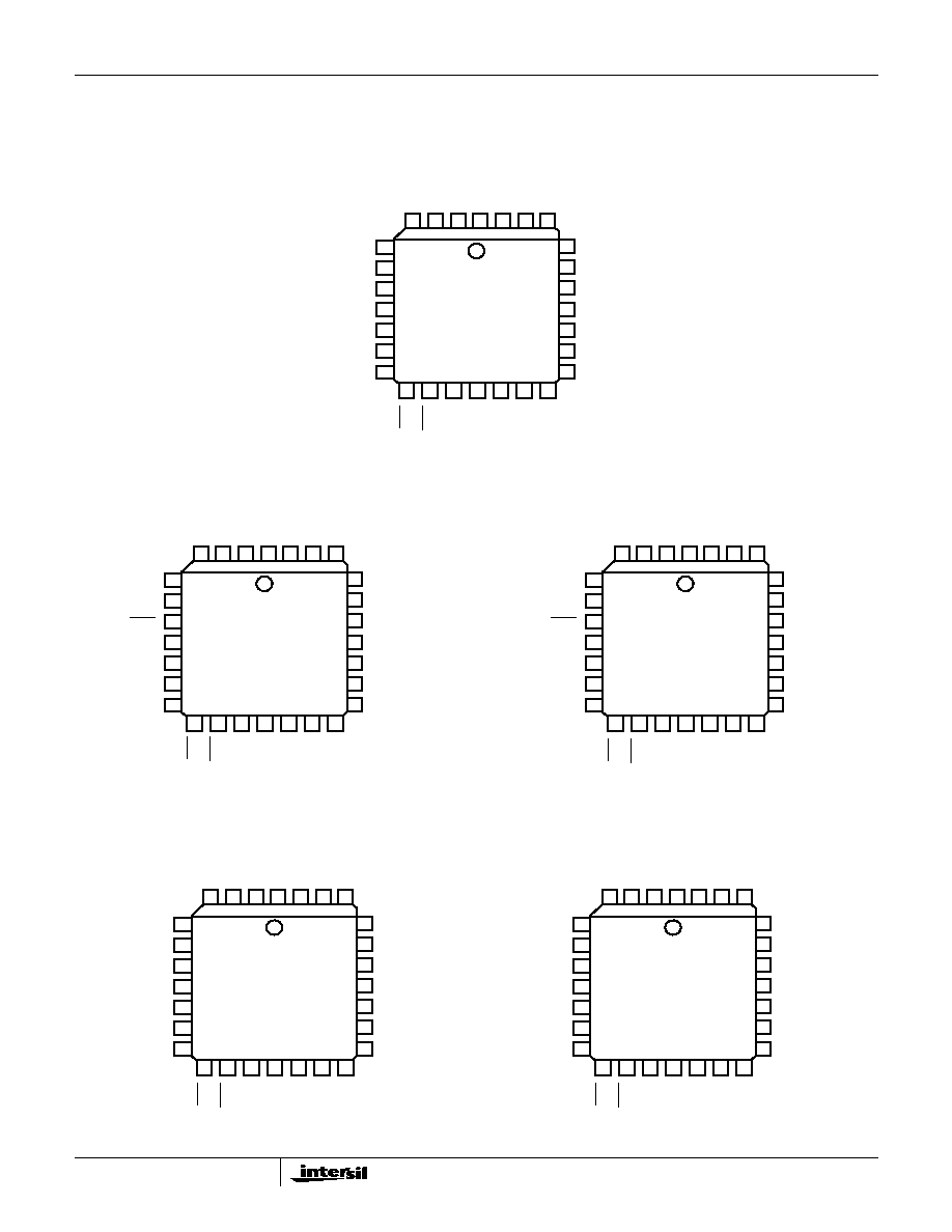
Pinouts
HC55180
(PLCC)
TOP VIEW
HC55181
(PLCC)
TOP VIEW
HC55182
(PLCC)
TOP VIEW
HC55183
(PLCC)
TOP VIEW
HC55184
(PLCC)
TOP VIEW
RING
ILIM
RTD
CDC
VRX
VRS
POL
NC
NC
RD
-IN
VFB
VCC
VTX
BGND
TIP
NC
E0
DET
ALM
A
GND
NC
VBL
VBH
NC
F2
F1
F0
5
6
7
8
9
10
11
12
13
14
15
16
17
18
1
2
3
4
19
20
21
22
23
24
25
26
27
28
RING
ILIM
RTD
CDC
VRX
VRS
POL
NC
BSEL
RD
-IN
VFB
VCC
VTX
BGND
TIP
SW-
E0
DET
ALM
A
GND
SW+
VBL
VBH
SWC
F2
F1
F0
5
6
7
8
9
10
11
12
13
14
15
16
17
18
1
2
3
4
19
20
21
22
23
24
25
26
27
28
RING
ILIM
RTD
CDC
VRX
VRS
NC
NC
BSEL
RD
-IN
VFB
VCC
VTX
BGND
TIP
SW-
E0
DET
ALM
A
GND
SW+
VBL
VBH
SWC
F2
F1
F0
5
6
7
8
9
10
11
12
13
14
15
16
17
18
1
2
3
4
19
20
21
22
23
24
25
26
27
28
RING
ILIM
RTD
CDC
VRX
VRS
NC
NC
BSEL
RD
-IN
VFB
VCC
VTX
BGND
TIP
NC
E0
DET
ALM
A
GND
NC
VBL
VBH
NC
F2
F1
F0
5
6
7
8
9
10
11
12
13
14
15
16
17
18
1
2
3
4
19
20
21
22
23
24
25
26
27
28
RING
ILIM
RTD
CDC
VRX
VRS
POL
NC
BSEL
RD
-IN
VFB
VCC
VTX
BGND
TIP
NC
E0
DET
ALM
A
GND
NC
VBL
VBH
NC
F2
F1
F0
5
6
7
8
9
10
11
12
13
14
15
16
17
18
1
2
3
4
19
20
21
22
23
24
25
26
27
28
HC55180, HC55181, HC55182, HC55183, HC55184

31
Absolute Maximum Ratings
T
A
= 25
o
C
Thermal Information
Maximum Supply Voltages
V
CC
. . . . . . . . . . . . . . . . . . . . . . . . . . . . . . . . . . . . . -0.5V to +7V
V
CC
- V
BAT
(180, 181, 182) . . . . . . . . . . . . . . . . . . . . . . . . . 110V
V
CC
- V
BAT
(183, 184) . . . . . . . . . . . . . . . . . . . . . . . . . . . . . . 85V
Uncommitted Switch Voltage . . . . . . . . . . . . . . . . . . . . . . . -110V
ESD (Human Body Model). . . . . . . . . . . . . . . . . . . . . . . . . . . . 500V
Operating Conditions
Temperature Range
Industrial (I suffix) . . . . . . . . . . . . . . . . . . . . . . . . . . -40
o
C to 85
o
C
Commercial (C suffix). . . . . . . . . . . . . . . . . . . . . . . . . 0
o
C to 75
o
C
Positive Power Supply (V
CC
) . . . . . . . . . . . . . . . . . . . . . . . +5V
±
5%
Negative Power Supply (V
BH
, V
BL
) (180, 181, 182) . -16V to -100V
Negative Power Supply (V
BH
, V
BL
) (183, 184) . . . . . . -24V to -75V
Uncommitted Switch (loop back or relay driver). . . . . . +5V to -100V
Thermal Resistance (Typical, Note 1)
JA
(
o
C/W)
PLCC Package . . . . . . . . . . . . . . . . . . . . . . . . . . . . .
53
Maximum Junction Temperature Plastic . . . . . . . . . . . . . . . . 150
o
C
Maximum Storage Temperature Range . . . . . . . . . . -65
o
C to 150
o
C
Maximum Lead Temperature (Soldering 10s) . . . . . . . . . . . . 300
o
C
(PLCC - Lead Tips Only)
Die Characteristics
Substrate Potential. . . . . . . . . . . . . . . . . . . . . . . . . . . . . . . . . . V
BAT
Process . . . . . . . . . . . . . . . . . . . . . . . . . . . . . . . . . . . . . . Bipolar-DI
CAUTION: Stresses above those listed in "Absolute Maximum Ratings" may cause permanent damage to the device. This is a stress only rating and operation of the
device at these or any other conditions above those indicated in the operational sections of this specification is not implied.
NOTE:
1.
JA
is measured with the component mounted on an evaluation PC board in free air.
Electrical Specifications
Unless Otherwise Specified, T
A
= 0
o
C to 70
o
C for the HC55183, 184 only, all others -40
o
C to 85
o
C, V
BL
= -24V,
V
BH
= -100V, -85V or -75V, V
CC
= +5V, AGND = BGND = 0V, loop current limit = 25mA. All AC Parameters are
specified at 600
2-wire terminating impedance over the frequency band of 300Hz to 3.4kHz. Protection
resistors = 0
. These parameters apply generically to each product offering.
PARAMETER
TEST CONDITIONS
MIN
TYP
MAX
UNITS
RINGING PARAMETERS (Note 2)
VRS Input Impedance (Note 3)
480
-
-
k
Differential Ringing Gain
VRS to 2-wire, R
LOAD
=
(Note 4)
78
80
82
V/V
4-Wire to 2-Wire Ringing Off Isolation
Active mode, referenced to VRS input.
-
60
-
dB
2-Wire to 4-Wire Transmit Isolation
Ringing mode referenced to the differential ringing
amplitude.
-
60
-
dB
AC TRANSMISSION PARAMETERS (Notes 5, 6)
Receive Input Impedance (Note 3)
160
-
-
k
Transmit Output Impedance (Note 3)
-
-
1
4-Wire Port Overload Level
THD = 1%
3.1
3.5
-
V
PK
2-Wire Port Overload Level
THD = 1%
3.1
3.5
-
V
PK
2-Wire Return Loss
300Hz
f
<
1kHz
30
45
-
dB
1kHz
f
3.4kHz
35
45
-
dB
Longitudinal Current Capability (Per Wire) (Note 3)
Test for False Detect
20
-
-
mA
RMS
Test for False Detect, Low Power Standby
10
-
-
mA
RMS
4-Wire to 2-Wire Insertion Loss
-0.20
0.0
+0.30
dB
2-Wire to 4-Wire Insertion Loss
-6.22
-6.02
-5.82
dB
4-Wire to 4-Wire Insertion Loss
-6.22
-6.02
-5.82
dB
Idle Channel Noise 2-Wire
C-Message
-
16
19
dBrnC
Psophometric
-
-73.5
-71
dBmp
Idle Channel Noise 4-Wire
C-Message
-
10
13
dBrnC
Psophometric
-
-79.5
-77
dBmp
DC PARAMETERS (Note 6)
Loop Current Limit Programming Range (Note 5)
Max Low Battery = -52V
15
-
45
mA
Loop Current During Low Power Standby
Forward polarity only.
18
-
26
mA
HC55180, HC55181, HC55182, HC55183, HC55184
32
NOTES:
2. These parameters are specified at high battery operation. For the HC55180 the external supply is set to high battery voltage, for the HC55181,
HC55182, HC55183 and HC55184, BSEL = 1.
3. These parameters are controlled via design or process parameters and are not directly tested. These parameters are characterized upon initial
design release and upon design changes which would affect these characteristics.
4. Differential Ringing Gain is measured with VRS = 0.795 V
RMS
for -100V devices, VRS = 0.663 V
RMS
for -85V devices and VRS = 0.575 V
RMS
for -75V devices.
5. These parameters are specified at low battery operation. For the HC55180, the external supply is set to low battery voltage, for the HC55181,
HC55182, HC55183 and HC55184, BSEL = 0.
6. Forward Active and Reverse Active performance is guaranteed for the HC55180, HC55181 and HC55184 devices only. The HC55182 and
HC55183 are specified for Forward Active operation only.
LOOP DETECTORS AND SUPERVISORY FUNCTIONS
Switch Hook Programming Range
5
-
15
mA
Switch Hook Programming Accuracy
Assumes 1% external programming resistor
-
2
10
%
Dial Pulse Distortion
-
-
1
%
Ring Trip Comparator Threshold
2.3
2.6
2.9
V
Ring Trip Programming Current Accuracy
-
-
10
%
Ground Key Threshold
10
12
13.5
mA
Thermal Alarm Output
IC junction temperature
-
175
-
o
C
LOGIC INPUTS (F0, F1, F2, E0, SWC)
Input Low Voltage
-
-
0.8
V
Input High Voltage
2.0
-
-
V
Input Low Current
V
IL
= 0.4V
-20
-
-
µ
A
Input High Current
V
IH
= 2.4V
-
-
5
µ
A
LOGIC OUTPUTS (DET, ALM)
Output Low Voltage
I
OL
= 5mA
-
-
0.4
V
Output High Voltage
I
OH
= 100
µ
A
2.4
-
-
V
POWER SUPPLY REJECTION RATIO
V
CC
to 2-Wire
f = 300Hz
-
40
-
dB
f = 1kHz
-
35
-
dB
f = 3.4kHz
-
28
-
dB
V
CC
to 4-Wire
f = 300Hz
-
45
-
dB
f = 1kHz
-
43
-
dB
f = 3.4kHz
-
33
-
dB
V
BL
to 2-Wire
300Hz
f
3.4kHz
-
30
-
dB
V
BL
to 4-Wire
300Hz
f
3.4kHz
-
35
-
dB
V
BH
to 2-Wire
300Hz
f
3.4kHz
-
33
-
dB
V
BH
to 4-Wire
300Hz
f
1kHz
-
40
-
dB
1kHz
<
f
3.4kHz
-
45
-
dB
Electrical Specifications
Unless Otherwise Specified, T
A
= 0
o
C to 70
o
C for the HC55183, 184 only, all others -40
o
C to 85
o
C, V
BL
= -24V,
V
BH
= -100V, -85V or -75V, V
CC
= +5V, AGND = BGND = 0V, loop current limit = 25mA. All AC Parameters are
specified at 600
2-wire terminating impedance over the frequency band of 300Hz to 3.4kHz. Protection
resistors = 0
. These parameters apply generically to each product offering. (Continued)
PARAMETER
TEST CONDITIONS
MIN
TYP
MAX
UNITS
HC55180, HC55181, HC55182, HC55183, HC55184
33
Electrical Specifications
Unless Otherwise Specified, T
A
= 0
o
C to 70
o
C for the HC55183, 184 only, all others -40
o
C to 85
o
C, V
BL
= -24V, V
CC
= +5V, AGND = BGND = 0V,
loop current limit = 25mA. All AC Parameters are specified at 600W 2-wire terminating impedance over the frequency band of 300Hz to 3.4kHz.
Protection resistors = 0W.
PARAMETER
HC55180 (Note 7)
HC55181, HC55182
HC55183, HC55184
UNITS
TEST CONDITIONS
MIN
TYP
MAX
TEST CONDITIONS
MIN
TYP
MAX
TEST CONDITIONS
MIN
TYP
MAX
RINGING PARAMETERS (Note 2)
Ringing Voltage
Open Circuit
(Note 8)
THD
0.5%
V
B
= -85V
-
80
-
THD
0.5%
V
BH
= -85V
80
-
-
THD
0.5%
V
BH
= -75V
70
-
-
V
PEAK
THD
0.5%
V
B
= -100V
-
95
-
THD
0.5%
V
BH
= -100V
95
-
-
(Note 9)
-
-
-
V
PEAK
Ringing Voltage
Load = 1.3K
(Notes 8, 10)
THD
2.5%
V
B
= -85V
-
80
-
THD
2.5%
V
BH
= -85V
80
-
-
THD
3.0%
V
BH
= -75V
70
-
-
V
PEAK
THD
2.0%
V
B
= -100V
-
95
-
THD
2.0%
V
BH
= -100V
95
-
-
(Note 9)
-
-
-
V
PEAK
Tip Centering Voltage
V
B
= -85V, R
L
=
-
2.5
-
V
BH
= -85V, R
L
=
-
-
2.5
V
BH
= -75V, R
L
=
-
-
3
V
V
B
= -100V, R
L
=
-
2.0
-
V
BH
= -100V, R
L
=
-
-
2.0
(Note 9)
-
-
-
V
Ring Centering Voltage
V
B
= -85V, R
L
=
-
2.5
-
V
BH
= -85V, R
L
=
-
-
2.5
V
BH
= -75V, R
L
=
-
-
3
V
V
B
= -100V, R
L
=
-
2.0
-
V
BH
= -100V, R
L
=
-
-
2.0
(Note 9)
-
-
-
V
AC TRANSMISSION PARAMETERS (Notes 5, 6)
2-Wire Longitudinal Balance
(Notes 12, 13)
(Note 11)
-
-
-
Grade A, B
58
62
-
Grade E
45
53
-
dB
Grade C, D
-
59
-
Grade C, D
53
59
-
(Note 11)
-
-
-
dB
4-Wire Longitudinal Balance
(Note 11)
-
-
-
Grade A, B
-
67
-
Grade E
-
58
-
dB
Grade C, D
-
64
-
Grade C, D
-
64
-
(Note 11)
-
-
-
dB
2-Wire to 4-Wire Level Linearity
4-Wire to 2-Wire Level
Linearity
Referenced to -10dBm
+3 to -40dBm, 1kHz
-
0.025
-
+3 to -40dBm, 1kHz
-
0.025
-
+3 to -40dBm, 1kHz
-
0.025
-
dB
-40 to -50dBm, 1kHz
-
0.050
-
-40 to -50dBm, 1kHz
-
0.050
-
-40 to -50dBm, 1kHz
-
0.050
-
dB
-50 to -55dBm, 1kHz
-
0.100
-
-50 to -55dBm, 1kHz
-
0.100
-
-50 to -55dBm, 1kHz
-
0.100
-
dB
DC PARAMETERS
Loop Current Accuracy
(Notes 5, 6)
I
L
= 25mA
-
7
-
I
L
= 25mA
-
-
7
I
L
= 25mA
-
-
10
%
Open Circuit Voltage
(|Tip - Ring|, Note 6)
V
B
= -16V
-
7.5
-
V
BL
= -16V
6.5
7.5
9.5
V
BL
= -16V
-
7.5
-
V
V
B
= -24V
14
15.5
17
V
BL
= -24V
14
15.5
17
V
BL
= -24V
14
15.5
17
V
V
B
= -85V
-
50
-
BSEL = 1, V
BH
= -85V
-
50
-
BSEL = 1, V
BH
= -75V
-
50
-
V
V
B
= -100V
-
50
-
BSEL = 1, V
BH
= -100V
-
50
-
(Note 9)
-
-
-
V
Low Power Standby
Open Circuit Voltage
(Tip - Ring, Note 2)
V
B
= -48V
43
45
47
V
BH
= -48V
43
45
47
V
BH
= -48V
43
45
47
V
V
B
= -85V
46
49
52
V
BH
= -85V
46
49
52
V
BH
= -75V
46
49
52
V
V
B
= -100V
46
49
52
V
BH
= -100V
46
49
52
(Note 9)
-
-
-
V
TEST ACCESS FUNCTIONS
Switch On Voltage
(Note 14)
-
-
-
I
OL
= 45mA
-
0.30
0.60
(Note 14)
-
-
-
V
Loopback Max Battery
-
-
52
-
-
52
(Note 15)
-
-
52
V
HC55180, HC55181, HC55182, HC55183, HC55184
34
HC55180, HC55181, HC55182, HC55183, HC55184
NOTES:
7. The HC55180 does not provide battery switch operation. Therefore all battery voltage ref-
erences will be made to V
B
. V
B
is the voltage applied to the common connection of the
device V
BL
and V
BH
pins. See the HC55180 Basic Application Circuit.
8. Ringing Voltage is measured with VRS = 0.839 V
RMS
for -100V devices, VRS = 0.707
V
RMS
for -85V devices and VRS = 0.619 V
RMS
for -75V devices.
9. The HC55183 and HC55184 devices are specified with a single high battery voltage grade.
10. The device represents a low output impedance during ringing. Therefore the voltage
across the ringing load is determined by the voltage divider formed by the protection resis-
tance, loop resistance and ringing load impedance.
11. The HC55180, HC55183 and HC55184 are specified with a single longitudinal balance grade.
12. Longitudinal Balance is tested per IEEE455-1985, with 368
per Tip and Ring Terminal.
13. These parameters are tested 100% at room temperature. These parameters are guaran-
teed not tested across temperature via statistical characterization.
14. The HC55180, HC55183 and HC55184 do not support uncommitted switch operation.
15. The HC55183 and HC55184 do not support the Forward Loopback operating mode.
16. The HC55183 and HC55184 do not support the Tip Open operating mode.
17. The power dissipation numbers are actual device measurements and will be less than
worse case calculations based on data sheet supply current limits.
SUPPLY CURRENTS (Supply currents not listed are considered negligible and do not contribute significantly to total power dissipation. All measurements made under open circuit load conditions.)
Low Power Standby
(Note 2)
I
CC
2.0
3.7
5.0
I
CC
2.0
3.7
5.0
I
CC
-
3.7
6.0
mA
I
B
, V
B
= -100V, -85V
-
0.375
0.600 I
BH
, V
BH
= -100V, -85V
-
0.375
0.600
I
BH
, V
BH
= -75V
-
0.375
-
mA
Forward or Reverse
(Note 5)
I
CC
2.5
4.0
5.0
I
CC
2.5
4.0
5.0
I
CC
2.0
4.0
6.0
mA
I
B
, V
B
= -24V
-
1.0
2.5
I
BL
-
1.0
2.5
I
BL
-
1.0
2.5
mA
Forward
(Note 2)
I
CC
3.5
5.5
7.0
I
CC
3.5
5.5
7.0
I
CC
2.0
5.5
8.0
mA
(Note 7)
-
-
-
I
BL
-
1.3
2.0
I
BL
-
1.3
2.5
mA
I
B
, V
B
= -100V, -85V
-
3.2
4.5
I
BH
, V
BH
= -100V, -85V
-
1.7
2.5
I
BH
, V
BH
= -75V
-
1.4
3.0
mA
Ringing
(Note 2)
I
CC
4.5
7.5
11
I
CC
4.5
7.5
11
I
CC
-
7.5
11
mA
(Note 7)
-
-
-
I
BL
-
0.4
7.5
I
BL
-
0.4
1.5
mA
I
B
, V
B
= -100V, -85V
-
2.3
5.0
I
BH
, V
BH
= -100V, -85V
-
1.3
2.5
I
BH
, V
BH
= -75V
-
1.3
2.5
mA
Forward Loopback
(Note 5)
I
CC
-
8.5
10.0
I
CC
-
8.5
10.0
(Note 15)
-
-
-
mA
I
B
, V
B
= -24V
-
19
23.5
I
BL
-
19
23.5
-
-
-
mA
Tip Open
(Note 5)
I
CC
-
-
5.5
I
CC
-
-
5.5
(Note 16)
-
-
-
mA
I
B
, V
B
= -24V
-
-
1.0
I
BL
-
-
1.0
-
-
-
mA
Power Denial
(Note 5)
I
CC
0.5
3.0
5.0
I
CC
0.5
3.0
4.5
I
CC
-
3.0
5.0
mA
I
B
, V
B
= -24V
-
0.2
0.5
I
BL
-
0.2
0.5
I
BL
-
0.2
0.5
mA
ON HOOK POWER DISSIPATION (Note 17)
Forward or Reverse
(Notes 5, 6)
V
B
= -24V
-
44
60
V
BL
= -24V
-
44
60
V
BL
= -24V
-
44
60
mW
Low Power Standby
(Note 2)
V
B
= -85V
-
52
-
V
BH
= -85V
-
52
65
V
BH
= -75V
-
46
65
mW
V
B
= -100V
-
59
-
V
BH
= -100V
-
59
75
(Note 9)
Ringing
(Note 2)
V
B
= -85V
-
190
-
V
BH
= -85V
-
190
275
V
BH
= -75V
-
170
250
mW
V
B
= -100V
-
220
-
V
BH
= -100V
-
220
300
(Note 9)
OFF HOOK POWER DISSIPATION (Notes 5, 17)
Forward or Reverse
V
B
= -24V
-
290
-
V
BL
= -24V
-
290
310
V
BL
= -24V
-
280
310
mW
Electrical Specifications
Unless Otherwise Specified, T
A
= 0
o
C to 70
o
C for the HC55183, 184 only, all others -40
o
C to 85
o
C, V
BL
= -24V, V
CC
= +5V, AGND = BGND = 0V,
loop current limit = 25mA. All AC Parameters are specified at 600W 2-wire terminating impedance over the frequency band of 300Hz to 3.4kHz.
Protection resistors = 0W. (Continued)
PARAMETER
HC55180 (Note 7)
HC55181, HC55182
HC55183, HC55184
UNITS
TEST CONDITIONS
MIN
TYP
MAX
TEST CONDITIONS
MIN
TYP
MAX
TEST CONDITIONS
MIN
TYP
MAX
35
Design Equations
Loop Supervision Thresholds
SWITCH HOOK DETECT
The switch hook detect threshold is set by a single external
resistor, R
SH
. Equation 1 is used to calculate the value of R
SH
.
The term I
SH
is the desired DC loop current threshold. The
loop current threshold programming range is from 5mA to
15mA.
GROUND KEY DETECT
The ground key detector senses a DC current imbalance
between the Tip and Ring terminals when the ring terminal is
connected to ground. The ground key detect threshold is not
externally programmable and is internally fixed to 12mA
regardless of the switch hook threshold.
RING TRIP DETECT
The ring trip detect threshold is set by a single external
resistor, R
RT
. I
RT
should be set between the peak ringing
current and the peak off hook current while still ringing.
The capacitor C
RT
, in parallel with R
RT
, will set the ring trip
response time.
Loop Current Limit
The loop current limit of the device is programmed by the
external resistor R
IL
. The value of R
IL
can be calculated
using Equation 3.
The term I
LIM
is the desired loop current limit. The loop
current limit programming range is from 15mA to 45mA.
Impedance Matching
The impedance of the device is programmed with the
external component R
S
. R
S
is the gain setting resistor for
the feedback amplifier that provides impedance matching. If
complex impedance matching is required, then a complex
network can be substituted for R
S
.
RESISTIVE IMPEDANCE SYNTHESIS
The source impedance of the device, Z
O
, can be calculated
in Equation 4.
The required impedance is defined by the terminating
impedance and protection resistors as shown in Equation 5.
4-WIRE TO 2-WIRE GAIN
The 4-wire to 2-wire gain is defined as the receive gain. It is
a function of the terminating impedance, synthesized
impedance and protection resistors. Equation 6 calculates
the receive gain, G
42
.
When the device source impedance and protection resistors
equals the terminating impedance, the receive gain equals
unity.
2-WIRE TO 4-WIRE GAIN
The 2-wire to 4-wire gain (G
24
) is the gain from tip and ring to
the VTX output. The transmit gain is calculated in Equation 7.
When the protection resistors are set to zero, the transmit
gain is -6dB.
TRANSHYBRID GAIN
The transhybrid gain is defined as the 4-wire to 4-wire gain
(G
44
).
When the protection resistors are set to zero, the transhybrid
gain is -6dB.
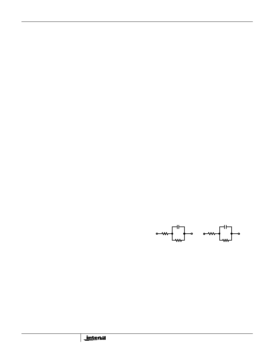
COMPLEX IMPEDANCE SYNTHESIS
Substituting the impedance programming resistor, R
S
, with a
complex programming network provides complex
impedance synthesis.
The reference designators in the programming network
match the evaluation board. The component R
S
has a
different design equation than the R
S
used for resistive
impedance synthesis. The design equations for each
component are provided below.
R
SH
600 I
SH
/
=
(EQ. 1)
R
RT
1800 I
RT
/
=
(EQ. 2)
R
IL
1760
I
LIM
-------------
=
(EQ. 3)
R
S
400 Z
O
(
)
=
(EQ. 4)
Z
O
Z
L
2R
P
≠
=
(EQ. 5)
G
42
2
Z
L
Z
O
+ 2R
P
+ Z
L
------------------------------------------
≠
=
(EQ. 6)
G
24
Z
O
Z
O
+ 2R
P
+ Z
L
------------------------------------------
≠
=
(EQ. 7)
G
44
Z
O
Z
O
2R
P
Z
L
+
+
---------------------------------------
≠
=
(EQ. 8)
FIGURE 1. COMPLEX PROGRAMMING NETWORK
2-WIRE
NETWORK
R
1
R
2
C
2
PROGRAMMING
NETWORK
R
S
R
P
C
P
R
S
400
R
1
2 R
P
(
)
≠
(
)
◊
=
(EQ. 9)
R
P
400
R
2
◊
=
(EQ. 10)
C
P
C
2
400
/
=
(EQ. 11)
HC55180, HC55181, HC55182, HC55183, HC55184
36
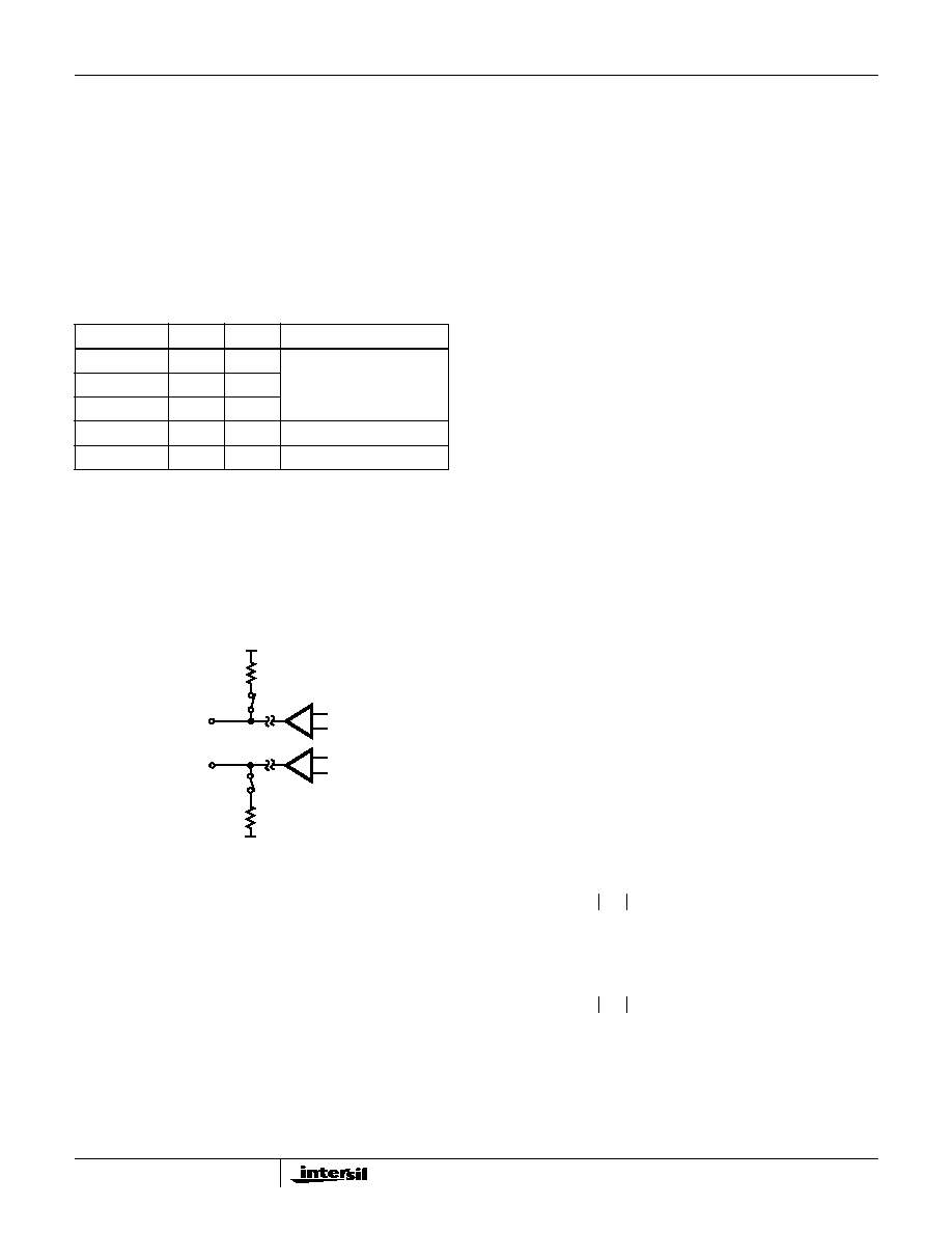
Low Power Standby
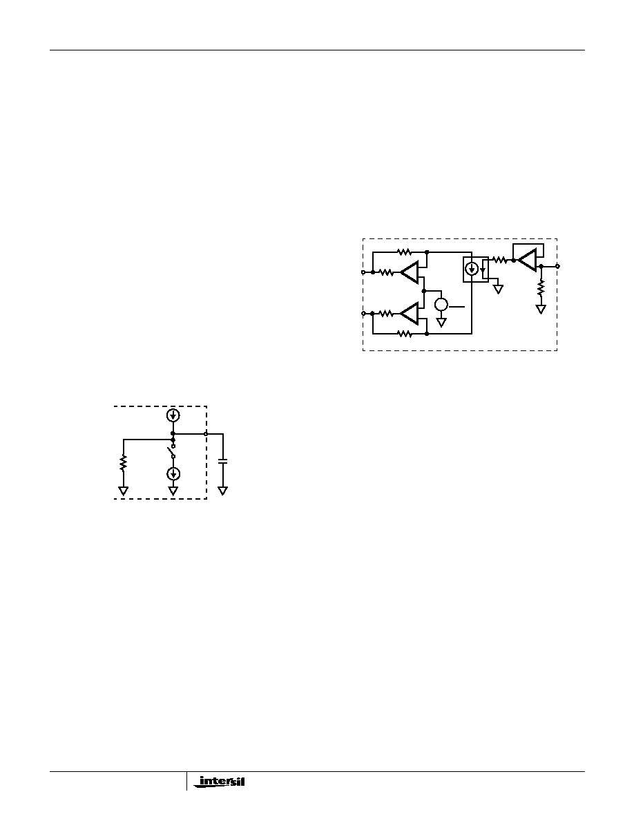
Overview
The low power standby mode (LPS, 000) should be used
during idle line conditions. The device is designed to operate
from the high battery during this mode. Most of the internal
circuitry is powered down, resulting in low power dissipation.
If the 2-wire (tip/ring) DC voltage requirements are not
critical during idle line conditions, the device may be
operated from the low battery. Operation from the low
battery will decrease the standby power dissipation.
2-Wire Interface
During LPS, the 2-wire interface is maintained with internal
switches and voltage references. The Tip and Ring
amplifiers are turned off to conserve power. The device will
provide MTU compliance, loop current and loop supervision.
Figure 2 represents the internal circuitry providing the 2-wire
interface during low power standby.
MTU Compliance
Maintenance Termination Unit or MTU compliance places
DC voltage requirements on the 2-wire terminals during idle
line conditions. The minimum idle voltage is 42.75V. The
high side of the MTU range is 56V. The voltage is expressed
as the difference between Tip and Ring.
The Tip voltage is held near ground through a 600
resistor
and switch. The Ring voltage is limited to a maximum of
-49V (by MTU REF) when operating from either the high or
low battery. A switch and 600
resistor connect the MTU
reference to the Ring terminal. When the high battery
voltage exceeds the MTU reference of -49V (typically), the
Ring terminal will be clamped by the internal reference. The
same Ring relationships apply when operating from the low
battery voltage. For high battery voltages (VBH) less than or
equal to the internal MTU reference threshold:
Loop Current
During LPS, the device will provide current to a load. The
current path is through resistors and switches, and will be
function of the off hook loop resistance (R
LOOP
). This
includes the off hook phone resistance and copper loop
resistance. The current available during LPS is determined
by Equation 13.
Internal current limiting of the standby switches will limit the
maximum current to 20mA.
Another loop current related parameter is longitudinal
current capability. The longitudinal current capability is
reduced to 10mA
RMS
per pin. The reduction in longitudinal
current capability is a result of turning off the Tip and Ring
amplifiers.
On Hook Power Dissipation
The on hook power dissipation of the device during LPS is
determined by the operating voltages and quiescent currents
and is calculated using Equation 14.
The quiescent current terms are specified in the electrical
tables for each operating mode. Load power dissipation is
not a factor since this is an on hook mode. Some
applications may specify a standby current. The standby
current may be a charging current required for modern
telephone electronics.
Standby Current Power dissipation
Any standby line current, I
SLC
, introduces an additional
power dissipation term P
SLC
. Equation 15 illustrates the
power contribution is zero when the standby line current is
zero.
If the battery voltage is less than -49V (the MTU clamp is
off), the standby line current power contribution reduces to
Equation 16.
Most applications do not specify charging current
requirements during standby. When specified, the typical
charging current may be as high as 5mA.
TABLE 1. DEVICE INTERFACES DURING LPS
INTERFACE
ON
OFF
NOTES
Receive
x
AC transmission, impedance
matching and ringing are dis-
abled during this mode.
Ringing
x
Transmit
x
2-Wire
x
Amplifiers disabled.
Loop Detect
x
Switch hook or ground key.
FIGURE 2. LPS 2-WIRE INTERFACE CIRCUIT DIAGRAM
TIP AMP
RING AMP
TIP
RING
MTU REF
GND
600
600
V
RING
V
BH
4
+
=
(EQ. 12)
I
LOOP
1
≠
49
≠
(
)
≠
(
)
600
600
R
LOOP
+
+
(
)
/
=
(EQ. 13)
P
LPS
V
BH
I
BHQ
◊
V
BL
I
BLQ
◊
V
CC
I
CCQ
◊
+
+
=
(EQ. 14)
P
SLC
I
SLC
V
BH
49
≠
1
I
SLC
x1200
+
+
(
)
◊
=
(EQ. 15)
P
SLC
I
SLC
V
BH
1
I
SLC
x1200
+
+
(
)
◊
=
(EQ. 16)
HC55180, HC55181, HC55182, HC55183, HC55184
37
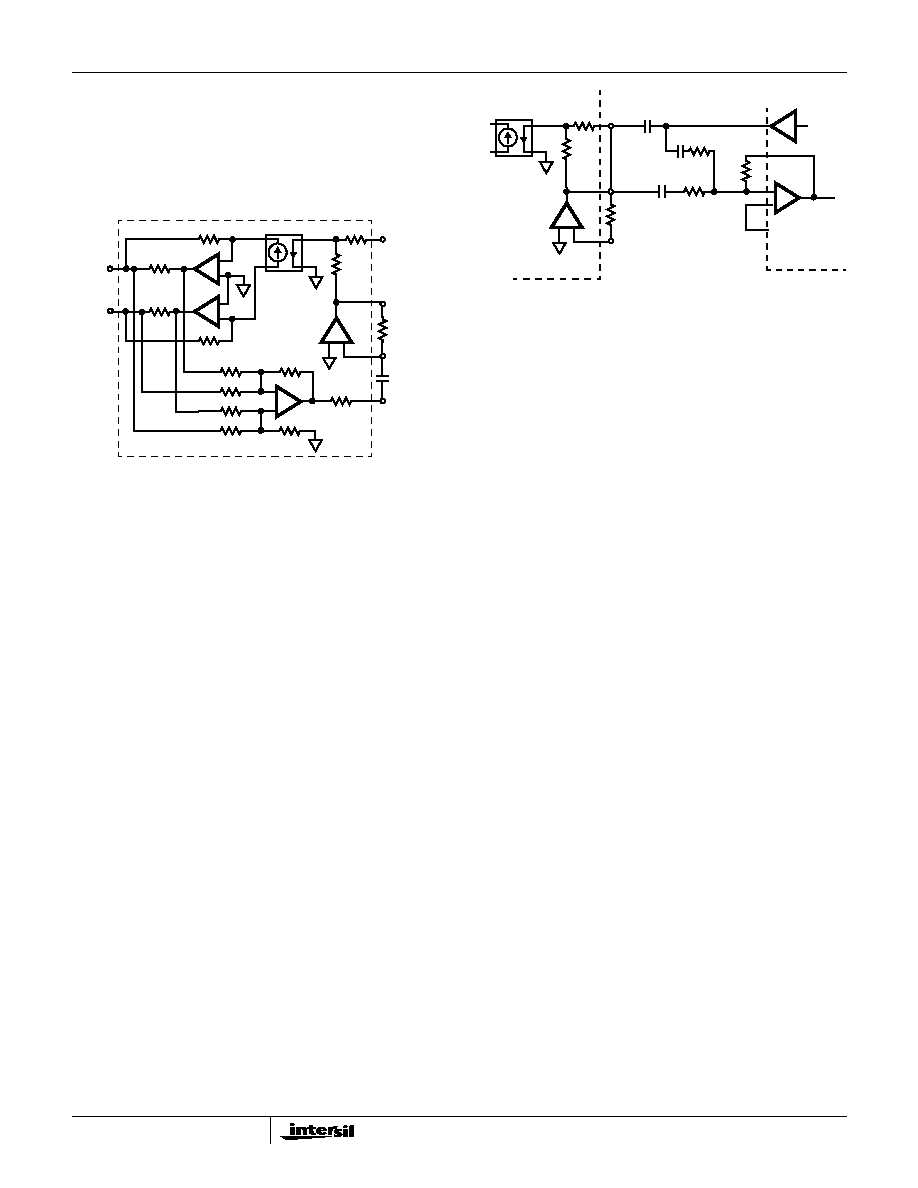
Forward Active
Overview
The forward active mode (FA, 001) is the primary AC
transmission mode of the device. On hook transmission, DC
loop feed and voice transmission are supported during forward
active. Loop supervision is provided by either the switch hook
detector (E0 = 1) or the ground key detector (E0 = 0). The
device may be operated from either high or low battery for on-
hook transmission and low battery for loop feed.
On-Hook Transmission
The primary purpose of on hook transmission will be to
support caller ID and other advanced signalling features.
The transmission over load level while on hook is 3.5V
PEAK
.
When operating from the high battery, the DC voltages at Tip
and Ring are MTU compliant. The typical Tip voltage is -4V
and the Ring voltage is a function of the battery voltage for
battery voltages less than -60V as shown in Equation 17.
Loop supervision is provided by the switch hook detector at
the DET output. When DET goes low, the low battery should
be selected for DC loop feed and voice transmission.
Feed Architecture
The design implements a voltage feed current sense
architecture. The device controls the voltage across Tip and
Ring based on the sensing of load current. Resistors are
placed in series with Tip and Ring outputs to provide the
current sensing. The diagram below illustrates the concept.
By monitoring the current at the amplifier output, a negative
feedback mechanism sets the output voltage for a defined
load. The amplifier gains are set by resistor ratios (R
A
, R
B
,
R
C
) providing all the performance benefits of matched
resistors. The internal sense resistor, R
CS
, is much smaller
than the gain resistors and is typically 20
for this device.
The feedback mechanism, K
S
, represents the amplifier
configuration providing the negative feedback.
DC Loop Feed
The feedback mechanism for monitoring the DC portion of
the loop current is the loop detector. A low pass filter is used
in the feedback to block voice band signals from interfering
with the loop current limit function. The pole of the low pass
filter is set by the external capacitor C
DC
. The value of the
external capacitor should be 4.7
µ
F.
Most applications will operate the device from low battery
while off hook. The DC feed characteristic of the device will
drive Tip and Ring towards half battery to regulate the DC
loop current. For light loads, Tip will be near -4V and Ring
will be near V
VBL
+ 4V. The following diagram shows the DC
feed characteristic.
The point on the y-axis labeled V
TR(OC)
is the open circuit
Tip to Ring voltage and is defined by the feed battery
voltage.
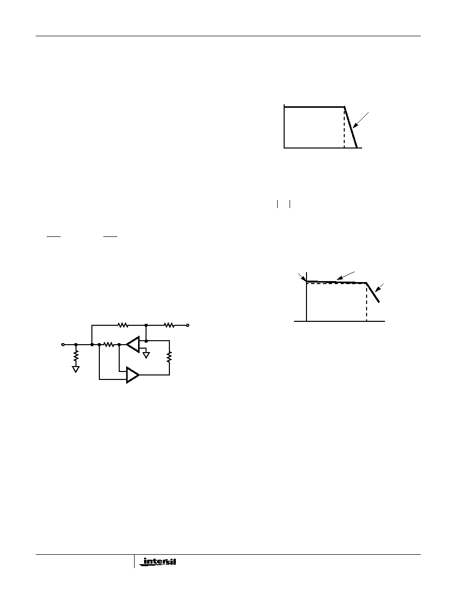
The curve of Figure 5 determines the actual loop current for
a given set of loop conditions. The loop conditions are
determined by the low battery voltage and the DC loop
impedance. The DC loop impedance is the sum of the
protection resistance, copper resistance (ohms/foot) and the
telephone off hook DC resistance.
The slope of the feed characteristic and the battery voltage
define the maximum loop current on the shortest possible
loop as the short circuit current I
SC
.
The term I
LIM
is the programmed current limit, 1760/R
IL
.
The line segment I
A
represents the constant current region
of the loop current limit function.
The maximum loop impedance for a programmed loop
current is defined as R
KNEE
.
When R
KNEE
is exceeded, the device will transition from
constant current feed to constant voltage, resistive feed. The
line segment I
B
represents the resistive feed portion of the
load characteristic.
V
RING
V
BH
4
+
=
(EQ. 17)
FIGURE 3. VOLTAGE FEED CURRENT SENSE DIAGRAM
+
-
+
-
V
IN
V
OUT
R
C
R
CS
R
L
R
B
R
A
K
S
FIGURE 4. DC FEED CHARACTERISTIC
m = (
V
TR
/
I
L
) = 10k
I
LOOP
(mA)
I
LIM
V
TR(OC)
V
TR
, DC (V)
V
TR OC
(
)
V
BL
8
≠
=
(EQ. 18)
FIGURE 5. I
LOOP
VERSUS R
LOOP
LOAD CHARACTERISTIC
R
LOOP
(
)
R
KNEE
I
LIM
I
LOOP
(mA)
I
SC
I
A
I
B
2R
P
I
SC
I
LIM
V
TR OC
(
)
2R
P
I
LIM
≠
10e3
------------------------------------------------------
+
=
(EQ. 19)
I
A
I
LIM
V
TR OC
(
)
R
LOOP
I
LIM
≠
10e3
--------------------------------------------------------------
+
=
(EQ. 20)
R
KNEE
V
TR OC
(
)
I
LIM
------------------------
=
(EQ. 21)
I
B
V
TR OC
(
)
R
LOOP
------------------------
=
(EQ. 22)
HC55180, HC55181, HC55182, HC55183, HC55184
38
Voice Transmission
The feedback mechanism for monitoring the AC portion of
the loop current consists of two amplifiers, the sense
amplifier (SA) and the transmit amplifier (TA). The AC
feedback signal is used for impedance synthesis. A detailed
model of the AC feed back loop is provided below.
The gain of the transmit amplifier, set by R
S
, determines the
programmed impedance of the device. The capacitor C
FB
blocks the DC component of the loop current. The ground
symbols in the model represent AC grounds, not actual DC
potentials.
The sense amp output voltage, V
SA
, as a function of Tip and
Ring voltage and load is calculated using Equation 23.
The transmit amplifier provides the programmable gain
required for impedance synthesis. In addition, the output of
this amplifier interfaces to the CODEC transmit input. The
output voltage is calculated using Equation 24.
Once the impedance matching components have been
selected using the design equations, the above equations
provide additional insight as to the expected AC node
voltages for a specific Tip and Ring load.
Transhybrid Balance
The final step in completing the impedance synthesis design
is calculating the necessary gains for transhybrid balance.
The AC feed back loop produces an echo at the V
TX
output
of the signal injected at V
RX
. The echo must be cancelled to
maintain voice quality. Most applications will use a summing
amplifier in the CODEC front end as shown below to cancel
the echo signal.
The resistor ratio, R
F
/R
B
, provides the final adjustment for
the transmit gain, G
TX
. The transmit gain is calculated using
Equation 25.
Most applications set R
F
= R
B
, hence the device 2-wire to
4-wire equals the transmit gain. Typically R
B
is greater than
20k
to prevent loading of the device transmit output.
The resistor ratio, R
F
/R
A
, is determined by the transhybrid
gain of the device, G
44
. R
F
is previously defined by the
transmit gain requirement and R
A
is calculated using
Equation 26.
Power Dissipation
The power dissipated by the device during on hook
transmission is strictly a function of the quiescent currents
for each supply voltage during Forward Active operation.
Off hook power dissipation is increased above the quiescent
power dissipation by the DC load. If the loop length is less
than or equal to R
KNEE
, the device is providing constant
current, I
A
, and the power dissipation is calculated using
Equation 28.
If the loop length is greater than R
KNEE
, the device is operating
in the constant voltage, resistive feed region. The power
dissipated in this region is calculated using Equation 29.
Since the current relationships are different for constant
current versus constant voltage, the region of device
operation is critical to valid power dissipation calculations.
FIGURE 6. AC SIGNAL TRANSMISSION MODEL
TIP
RING
+
-
-IN
VFB
VRX
VTX
R
R
R
R
+
-
+
-
+
-
1:1
20
20
0.75R
3R
3R
3R
3R
R/2
8K
R
S
C
FB
T
A
V
SA
V
SA
V
T
V
R
≠
(
)
≠
10
Z
L
------
=
(EQ. 23)
V
VTX
V
SA
R
S
8e3
----------
≠
=
(EQ. 24)
FIGURE 7. TRANSHYBRID BALANCE INTERFACE
+
-
R
F
R
B
R
A
HC5518x
CODEC
+2.4V
RX OUT
TX IN
-IN
VRX
VTX
R
R
+
-
1:1
R
S
T
A
G
TX
G
≠
24
R
F
R
B
--------
=
(EQ. 25)
R
A
R
B
G
44
----------
=
(EQ. 26)
P
FAQ
V
BH
I
◊
BHQ
V
BL
I
BLQ
◊
V
CC
I
CCQ
◊
+
+
=
(EQ. 27)
P
FA IA
( )
P
FA Q
( )
V
BL
xI
A
(
)
R
LOOP
xI
2
A
(
)
≠
+
=
(EQ. 28)
P
FA IB
( )
P
FA Q
( )
V
BL
xI
B
(
)
R
LOOP
xI
2
B
(
)
≠
+
=
(EQ. 29)
HC55180, HC55181, HC55182, HC55183, HC55184
39
Reverse Active
Overview
The reverse active mode (RA, 011) provides the same
functionality as the forward active mode. On hook
transmission, DC loop feed and voice transmission are
supported. Loop supervision is provided by either the switch
hook detector (E0 = 1) or the ground key detector (E0 = 0).
The device may be operated from either high or low battery.
During reverse active the Tip and Ring DC voltage
characteristics exchange roles. That is, Ring is typically 4V
below ground and Tip is typically 4V more positive than
battery. Otherwise, all feed and voice transmission
characteristics are identical to forward active.
Silent Polarity Reversal
Changing from forward active to reverse active or vice versa
is referred to as polarity reversal. Many applications require
slew rate control of the polarity reversal event. Requirements
range from minimizing cross talk to protocol signalling.
The device uses an external low voltage capacitor, C
POL
, to
set the reversal time. Once programmed, the reversal time
will remain nearly constant over various load conditions. In
addition, the reversal timing capacitor is isolated from the AC
loop, therefore loop stability is not impacted.
The internal circuitry used to set the polarity reversal time is
shown below.
During forward active, the current from source I1 charges the
external timing capacitor C
POL
and the switch is open. The
internal resistor provides a clamping function for voltages on
the POL node. During reverse active, the switch closes and
I2 (roughly twice I1) pulls current from I1 and the timing
capacitor. The current at the POL node provides the drive to
a differential pair which controls the reversal time of the Tip
and Ring DC voltages.
Where
time is the required reversal time. Polarized
capacitors may be used for C
POL
. The low voltage at the
POL pin and minimal voltage excursion
±
0.75V, are well
suited to polarized capacitors.
Power Dissipation
The power dissipation equations for forward active operation
also apply to the reverse active mode.
Ringing
Overview
The ringing mode (RNG, 100) provides linear amplification
to support a variety of ringing waveforms. A programmable
ring trip function provides loop supervision and auto
disconnect upon ring trip. The device is designed to operate
from the high battery during this mode.
Architecture
The device provides linear amplification to the signal applied
to the ringing input, V
RS
. The differential ringing gain of the
device is 80V/V. The circuit model for the ringing path is
shown in the following figure.
The voltage gain from the VRS input to the Tip output is
40V/V. The resistor ratio provides a gain of 8 and the current
mirror provides a gain of 5. The voltage gain from the VRS
input to the Ring output is -40V/V. The equations for the Tip
and Ring outputs during ringing are provided below.
When the input signal at VRS is zero, the Tip and Ring
amplifier outputs are centered at half battery. The device
provides auto centering for easy implementation of
sinusoidal ringing waveforms. Both AC and DC control of the
Tip and Ring outputs is available during ringing. This feature
allows for DC offsets as part of the ringing waveform.
Ringing Input
The ringing input, V
RS
, is a high impedance input. The high
impedance allows the use of low value capacitors for AC
coupling the ring signal. The V
RS
input is enabled only
during the ringing mode, therefore a free running oscillator
may be connected to VRS at all times.
When operating from a battery of -100V, each amplifier, Tip
and Ring, will swing a maximum of 95V
P-P
. Hence, the
maximum signal swing at VRS to achieve full scale ringing is
approximately 2.4V
P-P
. The low signal levels are compatible
with the output voltage range of the CODEC. The digital
nature of the CODEC ideally suits it for the function of
programmable ringing generator. See Applications.
FIGURE 8. REVERSAL TIMING CONTROL
C
POL
POL
I
1
75k
I
2
C
POL
time
75000
----------------
=
(EQ. 30)
FIGURE 9. LINEAR RINGING MODEL
TIP
RING
VRS
R/8
R
R
+
-
+
-
5:1
20
20
+
-
+
-
800K
V
BH
2
V
T
V
BH
2
-----------
40
VRS
◊
(
)
+
=
(EQ. 31)
V
R
V
BH
2
-----------
40
VRS
◊
(
)
≠
=
(EQ. 32)
HC55180, HC55181, HC55182, HC55183, HC55184
40
Logic Control
Ringing patterns consist of silent intervals. The ringing to
silent pattern is called the ringing cadence. During the silent
portion of ringing, the device can be programmed to any
other operating mode. The most likely candidates are low
power standby or forward active. Depending on system
requirements, the low or high battery may be selected.
Loop supervision is provided with the ring trip detector. The ring
trip detector senses the change in loop current when the phone
is taken off hook. The loop detector full wave rectifies the
ringing current, which is then filtered with external components
R
RT
and C
RT
. The resistor R
RT
sets the trip threshold and the
capacitor C
RT
sets the trip response time. Most applications will
require a trip response time less than 150ms.
Three very distinct actions occur when the devices detects a
ring trip. First, the DET output is latched low. The latching
mechanism eliminates the need for software filtering of the
detector output. The latch is cleared when the operating
mode is changed externally. Second, the VRS input is
disabled, removing the ring signal from the line. Third, the
device is internally forced to the forward active mode.
Power Dissipation
The power dissipation during ringing is dictated by the load
driving requirements and the ringing waveform. The key to valid
power calculations is the correct definition of average and RMS
currents. The average current defines the high battery supply
current. The RMS current defines the load current.
The cadence provides a time averaging reduction in the
peak power. The total power dissipation consists of ringing
power, P
r
, and the silent interval power, P
s
.
The terms t
R
and t
S
represent the cadence. The ringing
interval is t
R
and the silent interval is t
S
. The typical cadence
ratio t
R
:t
S
is 1:2.
The quiescent power of the device in the ringing mode is
defined in Equation 34.
The total power during the ringing interval is the sum of the
quiescent power and loading power:
For sinusoidal waveforms, the average current, I
AVG
, is
defined in Equation 36.
The silent interval power dissipation will be determined by
the quiescent power of the selected operating mode.
Forward Loop Back
Overview
The forward loop back mode (FLB, 101) provides test
capability for the device. An internal signal path is enabled
allowing for both DC and AC verification. The internal 600
terminating resistor has a tolerance of
±
20%. The device is
intended to operate from only the low battery during this
mode.
Architecture
When the forward loop back mode is initiated internal
switches connect a 600
load across the outputs of the Tip
and Ring amplifiers.
DC Verification
When the internal signal path is provided, DC current will
flow from Tip to Ring. The DC current will force DET low,
indicating the presence of loop current. In addition, the ALM
output will also go low. This does not indicate a thermal
alarm condition. Rather, proper logic operation is verified in
the event of a thermal shutdown. In addition to verifying
device functionality, toggling the logic outputs verifies the
interface to the system controller.
AC Verification
The entire AC loop of the device is active during the forward
loop back mode. Therefore a 4-wire to 4-wire level test
capability is provided. Depending on the transhybrid balance
implementation, test coverage is provided by a one or two
step process.
System architectures which cannot disable the transhybrid
function would require a two step process. The first step
would be to send a test tone to the device while on hook and
not in forward loop back mode. The return signal would be
the test level times the gain R
F
/R
A
of the transhybrid
amplifier. Since the device would not be terminated,
cancellation would not occur. The second step would be to
program the device to FLB and resend the test tone. The
return signal would be much lower in amplitude than the first
step, indicating the device was active and the internal
termination attenuated the return signal.
System architectures which disable the transhybrid function
would achieve test coverage with a signal step. Once the
transhybrid function is disable, program the device for FLB
and send the test tone. The return signal level is determined
by the 4-wire to 4-wire gain of the device.
P
RNG
P
r
t
r
t
r
t
s
+
--------------
◊
P
s
t
s
t
r
t
s
+
--------------
◊
+
=
(EQ. 33)
P
r Q
( )
V
BH
I
BHQ
◊
V
BL
I
BLQ
◊
V
CC
I
CCQ
◊
+
+
=
(EQ. 34)
P
r
P
r Q
( )
V
BH
I
AVG
◊
V
RMS
2
Z
REN
R
LOOP
+
------------------------------------------
≠
+
=
(EQ. 35)
I
AVG
2
---
V
RMS
2
◊
Z
REN
R
LOOP
+
------------------------------------------
=
(EQ. 36)
FIGURE 10. FORWARD LOOP BACK INTERNAL TERMINATION
RING AMP
TIP AMP
RING
TIP
600
HC55180, HC55181, HC55182, HC55183, HC55184
41
Tip Open
Overview
The tip open mode (110) is intended for compatibility for
PBX type interfaces. Used during idle line conditions, the
device does not provide transmission. Loop supervision is
provided by either the switch hook detector (E0 = 1) or the
ground key detector (E0 = 0). The ground key detector will
be used in most applications. The device may be operated
from either high or low battery.
Functionality
During tip open operation, the Tip amplifier is disabled and
the Ring amplifier is enabled. The minimum Tip impedance
is 30k
. The only active path through the device will be the
Ring amplifier.
In keeping with the MTU characteristics of the device, Ring
will not exceed -56.5V when operating from the high battery.
Though MTU does not apply to tip open, safety requirements
are satisfied.
On Hook Power Dissipation
The on hook power dissipation of the device during tip open
is determined by the operating voltages and quiescent
currents and is calculated using Equation 37.
The quiescent current terms are specified in the electrical
tables for each operating mode. Load power dissipation is
not a factor since this is an on hook mode.
Power Denial
Overview
The power denial mode (111) will shutdown the entire device
except for the logic interface. Loop supervision is not
provided. This mode may be used as a sleep mode or to
shut down in the presence of a persistent thermal alarm.
Switching between high and low battery will have no effect
during power denial.
Functionality
During power denial, both the Tip and Ring amplifiers are
disabled, representing high impedances. The voltages at
both outputs are near ground.
Thermal Shutdown
In the event the safe die temperature is exceeded, the ALM
output will go low and DET will go high and the part will
automatically shut down. When the device cools, ALM will
go high and DET will reflect the loop status. If the thermal
fault persists, ALM will go low again and the part will shut
down. Programming power denial will permanently
shutdown the device and stop the self cooling cycling.
Battery Switching
Overview
The integrated battery switch selects between the high
battery and low battery. The battery switch is controlled
with the logic input BSEL. When BSEL is a logic high, the
high battery is selected and when a logic low, the low
battery is selected. All operating modes of the device will
operate from high or low battery except forward loop back.
Functionality
The logic control is independent of the operating mode
decode. Independent logic control provides the most
flexibility and will support all application configurations.
When changing device operating states, battery switching
should occur simultaneously with or prior to changing the
operating mode. In most cases, this will minimize overall
power dissipation and prevent glitches on the DET output.
The only external component required to support the battery
switch is a diode in series with the V
BH
supply lead. In the
event that high battery is removed, the diode allows the
device to transition to low battery operation.
Low Battery Operation
All off hook operating conditions should use the low battery.
The prime benefit will be reduced power dissipation. The
typical low battery for the device is -24V. However this may
be increased to support longer loop lengths or high loop
current requirements. Standby conditions may also operate
from the low battery if MTU compliance is not required,
further reducing standby power dissipation.
High Battery Operation
Other than ringing, the high battery should be used for
standby conditions which must provide MTU compliance.
During standby operation the power consumption is typically
50mW with -100V battery. If ringing requirements do not
require full 100V operation, then a lower battery will result in
lower standby power.
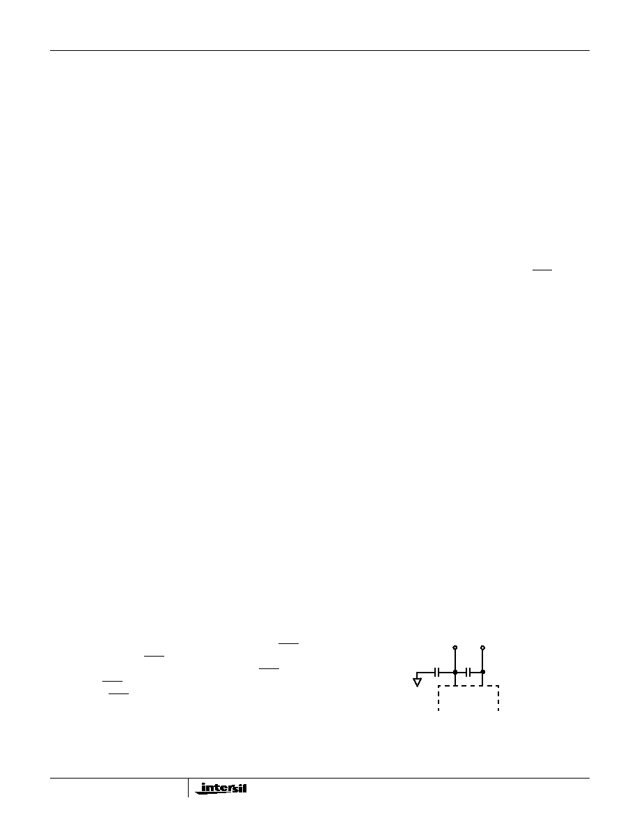
High Voltage Decoupling
The 100V rating of the device will require a capacitor of
higher voltage rating for decoupling. Suggested decoupling
values for all device pins are 0.1
µ
F. Standard surface mount
ceramic capacitors are rated at 100V. For applications driven
at low cost and small size, the decoupling scheme shown
below could be implemented.
As with all decoupling schemes, the capacitors should be as
close to the device pins as physically possible.
P
TO
V
BH
I
BHQ
◊
V
BL
I
BLQ
◊
V
CC
I
CCQ
◊
+
+
=
(EQ. 37)
FIGURE 11. ALTERNATE DECOUPLING SCHEME
VBH
VBL
0.22
µ
0.22
µ
HC5518X
HC55180, HC55181, HC55182, HC55183, HC55184
42
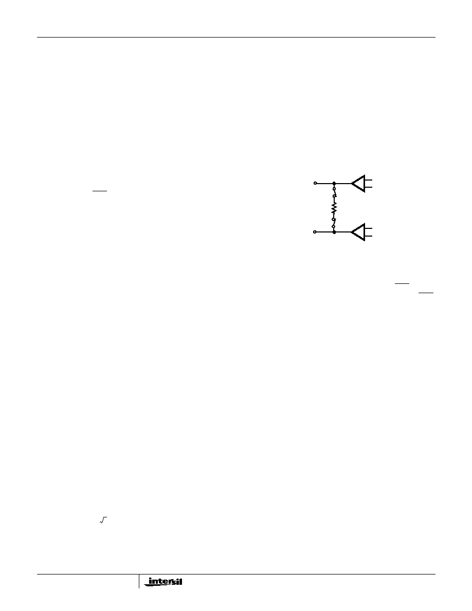
Uncommitted Switch
Overview
The uncommitted switch is a three terminal device designed
for flexibility. The independent logic control input, SWC,
allows switch operation regardless of device operating
mode. The switch is activated by a logic low. The positive
and negative terminals of the device are labeled SW+ and
SW- respectively.
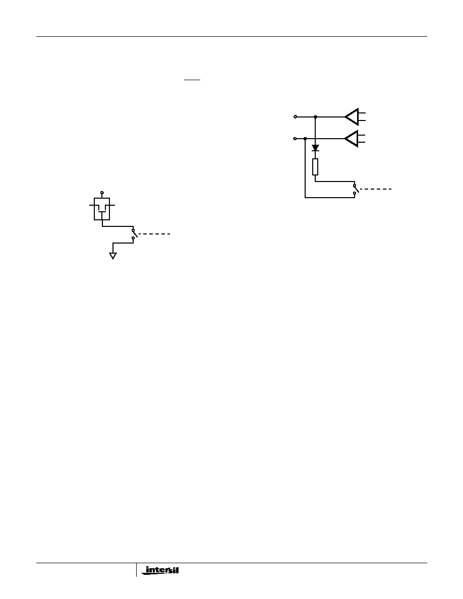
Relay Driver
The uncommitted switch may be used as a relay driver by
connecting SW+ to the relay coil and SW- to ground. The
switch is designed to have a maximum on voltage of 0.6V
with a load current of 45mA.
Since the device provides the ringing waveform, the relay
functions which may be supported include subscriber
disconnect, test access or line interface bypass. An external
snubber diode is not required when using the uncommitted
switch as a relay driver.
Test Load
The switch may be used to connect test loads across Tip
and Ring. The test loads can provide external test
termination for the device. Proper connection of the
uncommitted switch to Tip and Ring is shown below.
The diode in series with the test load blocks current from
flowing through the uncommitted switch when the polarity of
the Tip and Ring terminals are reversed. In addition to the
reverse active state, the polarity of Tip and Ring are reversed
for half of the ringing cycle. With independent logic control
and the blocking diode, the uncommitted switch may be
continuously connected to the Tip and Ring terminals.
FIGURE 12. EXTERNAL RELAY SWITCHING
RELAY
SW+
SW-
SWC
+5V
FIGURE 13. TEST LOAD SWITCHING
RING
TIP
TEST
LOAD
SW+
SW-
SWC
HC55180, HC55181, HC55182, HC55183, HC55184
43
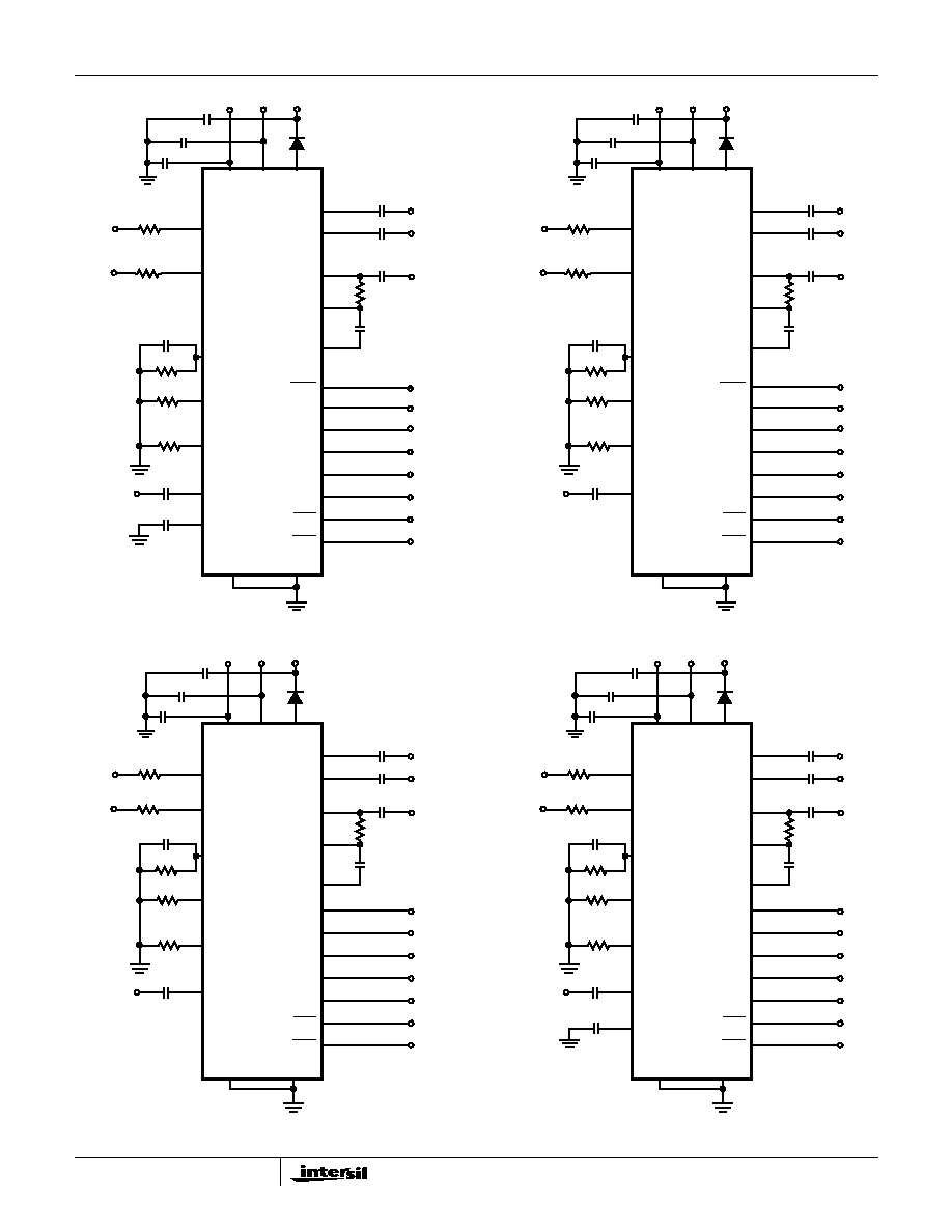
Basic Application Circuits
VRX
VRS
TIP
VFB
BGND
AGND
VCC
RING
VTX
-IN
VBL
VBH
RD
RTD
CDC
ILIM
E0
F2
F1
F0
FIGURE 14. HC55180 BASIC APPLICATION CIRCUIT
DET
ALM
HC55180
V
CC
POL
C
RX
C
RS
C
TX
R
IL
C
FB
R
S
R
SH
C
RT
R
RT
C
POL
C
PS1
C
DC
C
PS3
U
1
R
P1
R
P2
TABLE 2. BASIC APPLICATION CIRCUIT COMPONENT LIST
COMPONENT
VALUE
TOLERANCE
RATING
U1 - Ringing SLIC
HC5518x
N/A
N/A
R
RT
20k
1%
0.1W
R
SH
49.9k
1%
0.1W
R
IL
71.5k
1%
0.1W
R
S
210k
1%
0.1W
C
RX
, C
RS
, C
TX
, C
RT
, C
POL
, C
FB
0.47
µ
F
20%
10V
C
DC
4.7
µ
F
20%
10V
C
PS1
0.1
µ
F
20%
>100V
C
PS2
, C
PS3
0.1
µ
F
20%
100V
D
1
1N400X type with breakdown > 100V.
R
P1
, R
P2
Protection resistor values are application dependent and will be determined by protection re-
quirements. Standard applications will use
35
per side.
Design Parameters: Ring Trip Threshold = 90mA
PEAK
, Switch Hook Threshold = 12mA, Loop Current Limit = 24.6mA, Synthesize Device Im-
pedance = 210k
/400 = 525
, with 39
protection resistors, impedance across Tip and Ring terminals = 603
. Where applicable, these compo-
nent values apply to the Basic Application Circuits for the HC55180, HC55181, HC55182, HC55183 and HC55184. Pins not shown in the Basic
Application Circuit are no connect (NC) pins.
HC55180, HC55181, HC55182, HC55183, HC55184
44
VRX
VRS
TIP
VFB
BGND
AGND
RING
VTX
-IN
SW+
SW-
BSEL
RD
RTD
CDC
ILIM
E0
F2
F1
F0
FIGURE 15. HC55181 BASIC APPLICATION CIRCUIT
DET
ALM
HC55181
V
CC
POL
SWC
C
RX
C
RS
C
TX
R
IL
C
FB
R
S
R
SH
C
RT
R
RT
C
POL
C
DC
U
1
R
P1
R
P2
VCC
VBL
VBH
D
1
C
PS1
C
PS3
C
PS2
VRX
VRS
TIP
VFB
BGND
AGND
RING
VTX
-IN
BSEL
RD
RTD
CDC
ILIM
E0
F2
F1
F0
FIGURE 16. HC55183 BASIC APPLICATION CIRCUIT
DET
ALM
HC55183
V
CC
C
RX
C
RS
C
TX
R
IL
C
FB
R
S
R
SH
C
RT
R
RT
C
DC
U
1
R
P1
R
P2
VCC
VBL
VBH
D
1
C
PS1
C
PS3
C
PS2
VRX
VRS
TIP
VFB
BGND
AGND
RING
VTX
-IN
SW+
SW-
BSEL
RD
RTD
CDC
ILIM
E0
F2
F1
F0
FIGURE 17. HC55182 BASIC APPLICATION CIRCUIT
DET
ALM
HC55182
V
CC
SWC
C
RX
C
RS
C
TX
R
IL
C
FB
R
S
R
SH
C
RT
R
RT
C
DC
U
1
R
P1
R
P2
VCC
VBL
VBH
D
1
C
PS1
C
PS3
C
PS2
VRX
VRS
TIP
VFB
BGND
AGND
RING
VTX
-IN
BSEL
RD
RTD
CDC
ILIM
E0
F2
F1
F0
FIGURE 18. HC55184 BASIC APPLICATION CIRCUIT
DET
ALM
HC55184
V
CC
C
RX
C
RS
C
TX
R
IL
C
FB
R
S
R
SH
C
RT
R
RT
C
DC
U
1
R
P1
R
P2
VCC
VBL
VBH
D
1
C
PS1
C
PS3
C
PS2
POL
C
POL
HC55180, HC55181, HC55182, HC55183, HC55184

45
Additional Application Diagrams
Reducing Overhead Voltages
The transmission overhead voltage of the device is internally
set to 4V per side. The overhead voltage may be reduced by
injecting a negative DC voltage on the receive input using a
voltage divider (Fig. 19). Accordingly, the 2-wire port overload
level will decrease the same amount as the injected offset.
The divider shunt resistance is the parallel combination of
the internal 160k
resistor and the external R
2
. The sum of
R
1
and R
2
should be greater than 500k
to minimize the
additional power dissipation of the divider. The DC gain
relationship from the divider voltage, V
D
, to the Tip and Ring
outputs is shown below.
With a low battery voltage -24V and a divider voltage of
-0.5V, the Tip to Ring voltage is 17V. As a result, the
overhead voltage is reduced from 8V to 7V and the overload
level will decrease from 3.5V
PEAK
to 3.0V
PEAK
.
CODEC Ringing Generation
Maximum ringing amplitudes of the device are achieved with
signal levels approximately 2.4V
P-P
. Therefore the low pass
receive output of the CODEC may serve as the low level ring
generator. The ringing input impedance of 480k
minimum
should not interfere with CODEC drive capability. A single
external capacitor is required to AC coupled the ringing
signal from the CODEC. The circuit diagram for CODEC
ringing is shown below.
Implementing Teletax Signalling
A resistor, R
T
, is required at the -IN input of the device for
injecting the teletax signal (Figure 20). For most
applications the synthesized device impedance (i.e., 600
)
will not match the 200
teletax impedance. The gain set by
R
T
cancels the impedance matching feedback with respect
to the teletax injection point. Therefore the device appears
as a low impedance source for teletax. The resistor R
T
is
calculated using the following equation.
The signal level across a 200
load will be twice the injected
teletax signal level. As the teletax level at VTX will equal the
injection level, set R
C
= R
B
for cancellation. The value of R
B
is based on the voice band transhybrid balance
requirements. The connection of the teletax source to the
transhybrid amplifier should be AC coupled to allow proper
biasing of the transhybrid amplifier input
Ringing With DC Offsets
The balanced ringing waveform consists of zero DC offset
between the Tip and Ring terminals. However, the linear
amplifier architecture provides control of the DC offset
during ringing. The DC gain is the same as the AC gain,
40V/V per amplifier. Positive DC offsets applied directly to
the ringing input will shift both Tip and Ring away from half
battery towards ground and battery respectively. A voltage
divider on the ringing input may be used to generate the
offset (Figure 22). The reference voltage, V
REF
, can be
either the CODEC 2.4V reference voltage or the 5V supply.
An offset during ringing of 30V, would require a DC shift of
15V at Tip and 15V at Ring. The DC offset would be created
by a +0.375V (V
D
) at the VRS input. The divider resistors
should be selected to minimize the value of the AC coupling
capacitor C
RS
and the loading of the ring generator and
voltage reference. The ringing input impedance should also
be accounted for in divider resistor calculations.
FIGURE 19. EXTERNAL OVERHEAD CONTROL
HC5518X
VBL
FROM
CODEC
R
2
R
1
C
RX
V
D
160 k
1:1
VRX
V
T
R
≠
V
BL
8
2
V
D
◊
(
)
≠
≠
=
(EQ. 38)
FIGURE 20. CODEC RINGING INTERFACE
HC5518X
RX OUT
CODEC
160 k
1:1
VRS
+
-
480K
VRX
R
T
200
200
2
R
P
◊
R
S
400
/
(
)
+
+
-------------------------------------------------------------------
R
S
◊
=
(EQ. 39)
FIGURE 21. TELETAX SIGNALLING
+
-
R
F
R
B
CODEC
+2.4V
TX IN
-IN
VFB
VTX
+
-
RS
CFB
TA
RT
R
C
TELETAX
SOURCE
FIGURE 22. EXTERNAL OVERHEAD CONTROL
V
REF
FROM
RING GEN.
R
2
R
1
C
RS
V
D
HC5518X
VRS
+
-
480K
HC55180, HC55181, HC55182, HC55183, HC55184

46
All Intersil semiconductor products are manufactured, assembled and tested under ISO9000 quality systems certification.
Intersil semiconductor products are sold by description only. Intersil Corporation reserves the right to make changes in circuit design and/or specifications at any time with-
out notice. Accordingly, the reader is cautioned to verify that data sheets are current before placing orders. Information furnished by Intersil is believed to be accurate and
reliable. However, no responsibility is assumed by Intersil or its subsidiaries for its use; nor for any infringements of patents or other rights of third parties which may result
from its use. No license is granted by implication or otherwise under any patent or patent rights of Intersil or its subsidiaries.
For information regarding Intersil Corporation and its products, see web site http://www.intersil.com
Pin Descriptions
PLCC
SYMBOL
DESCRIPTION
1
TIP
TIP power amplifier output.
2
BGND
Battery Ground - To be connected to zero potential. All loop current and longitudinal current flow from this ground. Inter-
nally separate from AGND but it is recommended that it is connected to the same potential as AGND.
3
VBL
Low battery supply connection.
4
VBH
High battery supply connection for the most negative battery.
5
SW+
Uncommitted switch positive terminal. This pin is a no connect (NC) on the HC55180, HC55183 and HC55184.
6
SW-
Uncommitted switch negative terminal. This pin is a no connect (NC) on the HC55180, HC55183 and HC55184.
7
SWC
Switch control input. This TTL compatible input controls the uncommitted switch, with a logic "0" enabling the switch and
logic "1" disabling the switch. This pin is a no connect (NC) on the HC55180, HC55183 and HC55184.
8
F2
Mode control input - MSB. F2-F0 for the TTL compatible parallel control interface for controlling the various modes of
operation of the device.
9
F1
Mode control input.
10
F0
Mode control input.
11
E0
Detector Output Selection Input. This TTL input controls the multiplexing of the SHD (E0 = 1) and GKD (E0 = 0)
comparator outputs to the DET output based upon the state at the F2-F0 pins (see the Device Operating Modes table
shown on page 2).
12
DET
Detector Output - This TTL output provides on-hook/off-hook status of the loop based upon the selected operating mode.
The detected output will either be switch hook, ground key or ring trip (see the Device Operating Modes table shown on
page 2).
13
ALM
Thermal Shutdown Alarm. This pin signals the internal die temperature has exceeded safe operating temperature
(approximately 175
o
C) and the device has been powered down automatically.
14
AGND
Analog ground reference. This pin should be externally connected to BGND.
15
BSEL
Selects between high and low battery, with a logic "1" selecting the high battery and logic "0" the low battery. This pin is
a no connect (NC) on the HC55180.
16
NC
This pin is a no connect (NC) for all the devices.
17
POL
External capacitor on this pin sets the polarity reversal time. This pin is a no connect on the HC55182 and HC55183.
18
VRS
Ringing Signal Input - Analog input for driving 2-wire interface while in Ring Mode.
19
VRX
Analog Receive Voltage - 4-wire analog audio input voltage. AC couples to CODEC.
20
VTX
Transmit output voltage - Output of impedance matching amplifier, AC couples to CODEC.
21
VFB
Feedback voltage for impedance matching. This voltage is scaled to accomplish impedance matching.
22
-IN
Impedance matching amplifier summing node.
23
VCC
Positive voltage power supply, usually +5V.
24
CDC
DC Biasing Filter Capacitor - Connects between this pin and V
CC
.
25
RTD
Ring trip filter network.
26
ILIM
Loop Current Limit programming resistor.
27
RD
Switch hook detection threshold programming resistor.
28
RING
RING power amplifier output.
HC55180, HC55181, HC55182, HC55183, HC55184