
1
Æ
HC-55564/883
Continuously Variable Slope
Delta-Modulator (CVSD)
The HC-55564/883 is a half duplex modulator/demodulator
CMOS intergrated circuit used to convert voice signals into
serial NRZ digital data and to reconvert that data into voice.
The conversion is by delta-modulation, using the
Continuously Variable Slope (CVSD) method of
modulation/demodulation.
While the signals are compatible with other CVSD circuits,
the internal design is unique. The analog loop filters have
been replaced by very low power digital filters which require
no external timing components. This approach allows
inclusion of many desirable features which would be difficult
to implement using other approaches.
The fundamental advantages of delta-modulation, along with
its simplicity and serial data format, provide an efficient (low
data rate/low memory requirements) method for voice
digitization. The device may be easily configured with the
National TP3040 PCM/CVSD filter.
The HC-55564/883 is usable from 9k bits/sec to above
64kbps. For more applications information, see Application
Notes AN576 and AN607.
Features
∑ This Circuit is Processed in Accordance to MIL-STD-883
and is Fully Conformant Under the Provisions of Para-
graph 1.2.1.Requires Few External Parts
∑ All Digital
∑ Requires Few External Parts
∑ Low Power Drain
∑ Time Constants Determined by Clock Frequency; No Cali-
bration or Drift Problems: Automatic Offset Adjustment
∑ Half Duplex Operation Under Digital Control
∑ Filter Reset Under Digital Control
∑ Automatic Overload Recovery
∑ Automatic "Quiet" Pattern Generation
∑ AGC Control Signal Available
Applications
∑ Voice Transmission Over Data Channels (Modems)
∑ Voice/Data Multiplexing (Pair Gain)
∑ Voice Encryption/Scrambling
∑ Voicemail
∑ Audio Manipulations: Delay Lines, Time Compression,
Echo Generation/Suppression, Special Effects, etc.
∑ Pagers/Satellites
∑ Data Acquisition Systems
∑ Voice I/O for Digital Systems and Speech Synthesis
Requiring Small Size, Low Weight, and Ease of Repro-
grammability
Pinouts
Ordering Information
PART
NUMBER
TEMPERATURE
RANGE
PACKAGE
HC1-55564/883
-55
o
C to +125
o
C
14 Lead CerDIP
HC4-55564/883
-55
o
C to +125
o
C
20 Lead Ceramic LCC
HC-55564/883
(CERDIP)
TOP VIEW
HC-55564/883
(CLCC)
TOP VIEW
V
DD
ANALOG GND
A
OUT
AGC
A
IN
NC
NC
DIG OUT
FZ
DIG IN
APT
ENC/DEC
CLOCK
DIG GND
1
2
3
4
5
6
7
14
13
12
11
10
9
8
3
4
5
6
7
9 10 11 12
2
20
1
19
8
15
14
18
17
16
13
NC
V
DD
ANALOG GND
DIG
I
T
A
L
FZ
A
OUT
NC
AGC
NC
A
IN
DIGITAL IN
NC
APT
NC
ENCODE/DECODE
CLOCK
NC
DI
G
I
T
A
L
NC
NC
OU
T
GN
D
October 1999
FN3738.1
OBSO
LETE
PRO
DUCT
NO R
ECOM
MEND
ED RE
PLAC
EMEN
T
conta
ct our
Tech
nical
Supp
ort Ce
nter a
t
CAUTION: These devices are sensitive to electrostatic discharge; follow proper IC Handling Procedures.
1-888-INTERSIL or 321-724-7143
|
Intersil (and design) is a trademark of Intersil Americas Inc.
Copyright © Intersil Americas Inc. 2002. All Rights Reserved
1-888
-INTE
RSIL
or ww
w.inte
rsil.co
m/tsc
2
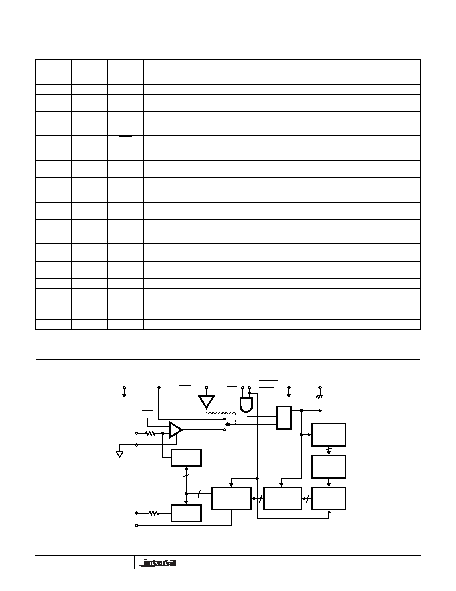
Functional Diagram
Pin Description
PIN NO.
14 LEAD
DIP
PIN NO.
20 LEAD
LCC
SYMBOL
DESCRIPTION
1
2
V
DD
Positive Supply Voltage. Voltage range is +3.2V to +6.0V.
2
3
Analog
GND
Analog Ground connection to D/A ladders and comparator.
3
4
A
OUT
Audio Out recovered from 10-bit DAC. May be used as side tone at the transmitter. Presents
approximately 75k
source with DC offset of V
DD
/2. Within
±
2dB of Audio Input. Should be externally
AC coupled.
4
6
AGC
Automatic Gain Control output. A logic low level will appear at this output when the recovered signal ex-
cursion reaches one-half of full scale value. In each half cycle full scale is V
DD
/2. The mark-space ratio
is proportional to the average signal level.
5
8
A
IN
Audio Input to comparator. Should be externally AC coupled. Presents approximately 200k
in series
with V
DD
/2.
6, 7
1, 5, 7, 9,
10, 11, 15,
17
NC
No internal connection is made to these pins.
8
12
Digital
GND
Logic ground. 0V reference for all logic inputs and outputs.
9
13
Clock
Sampling rate clock. In the decode mode, must be synchronized with the digital input data such that the
data is valid at the positive clock transition. In the encode mode, the digital data is clocked out on the
negative going clock transition. The clock rate equals the data rate.
10
14
Encode/
Decode
A single CVSD can provide half-duplex operation. The encode or decode function is selected by the logic
level applied to this input. A low level selects the encode mode, a high level the decode mode.
11
16
APT
Alternate Plain Text input. Activating this input caused a digital quieting pattern to be transmitted, however;
internally the CVSD is still functional and a signal is still available at the A
OUT
port. Active low.
12
18
Digital In
Input for the received digital NRZ data.
13
19
FZ
Force Zero input. Activating this input resets the internal logic and forces the digital output and the recov-
ered audio output into the "quieting" condition. An alternating 1-0 pattern appears at the digital output at
1/2 the clock rate. When this is decoded by a receive CVSD, a 10mV
P-P
inaudible signal appears at audio
output. Active low.
14
20
Digital Out
Output for transmitted digital NRZ data.
NOTE:
1. No active input should be left in a "floating condition".
3-BIT
SHIFT
STEP
SIZE
SYLLABIC
FILTER
4ms
REGISTER
LOGIC
DIGITAL
MODULATOR
±
1
SIGNAL
ESTIMATE
FILTER 1ms
10-BIT
DAC
APT
(14)
DIGITAL
OUT
F/F
RESET
6
Z
OUT
10
D
T
RESET
10-BIT
DAC
10
(3) A
OUT
(SIDE TONE)
(4) AGC OUT
Q
FORCE
ZERO
(9)
DIGITAL
GND
(10)
ENC/DEC
(11) (13)
CLOCK
(8)
(12)
DIGITAL
(1)
V
DD
3V TO 6V
Z
IN
ANALOG
GND
(2)
(5)
A
IN
V
DD
2
COMPARATOR
IN
RESET
HC-55564/883
3
Absolute Maximum Ratings
Thermal Information
Voltage at Any Pin . . . . . . . . . . . . . . . . . . .GND -0.3V to V
DD
+0.3V
Maximum V
DD
Voltage . . . . . . . . . . . . . . . . . . . . . . . . . . . . . . +6.0V
Minimum V
DD
Voltage . . . . . . . . . . . . . . . . . . . . . . . . . . . . . . . +3.2V
Junction Temperature . . . . . . . . . . . . . . . . . . . . . . . . . . . . . .+175
o
C
Storage Temperature Range . . . . . . . . . . . . . . . . . -65
o
C to +150
o
C
Lead Temperature (Soldering 10s) . . . . . . . . . . . . . . . . . . . .+300
o
C
ESD Rating . . . . . . . . . . . . . . . . . . . . . . . . . . . . . . . . . . . . . .<2000V
Thermal Resistance
JA
JC
CerDIP Package . . . . . . . . . . . . . . . . . . .
66
o
C/W
16
o
C/W
Ceramic LCC Package . . . . . . . . . . . . . .
65
o
C/W
15
o
C/W
Package Power Dissipation Limit at +75
o
C for T
J
at
+175
o
C
CerDIP Package . . . . . . . . . . . . . . . . . . . . . . . . . . . . . . . . . 1.52W
Ceramic LCC Package . . . . . . . . . . . . . . . . . . . . . . . . . . . . 1.54W
Package Power Dissipation Derating Factor Above +75
o
C
CerDIP Package . . . . . . . . . . . . . . . . . . . . . . . . . . . . . . 15.2W/
o
C
Ceramic LCC Package . . . . . . . . . . . . . . . . . . . . . . . . . 15.4W/
o
C
CAUTION: Stresses above those listed in "Absolute Maximum Ratings" may cause permanent damage to the device. This is a stress only rating and operation of the
device at these or any other conditions above those indicated in the operational sections of this specification is not implied.
Recommended Operating Conditions
Operating Temperature Range . . . . . . . . . . . . . . . -55
o
C to +125
o
C
Operating Supply Voltage (V
DD
Range)
. . . . . . . . . . . +
3.2V to
+
6.0V
TABLE 1. DC ELECTRICAL PERFORMANCE CHARACTERISTICS
Device Tested at: V
SUPPLY
= +5V, fclk = 16kHz, Operating Temperature = -55
o
C
T
A
+125
o
C, Unless Otherwise Specified.
PARAMETER
SYMBOL
CONDITIONS
GROUP A
SUBGROUP
TEMPERATURE
LIMITS
UNITS
TYP
MAX
Supply Current
I
DD
Encode Mode: A
IN
= 0V
1
+25
o
C
-
1.5
mA
2, 3
+125
o
C, -55
o
C
-
1.5
mA
Logic Input High (Note 2)
V
IH
Input Level: `1' = +3.5V,
`0' = +1.5V
1
+25
o
C
3.5
-
V
2, 3
+125
o
C, -55
o
C
3.5
-
V
Logic Input Low (Note 2)
V
IL
Input Level: `1' = +3.5V,
`0' = +1.5V
1
+25
o
C
-
1.5
V
2, 3
+125
o
C, -55
o
C
-
1.5
V
Logic Output High (Note 3)
V
OH
I
LOAD
= -40
µ
A
1
+25
o
C
4.0
-
V
2, 3
+125
o
C, -55
o
C
4.0
-
V
Logic Output Low (Note 3)
V
OL
I
LOAD
= +0.8mA
1
+25
o
C
-
0.4
V
2, 3
+125
o
C, -55
o
C
-
0.4
V
Quieting Pattern
Amplitude (Note 8)
V
QP
FZ = 0; Clock Inputs
Switched Statically
1
+25
o
C
-
14
mV
P-P
2, 3
+125
o
C, -55
o
C
-
14
mV
P-P
AGC Threshold (Note 9)
V
ATH
Encode Mode
1
+25
o
C
0.45
0.65
F.S.
2, 3
+125
o
C, -55
o
C
0.45
0.65
F.S.
TABLE 2. AC ELECTRICAL PERFORMANCE CHARACTERISTICS
Table 2 Intentionally Left Blank.
TABLE 3. ELECTRICL PERFORMANCE CHARACTERISTICS
Devices Characterized at: V
DD
= +5.0V, T
A
= +25
o
C, Operating Temperature, fclk = 16kHz Clock Sampling Rate.
ENC/DDC = ENC = Encode Mode, Unless Otherwise Specified.
PARAMETER
SYMBOL
CONDITIONS
NOTE
TEMPERATURE
LIMITS
UNITS
TYP
MAX
Sampling Rate
CLK
A
IN
= 0.775 V
RMS
at 20Hz
1, 12
+25
o
C
9
64
kBS
+125
o
C, -55
o
C
9
64
kBS
CLK Duty Cycle
A
IN
= 0.775 V
RMS
at
100Hz
12
+25
o
C
30
70
%
+125
o
C, -55
o
C
30
70
%
HC-55564/883

4
Audio Input Voltage
A
IN
A
IN
= 100Hz
4, 12
+25
o
C
-
1.2
V
RMS
+125
o
C, -55
o
C
-
1.2
V
RMS
Audio Output Voltage
A
OUT
A
IN
= 100Hz
5, 12
+25
o
C
-
1.2
V
RMS
+125
o
C, -55
o
C
-
1.2
V
RMS
Input Impedance
Z
IN
A
IN
= 100Hz
6, 12
+25
o
C
150
500
k
+125
o
C, -55
o
C
150
500
k
Output Impedance
Z
OUT
A
IN
= 100Hz
6, 12
+25
o
C
35
25
k
+125
o
C, -55
o
C
35
25
k
Transfer Gain
A
E-D
A
IN
= 0.775 V
RMS
at
100Hz
11, 12
+25
o
C
-2
+2
dB
-55
o
C, +125
o
C
-2
+2
dB
Resolution
RES
A
IN
at 100Hz. Note 8
12, 13
+25
o
C
0.3
-
% of
Supply
MIN Step Size
MSS
7, 12
+25
o
C
0.10
0.14
% of
Supply
Clamping Threshold
V
CTH
10, 12
+25
o
C
0.70
0.90
F.S.
NOTES:
1. There is one NRZ (Non-Return Zero) data bit per clock period. Data is clocked out on the negative clock edge. Data is clocked into the CVSD
on the positive going edge (see Figure 2). Clock may be run at less than 9kbps.
2. Logic inputs are CMOS compatible at supply voltage and are diode protected. Digital data input is NRZ at clock rate.
3. Logic outputs are CMOS compatible at supply voltage and will withstand short-circuits to V
DD
or ground; however, the short circuit duty cycle
must not exceed 5% in order to maintain an acceptable current density level. Digital data output is NRZ and changes with negative clock tran-
sitions. Each output will drive one LS TTL loads.
4. Recommended voice input range for best voice performance. Should be externally AC coupled.
5. May be used for side-tone in encode mode. Should be externally AC coupled.
6. Presents series impedance with audio signal. Zero signal reference is approximately V
DD
/2. Varies with audio input level by
±
2dB.
7. The minimum audio output voltage change that can be produced by the internal DAC.
8. The "quieting" pattern or idle-channel audio output steps at 1/2 the bit rate, changing state on negative clock transitions.
9. A logic "0" will appear at the AGC output pin when the recovered signal reaches one-half of full-scale value (positive or negative), i.e. at V
DD
/2
±
25% of V
DD
.
10. The recovered signal will be clamped, and the computation will be inhibited, when the recovered signal reaches three-quarters of full-scale val-
ue, and will unclamp when it falls below this value (positive or negative).
11. No load condition measured from audio in to audio out.
12. The parameters listed in this table are controlled via design or process parameters and are not directly tested. These parameters are charac-
terized upon initial design release and upon design changes which would affect these characteristics.
13. The minimum audio input voltage above which encoding is guaranteed to take place.
TABLE 4. ELECTRICAL TEST REQUIREMENTS
MIL-STD-883 TEST REQUIREMENTS
SUBGROUPS (SEE TABLE 1)
Interim Electrical Parameters (Pre Burn-In)
1
Final Electrical Test Parameters
1 (Note 1), 2, 3
Group A Test Requirements
1, 2, 3
Groups C and D Endpoints
1
NOTE:
1. PDA applies to Subgroup 1 only.
TABLE 3. ELECTRICL PERFORMANCE CHARACTERISTICS (Continued)
Devices Characterized at: V
DD
= +5.0V, T
A
= +25
o
C, Operating Temperature, fclk = 16kHz Clock Sampling Rate.
ENC/DDC = ENC = Encode Mode, Unless Otherwise Specified. (Continued)
PARAMETER
SYMBOL
CONDITIONS
NOTE
TEMPERATURE
LIMITS
UNITS
TYP
MAX
HC-55564/883

5
Die Characteristics
DIE DIMENSIONS:
82 x 147 x 20 ± 1 mils
METALLIZATION:
Type: AlSi
Thickness: 10k≈ ± 1k≈
GLASSIVATION:
Type: Silane, 3% Phosphorous
Thickness: 13k≈ ± 2.6k≈
WORST CASE CURRENT DENSITY:
2.0 x 10⁵A/cm2
TRANSISTOR COUNT: 1896
PROCESS: CMOS; SAJI
Metallization Mask Layout
HC-55564/883
A
OUT
ANALOG
V
DD
DIGITAL
FZ
DIGITAL IN
APT
ENC/DEC
CLOCK
A
IN
AGC
OUT
GND
DIGITAL
GND
HC-55564/883