 | –≠–ª–µ–∫—Ç—Ä–æ–Ω–Ω—ã–π –∫–æ–º–ø–æ–Ω–µ–Ω—Ç: HCS05MS | –°–∫–∞—á–∞—Ç—å:  PDF PDF  ZIP ZIP |

35
CAUTION: These devices are sensitive to electrostatic discharge; follow proper IC Handling Procedures.
1-888-INTERSIL or 321-724-7143 | Copyright © Intersil Corporation 1999
HCS05MS
Radiation Hardened
Hex Inverter with Open Drain
Pinouts
14 LEAD CERAMIC DUAL-IN-LINE
METAL SEAL PACKAGE (SBDIP)
MIL-STD-1835 CDIP2-T14, LEAD FINISH C
TOP VIEW
14 LEAD CERAMIC METAL SEAL
FLATPACK PACKAGE (FLATPACK)
MIL-STD-1835 CDFP3-F14, LEAD FINISH C
TOP VIEW
Functional Diagram
TRUTH TABLE
INPUTS
OUTPUTS
An
Yn
L
Z (Note 1)
H (Note 2)
H
L
NOTES:
1. No pullup resistor
2. With pullup resistor
3. L = Low
4. H = High
A1
Y1
A2
Y2
A3
Y3
GND
VCC
A6
Y6
A5
Y5
A4
Y4
1
2
3
4
5
6
7
14
13
12
11
10
9
8
14
13
12
11
10
9
8
2
3
4
5
6
7
1
A1
Y1
A2
Y2
A3
Y3
GND
VCC
A6
Y6
A5
Y5
A4
Y4
An
Yn
Features
∑ 3 Micron Radiation Hardened SOS CMOS
∑ Total Dose 200K RAD (Si)
∑ SEP Effective LET No Upsets: >100 MEV-cm
2
/mg
∑ Single Event Upset (SEU) Immunity < 2 x 10
-9
Errors/Bit-Day
(Typ)
∑ Dose Rate Survivability: >1 x 10
12
RAD (Si)/s
∑ Dose Rate Upset >10
10
RAD (Si)/s 20ns Pulse
∑ Latch-Up Free Under Any Conditions
∑ Military Temperature Range: -55
o
C to +125
o
C
∑ Significant Power Reduction Compared to LSTTL ICs
∑ DC Operating Voltage Range: 4.5V to 5.5V
∑ Input Logic Levels
- VIL = 30% of VCC Max
- VIH = 70% of VCC Min
∑ Input Current Levels Ii
5
µ
A at VOL, VOH
Description
The Intersil HCS05MS is a Radiation Hardened Hex inverter
function with open drain outputs. These open drain outputs can
drive into resistive loads with a separate voltage supply.
The HCS05MS utilizes advanced CMOS/SOS technology to
achieve high-speed operation. This device is a member of
radiation hardened, high-speed, CMOS/SOS Logic Family.
The HCS05MS is supplied in a 14 lead Ceramic Flatpack (K suffix)
or a Ceramic Dual-In-Line Package (D suffix).
Ordering Information
PART
NUMBER
TEMPERATURE
RANGE
SCREENING
LEVEL
PACKAGE
HCS05DMSR
-55
o
C to +125
o
C
Intersil Class
S Equivalent
14 Lead SBDIP
HCS05KMSR
-55
o
C to +125
o
C
Intersil Class
S Equivalent
14 Lead Ceramic
Flatpack
HCS05D/
Sample
+25
o
C
Sample
14 Lead SBDIP
HCS05K/
Sample
+25
o
C
Sample
14 Lead Ceramic
Flatpack
HCS05HMSR
+25
o
C
Die
Die
September 1995
Spec Number
518829
File Number
3557.1
36
Specifications HCS05MS
Absolute Maximum Ratings
Reliability Information
Supply Voltage . . . . . . . . . . . . . . . . . . . . . . . . . . . . . . -0.5V to +7.0V
Input Voltage Range, All Inputs . . . . . . . . . . . . .-0.5V to VCC +0.5V
DC Input Current, Any One Input
. . . . . . . . . . . . . . . . . . . . . . . .±
10mA
DC Drain Current, Any One Output
. . . . . . . . . . . . . . . . . . . . . . .±
25mA
(All Voltage Reference to the VSS Terminal)
Storage Temperature Range (TSTG) . . . . . . . . . . . -65
o
C to +150
o
C
Junction Temperature (TJ) . . . . . . . . . . . . . . . . . . . . . . . . . . +175
o
C
Lead Temperature (Soldering 10sec) . . . . . . . . . . . . . . . . . . +265
o
C
ESD Classification . . . . . . . . . . . . . . . . . . . . . . . . . . . . . . . . Class 1
Thermal Resistance
JA
JC
SBDIP Package. . . . . . . . . . . . . . . . . . . .
74
o
C/W
24
o
C/W
Ceramic Flatpack Package . . . . . . . . . . .
116
o
C/W
30
o
C/W
Maximum Package Power Dissipation at +125
o
C Ambient
SBDIP Package. . . . . . . . . . . . . . . . . . . . . . . . . . . . . . . . . . 0.68W
Ceramic Flatpack Package . . . . . . . . . . . . . . . . . . . . . . . . . 0.43W
If device power exceeds package dissipation capability, provide heat
sinking or derate linearly at the following rate:
SBDIP Package. . . . . . . . . . . . . . . . . . . . . . . . . . . . . . 13.5mW/
o
C
Ceramic Flatpack Package . . . . . . . . . . . . . . . . . . . . . . 8.6mW/
o
C
CAUTION: As with all semiconductors, stress listed under "Absolute Maximum Ratings" may be applied to devices (one at a time) without resulting in permanent
damage. This is a stress rating only. Exposure to absolute maximum rating conditions for extended periods may affect device reliability. The conditions listed
under "Electrical Performance Characteristics" are the only conditions recommended for satisfactory device operation..
Operating Conditions
Supply Voltage . . . . . . . . . . . . . . . . . . . . . . . . . . . . . +4.5V to +5.5V
Input Rise and Fall Times at 4.5V VCC (TR, TF) . . . . . 100ns/V Max
Operating Temperature Range (T
A
) . . . . . . . . . . . . -55
o
C to +125
o
C
Input High Voltage (VIH) . . . . . . . . . . . . . . . . . . . . . . . . 70% of VCC
Input Low Voltage (VIL). . . . . . . . . . . . . . . . . . . 0.0V to 30% of VCC
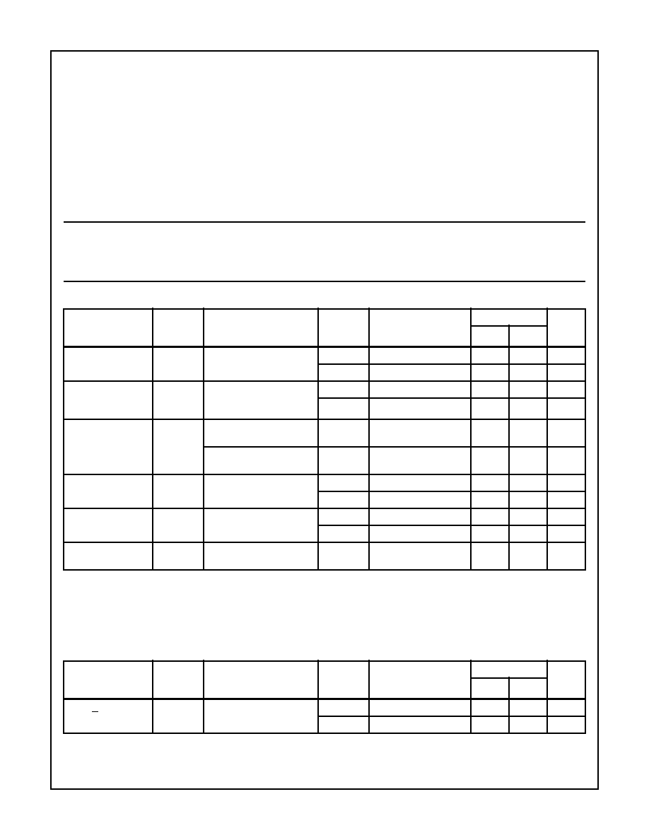
TABLE 1. DC ELECTRICAL PERFORMANCE CHARACTERISTICS
PARAMETER
SYMBOL
(NOTE 1)
CONDITIONS
GROUP
A SUB-
GROUPS
TEMPERATURE
LIMITS
UNITS
MIN
MAX
Supply Current
ICC
VCC = 5.5V,
VIN = VCC or GND
1
+25
o
C
-
10
µ
A
2, 3
+125
o
C, -55
o
C
-
200
µ
A
Output Current
(Sink)
IOL
VCC = VIH = 4.5V,
VOUT = 0.4V, VIL = 0V
(Note 2)
1
+25
o
C
4.8
-
mA
2, 3
+125
o
C, -55
o
C
4.0
-
mA
Output Voltage Low
VOL
VCC = 5.5V, VIH = 3.85V,
VIL = 1.35V, IOL = 50
µ
A
1, 2, 3
+25
o
C, +125
o
C, -55
o
C
-
0.1
V
VCC = 4.5V, VIH = 3.15V,
VIL = 1.35V, IOL = 50
µ
A,
1, 2, 3
+25
o
C, +125
o
C, -55
o
C
-
0.1
V
Input Leakage
Current
IIN
VCC = 5.5V, VIN = VCC or
GND
1
+25
o
C
-
±
0.5
µ
A
2, 3
+125
o
C, -55
o
C
-
±
5.0
µ
A
Three-State Output
Leakage Current
IOZH
VCC = 5.5V,
Force Voltage = VCC
1
+25
o
C
-
1
µ
A
2, 3
+125
o
C, -55
o
C
-
50
µ
A
Noise Immunity
Functional Test
FN
VCC = 4.5V, VIH = 3.15,
VIL = 1.35 (Note 3)
7, 8A, 8B
+25
o
C, +125
o
C, -55
o
C
-
-
V
NOTES:
1. All voltages reference to device GND.
2. Force/Measure functions may be interchanged.
3. For functional tests, VO
4.0V is recognized as a logic "1", and VO
0.5V is recognized as a logic "0".
TABLE 2. AC ELECTRICAL PERFORMANCE CHARACTERISTICS
PARAMETER
SYMBOL
(NOTES 1, 2)
CONDITIONS
GROUP
A SUB-
GROUPS
TEMPERATURE
LIMITS
UNITS
MIN
MAX
Propagation Delay
An to Yn
TPLZ
TPZL
VCC = 4.5V, VIH = 4.5V,
VIL = 0V
9
+25
o
C
2
18
ns
10, 11
+125
o
C, -55
o
C
2
20
ns
NOTES:
1. All voltages referenced to device GND.
2. Measurements assume RL = 500
, CL = 50pF, Input TR = TF = 3ns.
Spec Number
518829
37
Specifications HCS05MS
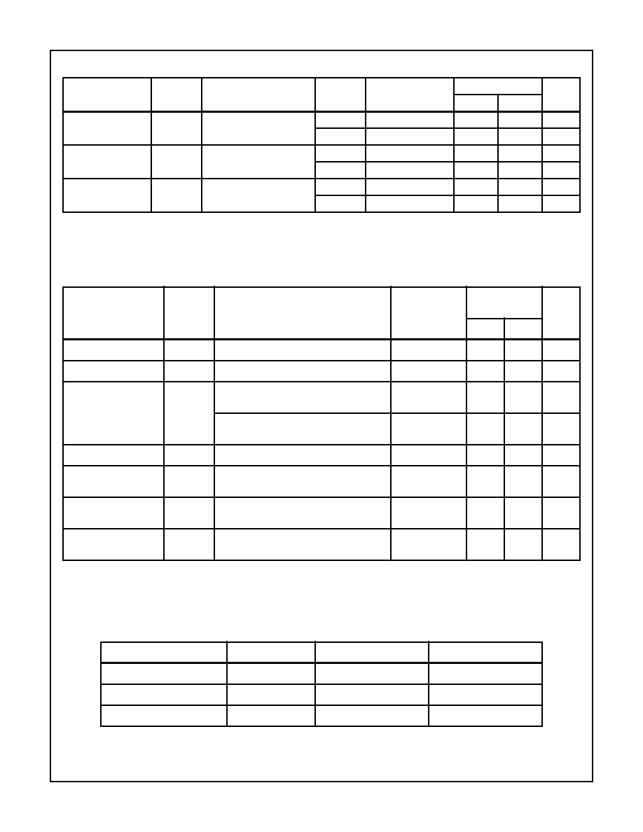
TABLE 3. ELECTRICAL PERFORMANCE CHARACTERISTICS
PARAMETER
SYMBOL
CONDITIONS
NOTES
TEMPERATURE
LIMITS
UNITS
MIN
MAX
Capacitance Power
Dissipation
CPD
VCC = 5.0V, VIH = 5.0V,
VIL = 0.0V, f = 1MHz
1
+25
o
C
-
15
pF
1
+125
o
C, -55
o
C
-
23
pF
Input Capacitance
CIN
VCC = 5.0V, VIH = 5.0V,
VIL = 0.0V, f = 1MHz
1
+25
o
C
-
10
pF
1
+125
o
C, -55
o
C
-
10
pF
Output Transition
Time
TTHL
VCC = 4.5V, VIH = 4.5V,
VIL = 0.0V
1
+25
o
C
1
15
ns
1
+125
o
C, -55
o
C
1
22
ns
NOTE:
1. The parameters listed in Table 3 are controlled via design or process parameters. Min and Max Limits are guaranteed but not directly
tested. These parameters are characterized upon initial design release and upon design changes which affect these characteristics.
TABLE 4. POST IRRADIATION ELECTRICAL PERFORMANCE CHARACTERISTICS
PARAMETER
SYMBOL
(NOTE 1)
CONDITIONS
TEMPERATURE
200K RAD
LIMITS
UNITS
MIN
MAX
Supply Current
ICC
VCC = 5.5V, VIN = VCC or GND
+25
o
C
-
0.2
mA
Output Current (Sink)
IOL
VCC = VIH = 4.5V, VOUT = 0.4V, VIL = 0V
+25
o
C
4.0
-
mA
Output Voltage Low
VOL
VCC = 5.5V , VIH = 3.85V, VIL = 1.65V,
IOL = 50
µ
A
+25
o
C
-
0.1
V
VCC = 4.5V , VIH = 3.15V, VIL = 1.35V,
IOL = 50
µ
A
+25
o
C
-
0.1
V
Input Leakage Current
IIN
VCC = 5.5V, VIN = VCC or GND
+25
o
C
-
±
5
µ
A
Three-State Output
Leakage Current
IOZH
VCC = 5.5V, Force Voltage = 0V or VCC
+25
o
C
-
±
50
µ
A
Noise Immunity
Functional Test
FN
VCC = 4.5V, VIH =3.15V, VIL = 1.35V,
(Note 2)
+25
o
C
-
-
V
Propagation Delay
TPLZ
TPZL
VCC = 4.5V, VIH =4.5V, VIL = 0V
+25
o
C
2
20
ns
NOTES:
1. All voltages referenced to device GND.
2. For functional tests, VO
4.0V is recognized as a logic "1", and VO
0.5V is recognized as a logic "0".
TABLE 5. DELTA PARAMETERS (+25
o
C)
PARAMETER
SYMBOL
GROUP B SUBGROUP
UNITS
Supply Current
ICC
+3
µ
A
Three-State Leaking Current
IOZH
±
200
nA
Output Current
IOL
-15
%
Spec Number
518829

38
Specifications HCS05MS
TABLE 6. APPLICABLE SUBGROUPS
CONFORMANCE GROUPS
METHOD
GROUP A SUBGROUPS
READ AND RECORD
Initial Test (Preburn-In)
100%/5004
1, 7, 9
ICC, IOL, IOZH
Interim Test
I
(Postburn-In)
100%/5004
1, 7, 9
ICC, IOL, IOZH
Interim Test
II
(Postburn-In)
100%/5004
1, 7, 9
ICC, IOL/H
PDA
100%/5004
1, 7, 9, Deltas
Interim Test
III
(Postburn-In)
100%/5004
1, 7, 9
ICC, IOL, IOZH
PDA
100%/5004
1, 7, 9, Deltas
Final Test
100%/5004
2, 3, 8A, 8B, 10, 11
Group A (Note 1)
Sample/5005
1, 2, 3, 7, 8A, 8B, 9, 10, 11
Group B
Subgroup B-5
Sample/5005
1, 2, 3, 7, 8A, 8B, 9, 10, 11, Deltas
Subgroups 1, 2, 3, 9, 10, 11
Subgroup B-6
Sample/5005
1, 7, 9
Group D
Sample/5005
1, 7, 9
NOTE:
1. Alternate Group A testing in accordance with Method 5005 of MIL-STD-883 may be exercised.
TABLE 7. TOTAL DOSE IRRADIATION
CONFORMANCE
GROUPS
METHOD
TEST
READ AND RECORD
PRE RAD
POST RAD
PRE RAD
POST RAD
Group E Subgroup 2
5005
1, 7, 9
Table 4
1, 9
Table 4 (Note 1)
NOTE:
1. Except FN test which will be performed 100% Go/No-Go.
TABLE 8. STATIC AND DYNAMIC BURN-IN TEST CONNECTIONS
OPEN
GROUND
VCC = 6V
±
0.5V
1/2 VCC = 3V
±
0.5V
OSCILLATOR
50kHz
25kHz
STATIC BURN-IN I TEST CONDITIONS (Note 1)
-
1, 3, 5, 7, 9, 11, 13
2, 4, 6, 8, 10, 12, 14
-
-
-
STATIC BURN-IN II TEST CONNECTIONS (Note 1)
2, 4, 6, 8, 10, 12
7
1, 3, 5, 9, 11, 13, 14
-
-
-
DYNAMIC BURN-IN I TEST CONNECTIONS (Note 2)
-
7
14
2, 4, 6, 8, 10, 12
1, 3, 5, 9, 11, 13
-
NOTES:
1. Each pin except VCC and GND will have a series resistor of 10K
±
5%.
2. Each pin except VCC and GND will have a series resistor of 1K
±
5%.
TABLE 9. IRRADIATION TEST CONNECTIONS
FUNCTION
OPEN
GROUND
VCC = 5V
±
0.5V
Irradiation Circuit
(Note 1)
2, 4, 6, 8, 10, 12
7
1, 3, 5, 9, 11, 13, 14
NOTE: Each pin except VCC and GND will have a resistor of 47K
±
5% for irradiation testing. Group E, Subgroup 2, sample
size is 4 dice/wafe,r 0 failures.
Spec Number
518829

39
HCS05MS
Intersil Space Level Product Flow - `MS'
Wafer Lot Acceptance (All Lots) Method 5007
(Includes SEM)
GAMMA Radiation Verification (Each Wafer) Method 1019,
4 Samples/Wafer, 0 Rejects
100% Nondestructive Bond Pull, Method 2023
Sample - Wire Bond Pull Monitor, Method 2011
Sample - Die Shear Monitor, Method 2019 or 2027
100% Internal Visual Inspection, Method 2010, Condition A
100% Temperature Cycle, Method 1010, Condition C,
10 Cycles
100% Constant Acceleration, Method 2001, Condition per
Method 5004
100% PIND, Method 2020, Condition A
100% External Visual
100% Serialization
100% Initial Electrical Test (T0)
100% Static Burn-In 1, Condition A or B, 24 hrs. min.,
+125
o
C min., Method 1015
100% Interim Electrical Test 1 (T1)
100% Delta Calculation (T0-T1)
100% Static Burn-In 2, Condition A or B, 24 hrs. min.,
+125
o
C min., Method 1015
100% Interim Electrical Test 2 (T2)
100% Delta Calculation (T0-T2)
100% PDA 1, Method 5004 (Notes 1and 2)
100% Dynamic Burn-In, Condition D, 240 hrs., +125
o
C or
Equivalent, Method 1015
100% Interim Electrical Test 3 (T3)
100% Delta Calculation (T0-T3)
100% PDA 2, Method 5004 (Note 2)
100% Final Electrical Test
100% Fine/Gross Leak, Method 1014
100% Radiographic, Method 2012 (Note 3)
100% External Visual, Method 2009
Sample - Group A, Method 5005 (Note 4)
100% Data Package Generation (Note 5)
NOTES:
1. Failures from Interim electrical test 1 and 2 are combined for determining PDA 1.
2. Failures from subgroup 1, 7, 9 and deltas are used for calculating PDA. The maximum allowable PDA = 5% with no more than 3% of the
failures from subgroup 7.
3. Radiographic (X-Ray) inspection may be performed at any point after serialization as allowed by Method 5004.
4. Alternate Group A testing may be performed as allowed by MIL-STD-883, Method 5005.
5. Data Package Contents:
∑ Cover Sheet (Intersil Name and/or Logo, P.O. Number, Customer Part Number, Lot Date Code, Intersil Part Number, Lot Number,
Quantity).
∑ Wafer Lot Acceptance Report (Method 5007). Includes reproductions of SEM photos with percent of step coverage.
∑ GAMMA Radiation Report. Contains Cover page, disposition, Rad Dose, Lot Number, Test Package used, Specification Numbers, Test
equipment, etc. Radiation Read and Record data on file at Intersil.
∑ X-Ray report and film. Includes penetrometer measurements.
∑ Screening, Electrical, and Group A attributes (Screening attributes begin after package seal).
∑ Lot Serial Number Sheet (Good units serial number and lot number).
∑ Variables Data (All Delta operations). Data is identified by serial number. Data header includes lot number and date of test.
∑ The Certificate of Conformance is a part of the shipping invoice and is not part of the Data Book. The Certificate of Conformance is signed
by an authorized Quality Representative.
Spec Number
518829