250
CAUTION: These devices are sensitive to electrostatic discharge; follow proper IC Handling Procedures.
1-888-INTERSIL or 321-724-7143 | Copyright © Intersil Corporation 1999
HCS166MS
Radiation Hardened 8-Bit
Parallel-Input/Serial Output Shift Register
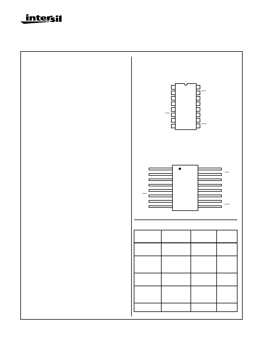
Pinouts
16 LEAD CERAMIC DUAL-IN-LINE
METAL SEAL PACKAGE (SBDIP)
MIL-STD-1835 CDIP2-T16, LEAD FINISH C
TOP VIEW
16 LEAD CERAMIC METAL SEAL
FLATPACK PACKAGE (FLATPACK)
MIL-STD-1835 CDFP4-F16, LEAD FINISH C
TOP VIEW
Ordering Information
PART
NUMBER
TEMPERATURE
RANGE
SCREENING
LEVEL
PACKAGE
HCS166DMSR
-55
o
C to +125
o
C
Intersil Class S
Equivalent
16 Lead
SBDIP
HCS166KMSR
-55
o
C to +125
o
C
Intersil Class S
Equivalent
16 Lead
Ceramic
Flatpack
HCS166D/
Sample
+25
o
C
Sample
16 Lead
SBDIP
HCS166K/
Sample
+25
o
C
Sample
16 Lead
Ceramic
Flatpack
HCS166HMSR
+25
o
C
Die
Die
14
15
16
9
13
12
11
10
1
2
3
4
5
7
6
8
D0
D1
D2
D3
CE
GND
CP
D7
Q7
D6
D5
D4
PE
DS
VCC
MR
2
3
4
5
6
7
8
1
16
15
14
13
12
11
10
9
D0
D1
D2
D3
CE
GND
CP
DS
D7
Q7
D6
D5
D4
PE
VCC
MR
Features
∑ 3 Micron Radiation Hardened CMOS SOS
∑ Total Dose 200K RAD (Si)
∑ SEP Effective LET No Upsets: >100 MEV-cm
2
/mg
∑ Single Event Upset (SEU) Immunity < 2 x 10
-9
Errors/
Bit-Day (Typ)
∑ Dose Rate Survivability: >1 x 10
12
RAD (Si)/s
∑ Dose Rate Upset >10
10
RAD s(Si)/s 20ns Pulse
∑ Latch-Up Free Under Any Conditions
∑ Fanout (Over Temperature Range)
- Standard Outputs - 10 LSTTL Loads
∑ Military Temperature Range: -55
o
C to +125
o
C
∑ Significant Power Reduction Compared to LSTTL ICs
∑ DC Operating Voltage Range: 4.5V to 5.5V
∑ Input Logic Levels
- VIL = 0.3 VCC Max
- VIH = 0.7 VCC Min
∑ Input Current Levels Ii
5
µ
A at VOL, VOH
Description
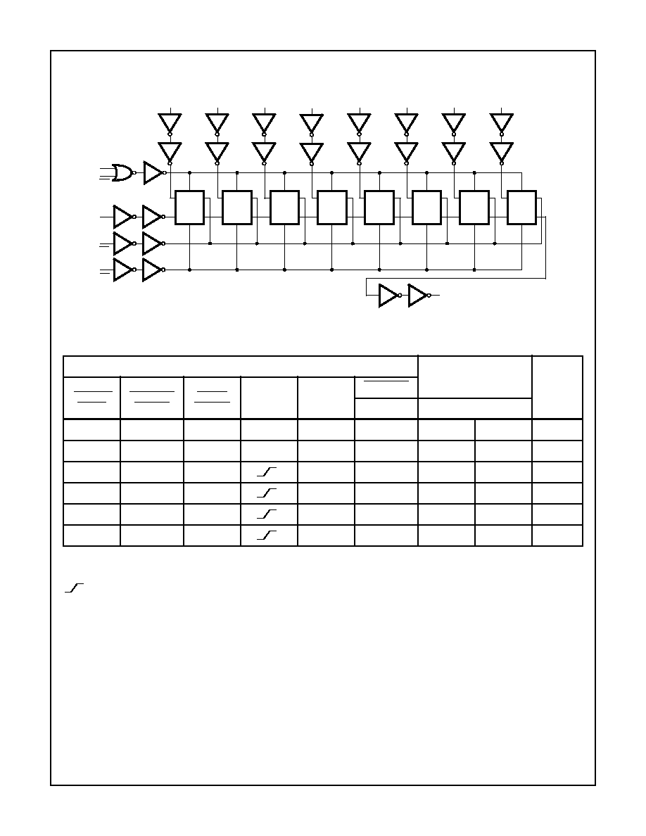
The Intersil HCS166MS is an 8-bit shift register that has fully
synchronous serial or parallel data entry selected by an
active LOW Parallel Enable (PE) input. When the PE is LOW
one setup time before the LOW-to-HIGH clock transition,
parallel data is entered into the register. When PE is HIGH,
data is entered into internal bit position Q0 from Serial Data
Input (DS), and the remaining bits are shifted one place to
the right (Q0
Q1
Q2m etc.) with each positive-going
clock transition. For expansion of the register in parallel to
serial converters, the Q7 output is connected to the DS input
of the succeeding stage.
The clock input is a gated OR structure which allows one
input to be used as an active LOW Clock Enable (CE) input.
The pin assignment for the CP and CE inputs is arbitrary and
con be reversed for layout convenience. The LOW-to-HIGH
transition of CE input should only take place while the CP is
HIGH for predictable operation.
A LOW on the Master Reset (MR) input overrides all other
inputs and clears the register asynchronously, forcing all bit
positions to a LOW state.
The HCS166MS utilizes advanced CMOS/SOS technology
to achieve high-speed operation. This device is a member of
radiation hardened, high-speed, CMOS/SOS Logic Family.
The HCS166MS is supplied in a 16 lead Ceramic flatpack
(K suffix) or a SBDIP Package (D suffix).
Spec Number
518758
File Number
2482.2
September 1995
251
HCS166MS
Functional Diagram
TRUTH TABLE
INPUTS
INTERNAL Q STATES
OUTPUT
Q7
MASTER
RESET
PARALLEL
ENABLE
CLOCK
ENABLE
CLOCK
SERIAL
PARALLEL
D0 - D7
Q0 Q1
L
X
X
X
X
X
L
L
L
H
X
L
L
X
X
Q00
Q10
Q0
H
L
L
X
a . . . h
a
b
h
H
H
L
H
X
H
Q0n
Q6n
H
H
L
L
X
L
Q0n
Q6n
H
X
H
X
X
Q00
Q10
Q70
H = High Level
L = Low Level
X = Immaterial
= Transition from low to high level
a . . . h = The level of steady state input at inputs D0 thru D7, respectively.
Q00, Q10, Q70 = The level of Q0, Q1, or Q7, respectively, before the indicated steady
state input conditions were established.
Q0n, Q6n = the level of Q0 or Q6, respectively, before the most recent transition of the
clock.
MR
CE
DS
PE
CP
Q7
D2
D0
D3
D5
D6
D7
D4
D1
Spec Number
518758

252
Specifications HCS166MS
Absolute Maximum Ratings
Reliability Information
Supply Voltage . . . . . . . . . . . . . . . . . . . . . . . . . . . . . . -0.5V to +7.0V
Input Voltage Range, All Inputs . . . . . . . . . . . . .-0.5V to VCC +0.5V
DC Input Current, Any One Input
. . . . . . . . . . . . . . . . . . . . . . . .±
10mA
DC Drain Current, Any One Output
. . . . . . . . . . . . . . . . . . . . . . .±
25mA
(All Voltage Reference to the VSS Terminal)
Storage Temperature Range (TSTG) . . . . . . . . . . . -65
o
C to +150
o
C
Lead Temperature (Soldering 10sec) . . . . . . . . . . . . . . . . . . +265
o
C
Junction Temperature (TJ) . . . . . . . . . . . . . . . . . . . . . . . . . . +175
o
C
ESD Classification . . . . . . . . . . . . . . . . . . . . . . . . . . . . . . . . Class 1
Thermal Resistance
JA
JC
SBDIP Package. . . . . . . . . . . . . . . . . . . .
73
o
C/W
24
o
C/W
Ceramic Flatpack Package . . . . . . . . . . .
114
o
C/W
29
o
C/W
Maximum Package Power Dissipation at +125
o
C Ambient
SBDIP Package. . . . . . . . . . . . . . . . . . . . . . . . . . . . . . . . . . 0.68W
Ceramic Flatpack Package . . . . . . . . . . . . . . . . . . . . . . . . . 0.44W
If device power exceeds package dissipation capability, provide heat
sinking or derate linearly at the following rate:
SBDIP Package. . . . . . . . . . . . . . . . . . . . . . . . . . . . . . 13.7mW/
o
C
Ceramic Flatpack Package . . . . . . . . . . . . . . . . . . . . . . 8.8mW/
o
C
CAUTION: As with all semiconductors, stress listed under "Absolute Maximum Ratings" may be applied to devices (one at a time) without resulting in permanent
damage. This is a stress rating only. Exposure to absolute maximum rating conditions for extended periods may affect device reliability. The conditions listed
under "Electrical Performance Characteristics" are the only conditions recommended for satisfactory device operation.
Operating Conditions
Supply Voltage . . . . . . . . . . . . . . . . . . . . . . . . . . . . . +4.5V to +5.5V
Input Rise and Fall Times at 4.5V VCC (TR, TF) . . . . . . .500ns Max
Operating Temperature Range (T
A
) . . . . . . . . . . . . -55
o
C to +125
o
C
Input Low Voltage (VIL). . . . . . . . . . . . . . . . . . . 0.0V to 30% of VCC
Input High Voltage (VIH) . . . . . . . . . . . . . . . . . . 70% of VCC to VCC
TABLE 1. DC ELECTRICAL PERFORMANCE CHARACTERISTICS
PARAMETER
SYMBOL
(NOTE 1)
CONDITIONS
GROUP
A SUB-
GROUPS
TEMPERATURE
LIMITS
UNITS
MIN
MAX
Quiescent Current
ICC
VCC = 5.5V,
VIN = VCC or GND
1
+25
o
C
-
40
µ
A
2, 3
+125
o
C, -55
o
C
-
750
µ
A
Output Current
(Sink)
IOL
VCC = 4.5V, VIH = 4.5V,
VOUT = 0.4V, VIL = 0V
1
+25
o
C
4.8
-
mA
2, 3
+125
o
C, -55
o
C
4.0
-
mA
Output Current
(Source)
IOH
VCC = 4.5V, VIH = 4.5V,
VOUT = VCC -0.4V,
VIL = 0V
1
+25
o
C
-4.8
-
mA
2, 3
+125
o
C, -55
o
C
-4.0
-
mA
Output Voltage Low
VOL
VCC = 4.5V, VIH = 3.15V,
IOL = 50
µ
A, VIL = 1.35V
1, 2, 3
+25
o
C, +125
o
C, -55
o
C
-
0.1
V
VCC = 5.5V, VIH = 3.85V,
IOL = 50
µ
A, VIL = 1.65V
1, 2, 3
+25
o
C, +125
o
C, -55
o
C
-
0.1
V
Output Voltage High
VOH
VCC = 4.5V, VIH = 3.15V,
IOH = -50
µ
A, VIL = 1.35V
1, 2, 3
+25
o
C, +125
o
C, -55
o
C
VCC
-0.1
-
V
VCC = 5.5V, VIH = 3.85V,
IOH = -50
µ
A, VIL = 1.65V
1, 2, 3
+25
o
C, +125
o
C, -55
o
C
VCC
-0.1
-
V
Input Leakage
Current
IIN
VCC = 5.5V, VIN = VCC or
GND
1
+25
o
C
-
±
0.5
µ
A
2, 3
+125
o
C, -55
o
C
-
±
5.0
µ
A
Noise Immunity
Functional Test
FN
VCC = 4.5V,
VIH = 0.70(VCC),
VIL = 0.30(VCC), (Note 2)
7, 8A, 8B
+25
o
C, +125
o
C, -55
o
C
-
-
-
NOTES:
1. All voltages reference to device GND.
2. For functional tests, VO
4.0V is recognized as a logic "1", and VO
0.5V is recognized as a logic "0".
Spec Number
518758

253
Specifications HCS166MS
TABLE 2. AC ELECTRICAL PERFORMANCE CHARACTERISTICS
PARAMETER
SYMBOL
(NOTES 1, 2)
CONDITIONS
GROUP
A SUB-
GROUPS
TEMPERATURE
LIMITS
UNITS
MIN
MAX
CP or CE to Q7
TPHL
TPLH
VCC = 4.5V
9
+25
o
C
2
32
ns
10, 11
+125
o
C, -55
o
C
2
37
ns
MR to Q7
TPHL
VCC = 4.5V
9
+25
o
C
2
31
ns
10, 11
+125
o
C, -55
o
C
2
36
ns
NOTES:
1. All voltages referenced to device GND.
2. AC measurements assume RL = 500
, CL = 50pF, Input TR = TF = 3ns, VIL = GND, VIH = VCC.
TABLE 3. ELECTRICAL PERFORMANCE CHARACTERISTICS
PARAMETER
SYMBOL
(NOTE 1)
CONDITIONS
TEMPERATURE
LIMITS
UNITS
MIN
MAX
Capacitance Power Dissipation
CPD
VCC = 5.0V, f = 1MHz
+25
o
C
-
65
pF
+125
o
C, -55
o
C
-
81
pF
Input Capacitance
CIN
VCC = 5.0V, f = 1MHz
+25
o
C
-
10
pF
+125
o
C
-
10
pF
Output Transition Time
(Figure 1)
TTHL
TTLH
VCC = 4.5V
+25
o
C
-
15
ns
+125
o
C, -55
o
C
-
22
ns
Clock Frequency (Figure 1)
fmax
VCC = 4.5V
+25
o
C
30
-
MHz
-55
o
C to +125
o
C
20
-
MHz
MR Pulse Width (Figure 2)
tw
VCC = 4.5V
+25
o
C
20
-
ns
-55
o
C to +125
o
C
30
-
ns
Clock Pulse Width (Figure 1)
tw
VCC = 4.5V
+25
o
C
16
-
ns
-55
o
C to +125
o
C
24
-
ns
Set-up Time Data and CE to
Clock, (Figure 3, 4)
tSU
VCC = 4.5V
+25
o
C
16
-
ns
-55
o
C to +125
o
C
24
-
ns
Hold Time Data to Clock
(Figure 4)
tH
VCC = 4.5V
+25
o
C
1
-
ns
-55
o
C to +125
o
C
1
-
ns
Removal Time MR to Clock
(Figure 3)
tREM
VCC = 4.5V
+25
o
C
0
-
ns
-55
o
C to +125
o
C
0
-
ns
Set-up Time PE to CP (Figure 4)
tSU
VCC = 4.5V
+25
o
C
29
-
ns
-55
o
C to +125
o
C
44
-
ns
Hold Time PE to CP or CE
(Figure 4)
tH
VCC = 4.5V
+25
o
C
0
-
ns
-55
o
C to +125
o
C
0
-
ns
NOTE:
1. The parameters listed in Table 3 are controlled via design or process parameters. Min and Max Limits are guaranteed but not directly
tested. These parameters are characterized upon initial design release and upon design changes which affect these characteristics.
Spec Number
518758
254
Specifications HCS166MS
TABLE 4. DC POST RADIATION ELECTRICAL PERFORMANCE CHARACTERISTICS
PARAMETER
SYMBOL
(NOTES 1, 2)
CONDITIONS
TEMPERATURE
200K RAD
LIMITS
UNITS
MIN
MAX
Quiescent Current
ICC
VCC = 5.5V, VIN = VCC or GND
+25
o
C
-
0.75
mA
Output Current (Sink)
IOL
VCC = 4.5V, VIN = VCC or GND,
VOUT = 0.4V
+25
o
C
4.0
-
mA
Output Current
(Source)
IOH
VCC = 4.5V, VIN = VCC or GND,
VOUT = VCC -0.4V
+25
o
C
-4.0
-
mA
Output Voltage Low
VOL
VCC = 4.5V and 5.5V, VIH = 0.70(VCC),
VIL = 0.30(VCC), IOL = 50
µ
A
+25
o
C
-
0.1
V
Output Voltage High
VOH
VCC = 4.5V and 5.5V, VIH = 0.70(VCC),
VIL = 0.30(VCC), IOH = -50
µ
A
+25
o
C
VCC
-0.1
-
V
Input Leakage Current
IIN
VCC = 5.5V, VIN = VCC or GND
+25
o
C
-
±
5
µ
A
Noise Immunity
Functional Test
FN
VCC = 4.5V, VIH = 0.70(VCC),
VIL = 0.30(VCC), (Note 3)
+25
o
C
-
-
-
CP or CE to Q7
TPHL
VCC = 4.5V
+25
o
C
2
37
ns
TPLH
VCC = 4.5V
+25
o
C
2
37
ns
MR to Q7
TPHL
VCC = 4.5V
+25
o
C
2
36
ns
NOTES:
1. All voltages referenced to device GND.
2. AC measurements assume RL = 500
, CL = 50pF, Input TR = TF = 3ns, VIL = GND, VIH = VCC.
3. For functional tests, VO
4.0V is recognized as a logic "1", and VO
0.5V is recognized as a logic "0".
TABLE 5. BURN-IN AND OPERATING LIFE TEST, DELTA PARAMETERS (+25
o
C)
PARAMETER
GROUP B
SUBGROUP
DELTA LIMIT
ICC
5
12
µ
A
IOL/IOH
5
-15% of 0 Hour
Spec Number
518758