324
CAUTION: These devices are sensitive to electrostatic discharge; follow proper IC Handling Procedures.
1-888-INTERSIL or 321-724-7143 | Copyright © Intersil Corporation 1999
Ordering Information
PART NUMBER
TEMPERATURE RANGE
SCREENING LEVEL
PACKAGE
HCS573DMSR
-55
o
C to +125
o
C
Intersil Class S Equivalent
20 Lead SBDIP
HCS573KMSR
-55
o
C to +125
o
C
Intersil Class S Equivalent
20 Lead Ceramic Flatpack
HCS573D/Sample
+25
o
C
Sample
20 Lead SBDIP
HCS573K/Sample
+25
o
C
Sample
20 Lead Ceramic Flatpack
HCS573HMSR
+25
o
C
Die
Die
HCS573MS
Radiation Hardened
Octal Transparent Latch, Three-State
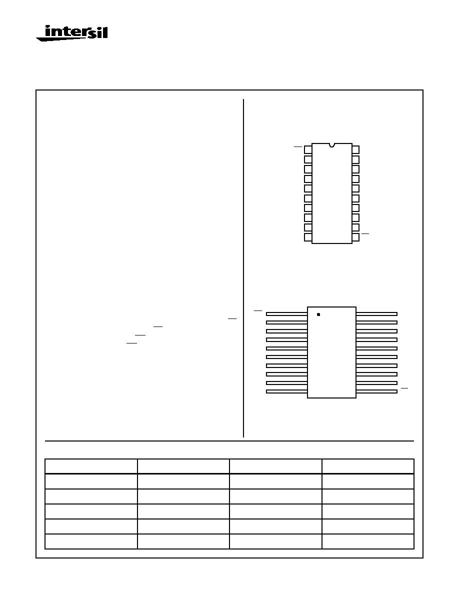
Pinouts
20 LEAD CERAMIC DUAL-IN-LINE
METAL SEAL PACKAGE (SBDIP)
MIL-STD-1835 CDIP2-T20, LEAD FINISH C
TOP VIEW
20 LEAD CERAMIC METAL SEAL
FLATPACK PACKAGE (FLATPACK)
MIL-STD-1835 CDFP4-F20, LEAD FINISH C
TOP VIEW
11
12
13
14
15
16
17
18
20
19
10
9
8
7
6
5
4
3
2
1
OE
D0
D1
D2
D3
D4
D6
D5
D7
GND
VCC
Q1
Q2
Q3
Q0
Q4
Q5
Q6
Q7
LE
2
3
4
5
6
7
8
1
20
19
18
17
16
15
14
13
OE
D0
D1
D2
D3
D4
D5
D6
9
10
12
11
D7
GND
VCC
Q0
Q1
Q2
Q3
Q4
Q5
Q6
Q7
LE
Features
∑ 3 Micron Radiation Hardened SOS CMOS
∑ Total Dose 200K RAD (Si)
∑ SEP Effective LET No Upsets: >100 MEV-cm
2
/mg
∑ Single Event Upset (SEU) Immunity < 2 x 10
-9
Errors/Bit-
Day (Typ)
∑ Dose Rate Survivability: >1 x 10
12
RAD (Si)/s
∑ Dose Rate Upset >10
10
RAD (Si)/s 20ns Pulse
∑ Latch-Up Free Under Any Conditions
∑ Fanout (Over Temperature Range)
- Bus Driver Outputs - 15 LSTTL Loads
∑ Military Temperature Range: -55
o
C to +125
o
C
∑ Significant Power Reduction Compared to LSTTL ICs
∑ DC Operating Voltage Range: 4.5V to 5.5V
∑ Input Logic Levels
- VIL = 0.3 VCC Max
- VIH = 0.7 VCC Min
∑ Input Current Levels Ii
5
µ
A at VOL, VOH
Description
The Intersil HCS573MS is a Radiation Hardened octal transpar-
ent three-state latch with an active low output enable. The
HCS573MS utilizes advanced CMOS/SOS technology. The
outputs are transparent to the inputs when the Latch Enable (LE)
is HIGH. When the Latch Enable (LE) goes LOW, the data is
latched. The Output Enable (OE) controls the tri-state outputs.
When the Output Enable (OE) is HIGH, the outputs are in the
high impedance state. The latch operation is independent of the
state of the Output Enable.
The HCS573MS utilizes advanced CMOS/SOS technology to
achieve high-speed operation. This device is a member of
radiation hardened, high-speed, CMOS/SOS Logic Family.
The HCS573MS is supplied in a 20 lead Ceramic flatpack
(K suffix) or a SBDIP Package (D suffix).
September 1995
Spec Number
518771
File Number
4056
325
HCS573MS
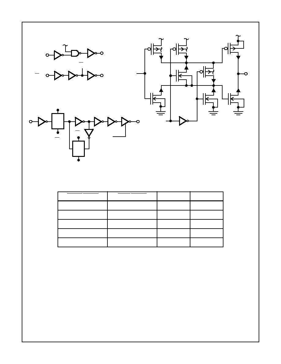
Functional Diagram
TRUTH TABLE
OUTPUT ENABLE
LATCH ENABLE
DATA
OUTPUT
L
H
H
H
L
H
L
L
L
L
I
L
L
L
h
H
H
X
X
Z
H = High Level
L = Low Level
X = Immaterial
Z = High Impedance
I = Low voltage level prior to the high-to-low latch enable transition
h = High voltage level prior to the high-to-low latch enable transition
OE
LE
LE
LE
OE
P
P
N
A
OE
P
N
P
Qn
N
N
LE
LE
P
N
Dn
Qn
OE
A
P
N
LE
LE
Spec Number
518771
326
Specifications HCS573MS
Absolute Maximum Ratings
Reliability Information
Supply Voltage (VCC). . . . . . . . . . . . . . . . . . . . . . . . . -0.5V to +7.0V
Input Voltage Range, All Inputs . . . . . . . . . . . . .-0.5V to VCC +0.5V
DC Input Current, Any One Input
. . . . . . . . . . . . . . . . . . . . . . . .±
10mA
DC Drain Current, Any One Output
. . . . . . . . . . . . . . . . . . . . . . .±
25mA
(All Voltage Reference to the VSS Terminal)
Storage Temperature Range (TSTG) . . . . . . . . . . . -65
o
C to +150
o
C
Lead Temperature (Soldering 10sec) . . . . . . . . . . . . . . . . . . +265
o
C
Junction Temperature (TJ) . . . . . . . . . . . . . . . . . . . . . . . . . . +175
o
C
ESD Classification . . . . . . . . . . . . . . . . . . . . . . . . . . . . . . . . Class 1
Thermal Resistance
JA
JC
SBDIP Package. . . . . . . . . . . . . . . . . . . .
72
o
C/W
24
o
C/W
Ceramic Flatpack Package . . . . . . . . . . .
107
o
C/W
28
o
C/W
Maximum Package Power Dissipation at +125
o
C Ambient
SBDIP Package. . . . . . . . . . . . . . . . . . . . . . . . . . . . . . . . . . 0.69W
Ceramic Flatpack Package . . . . . . . . . . . . . . . . . . . . . . . . . 0.47W
If device power exceeds package dissipation capability, provide heat
sinking or derate linearly at the following rate:
SBDIP Package. . . . . . . . . . . . . . . . . . . . . . . . . . . . . . 13.9mW/
o
C
Ceramic Flatpack Package . . . . . . . . . . . . . . . . . . . . . . 9.3mW/
o
C
CAUTION: As with all semiconductors, stress listed under "Absolute Maximum Ratings" may be applied to devices (one at a time) without resulting in permanent
damage. This is a stress rating only. Exposure to absolute maximum rating conditions for extended periods may affect device reliability. The conditions listed
under "Electrical Performance Characteristics" are the only conditions recommended for satisfactory device operation..
Operating Conditions
Supply Voltage (VCC). . . . . . . . . . . . . . . . . . . . . . . . +4.5V to +5.5V
Input Rise and Fall Times at VCC = 4.5V (TR, TF) . . . . .500ns Max
Operating Temperature Range (T
A
) . . . . . . . . . . . . -55
o
C to +125
o
C
Input Low Voltage (VIL). . . . . . . . . . . . . . . . . . . 0.0V to 30% of VCC
Input High Voltage (VIH) . . . . . . . . . . . . . . . . . . 70% of VCC to VCC
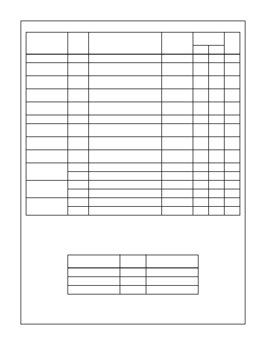
TABLE 1. DC ELECTRICAL PERFORMANCE CHARACTERISTICS
PARAMETER
SYMBOL
(NOTE 1)
CONDITIONS
GROUP
A SUB-
GROUPS
TEMPERATURE
LIMITS
UNITS
MIN
MAX
Quiescent Current
ICC
VCC = 5.5V,
VIN = VCC or GND
1
+25
o
C
-
40
µ
A
2, 3
+125
o
C, -55
o
C
-
750
µ
A
Output Current
(Sink)
IOL
VCC = 4.5V, VIH = 4.5V,
VOUT = 0.4V, VIL = 0V
1
+25
o
C
7.2
-
mA
2, 3
+125
o
C, -55
o
C
6.0
-
mA
Output Current
(Source)
IOH
VCC = 4.5V, VIH = 4.5V,
VOUT = VCC -0.4V,
VIL = 0V
1
+25
o
C
-7.2
-
mA
2, 3
+125
o
C, -55
o
C
-6.0
-
mA
Output Voltage Low
VOL
VCC = 4.5V, VIH = 3.15V,
IOL = 50
µ
A, VIL = 1.35V
1, 2, 3
+25
o
C, +125
o
C, -55
o
C
-
0.1
V
VCC = 5.5V, VIH = 3.85V,
IOL = 50
µ
A, VIL = 1.65V
1, 2, 3
+25
o
C, +125
o
C, -55
o
C
-
0.1
V
Output Voltage High
VOH
VCC = 4.5V, VIH = 3.15V,
IOH = -50
µ
A, VIL = 1.35V
1, 2, 3
+25
o
C, +125
o
C, -55
o
C
VCC
-0.1
-
V
VCC = 5.5V, VIH = 3.85V,
IOH = -50
µ
A, VIL = 1.65V
1, 2, 3
+25
o
C, +125
o
C, -55
o
C
VCC
-0.1
-
V
Input Leakage
Current
IIN
VCC = 5.5V, VIN = VCC or
GND
1
+25
o
C
-
±
0.5
µ
A
2, 3
+125
o
C, -55
o
C
-
±
5.0
µ
A
Output Leakage
Current
IOZ
VCC = 5.5V, VIN = 0V or
VCC
1
+25
o
C
-
±1.0
µ
A
2, 3
+125
o
C, -55
o
C
-
±50
µ
A
Noise Immunity
Functional Test
FN
VCC = 4.5V,
VIH = 0.70(VCC),
VIL = 0.30(VCC) (Note 2)
7, 8A, 8B
+25
o
C, +125
o
C, -55
o
C
-
-
-
NOTES:
1. All voltages reference to device GND.
2. For functional tests VO
4.0V is recognized as a logic "1", and VO
0.5V is recognized as a logic "0".
Spec Number
518771
327
Specifications HCS573MS
TABLE 2. AC ELECTRICAL PERFORMANCE CHARACTERISTICS
PARAMETER
SYMBOL
(NOTES 1, 2)
CONDITIONS
GROUP
A SUB-
GROUPS
TEMPERATURE
LIMITS
UNITS
MIN
MAX
Data to Qn
TPLH
TPHL
VCC = 4.5V
9
+25
o
C
2
24
ns
10, 11
+125
o
C, -55
o
C
2
29
ns
LE to Qn
TPLH
VCC = 4.5V
9
+25
o
C
2
27
ns
10, 11
+125
o
C, -55
o
C
2
35
ns
TPHL
VCC = 4.5V
9
+25
o
C
2
31
ns
10, 11
+125
o
C, -55
o
C
2
40
ns
Enable to Output
TPZL
VCC = 4.5V
9
+25
o
C
2
27
ns
10, 11
+125
o
C, -55
o
C
2
33
ns
TPZH
VCC = 4.5V
9
+25
o
C
2
24
ns
10, 11
+125
o
C, -55
o
C
2
29
ns
Disable to Output
TPLZ
VCC = 4.5V
9
+25
o
C
2
25
ns
10, 11
+125
o
C, -55
o
C
2
29
ns
TPHZ
VCC = 4.5V
9
+25
o
C
2
21
ns
10, 11
+125
o
C, -55
o
C
2
25
ns
NOTES:
1. All voltages referenced to device GND.
2. AC measurements assume RL = 500
, CL = 50pF, Input TR = TF = 3ns, VIL = GND, VIH = VCC.
TABLE 3. ELECTRICAL PERFORMANCE CHARACTERISTICS
PARAMETER
SYMBOL
CONDITIONS
NOTES
TEMPERATURE
LIMITS
UNITS
MIN
MAX
Capacitance Power
Dissipation
CPD
VCC = 5.0V, f = 1MHz
1
+25
o
C
-
30
pF
1
+125
o
C, -55
o
C
-
60
pF
Input Capacitance
CIN
VCC = 5.0V, f = 1MHz
1
+25
o
C
-
10
pF
1
+125
o
C, -55
o
C
-
10
pF
Output Transition
Time
TTHL
TTLH
VCC = 4.5V
1
+25
o
C
-
12
ns
1
+125
o
C, -55
o
C
-
18
ns
Setup Time Data to
LE
TSU
VCC = 4.5V
1
+25
o
C
10
-
ns
1
+125
o
C, -55
o
C
15
-
ns
Hold Time Data to
LE
TH
VCC = 4.5V
1
+25
o
C
8
-
ns
1
+125
o
C, -55
o
C
12
-
ns
Pulse Width LE
TW
VCC = 4.5V
1
+25
o
C
16
-
ns
1
+125
o
C, -55
o
C
24
-
ns
NOTE:
1. The parameters listed in Table 3 are controlled via design or process parameters. Min and Max Limits are guaranteed but not directly
tested. These parameters are characterized upon initial design release and upon design changes which affect these characteristics.
Spec Number
518771
328
Specifications HCS573MS
TABLE 4. DC POST RADIATION ELECTRICAL PERFORMANCE CHARACTERISTICS
PARAMETER
SYMBOL
(NOTES 1, 2)
CONDITIONS
TEMPERATURE
200K RAD
LIMITS
UNITS
MIN
MAX
Quiescent Current
ICC
VCC = 5.5V, VIN = VCC or GND
+25
o
C
-
0.75
mA
Output Current (Sink)
IOL
VCC = 4.5V, VIN = VCC or GND,
VOUT = 0.4V
+25
o
C
6.0
-
mA
Output Current
(Source)
IOH
VCC = 4.5V, VIN = VCC or GND,
VOUT = VCC -0.4V
+25
o
C
-6.0
-
mA
Output Voltage Low
VOL
VCC = 4.5V or 5.5V, VIH = 0.70(VCC),
VIL = 0.30(VCC), IOL = 50
µ
A
+25
o
C
-
0.1
V
Output Voltage High
VOH
VCC = 4.5V or 5.5V, VIH = 0.70(VCC),
VIL = 0.30(VCC), IOH = -50
µ
A
+25
o
C
VCC
-0.1
-
V
Input Leakage Current
IIN
VCC = 5.5V, VIN = VCC or GND
+25
o
C
-
±
5
µ
A
Tri-State Output
Leakage Current
IOZ
Applied Voltage = 0V or VCC, VCC = 5.5V
+25
o
C
-
±
50
µ
A
Noise Immunity
Functional Test
FN
VCC = 4.5V, VIH = 0.70(VCC),
VIL = 0.30(VCC), (Note 3)
+25
o
C
-
-
-
Data to Qn
TPHL
TPLH
VCC = 4.5V
+25
o
C
2
29
ns
LEN to Qn
TPLH
VCC = 4.5V
+25
o
C
2
35
ns
TPHL
VCC = 4.5V
+25
o
C
2
40
ns
Enable to Output
TPZL
VCC = 4.5V
+25
o
C
2
33
ns
TPZH
VCC = 4.5V
+25
o
C
2
29
ns
Disable to Output
TPLZ
VCC = 4.5V
+25
o
C
2
29
ns
TPHZ
VCC = 4.5V
+25
o
C
2
25
ns
NOTES:
1. All voltages referenced to device GND.
2. AC measurements assume RL = 500
, CL = 50pF, Input TR = TF = 3ns, VIL = GND, VIH = VCC.
3. For functional tests VO
4.0V is recognized as a logic "1", and VO
0.5V is recognized as a logic "0".
TABLE 5. BURN-IN AND OPERATING LIFE TEST, DELTA PARAMETERS (+25
o
C)
PARAMETER
GROUP B
SUBGROUP
DELTA LIMIT
ICC
5
12
µ
A
IOL/IOH
5
-15% of 0 Hour
IOZL/IOZH
5
±
200nA
Spec Number
518771
329
Specifications HCS573MS
TABLE 6. APPLICABLE SUBGROUPS
CONFORMANCE GROUPS
METHOD
GROUP A SUBGROUPS
READ AND RECORD
Initial Test (Preburn-In)
100%/5004
1, 7, 9
ICC, IOL/H
Interim Test
I
(Postburn-In)
100%/5004
1, 7, 9
ICC, IOL/H
Interim Test
II
(Postburn-In)
100%/5004
1, 7, 9
ICC, IOL/H
PDA
100%/5004
1, 7, 9, Deltas
Interim Test
III
(Postburn-In)
100%/5004
1, 7, 9
ICC, IOL/H
PDA
100%/5004
1, 7, 9, Deltas
Final Test
100%/5004
2, 3, 8A, 8B, 10, 11
Group A (Note 1)
Sample/5005
1, 2, 3, 7, 8A, 8B, 9, 10, 11
Group B
Subgroup B-5
Sample/5005
1, 2, 3, 7, 8A, 8B, 9, 10, 11, Deltas
Subgroups 1, 2, 3, 9, 10, 11,
(Note 2)
Subgroup B-6
Sample/5005
1, 7, 9
Group D
Sample/5005
1, 7, 9
NOTES:
1. Alternate Group A testing in accordance with method 5005 of MIL-STD-883 may be exercised.
2. Table 5 parameters only.
TABLE 7. TOTAL DOSE IRRADIATION
CONFORMANCE
GROUPS
METHOD
TEST
READ AND RECORD
PRE RAD
POST RAD
PRE RAD
POST RAD
Group E Subgroup 2
5005
1, 7, 9
Table 4
1, 9
Table 4 (Note 1)
NOTE:
1. Except FN test which will be performed 100% Go/No-Go.
TABLE 8. STATIC AND DYNAMIC BURN-IN TEST CONNECTIONS
OPEN
GROUND
1/2 VCC = 3V
±
0.5V
VCC = 6V
±
0.5V
OSCILLATOR
50kHz
25kHz
STATIC BURN-IN I TEST CONNECTIONS (Note 1)
12 - 19
1 - 11
-
20
-
-
STATIC BURN-IN II TEST CONNECTIONS (Note 1)
12 - 19
10
-
1 - 9, 11, 20
-
-
DYNAMIC BURN-IN TEST CONNECTIONS (Note 2)
-
1, 10
12 - 19
20
11
2 - 9
NOTES:
1. Each pin except VCC and GND will have a resistor of 10k
±
5% for static burn-in
2. Each pin except VCC and GND will have a resistor of 680
±
5% for dynamic burn-in
TABLE 9. IRRADIATION TEST CONNECTIONS
OPEN
GROUND
VCC = 5V
±
0.5V
12 - 19
10
1 - 9, 11, 20
NOTE: Each pin except VCC and GND will have a resistor of 47K
±
5% for irradiation testing.
Group E, Subgroup 2, sample size is 4 dice/wafer 0 failures.
Spec Number
518771

330
All Intersil semiconductor products are manufactured, assembled and tested under ISO9000 quality systems certification.
Intersil products are sold by description only. Intersil Corporation reserves the right to make changes in circuit design and/or specifications at any time without
notice. Accordingly, the reader is cautioned to verify that data sheets are current before placing orders. Information furnished by Intersil is believed to be accurate
and reliable. However, no responsibility is assumed by Intersil or its subsidiaries for its use; nor for any infringements of patents or other rights of third parties which
may result from its use. No license is granted by implication or otherwise under any patent or patent rights of Intersil or its subsidiaries.
For information regarding Intersil Corporation and its products, see web site http://www.intersil.com
HCS573MS
Intersil Space Level Product Flow - `MS'
Wafer Lot Acceptance (All Lots) Method 5007
(Includes SEM)
GAMMA Radiation Verification (Each Wafer) Method 1019,
4 Samples/Wafer, 0 Rejects
100% Nondestructive Bond Pull, Method 2023
Sample - Wire Bond Pull Monitor, Method 2011
Sample - Die Shear Monitor, Method 2019 or 2027
100% Internal Visual Inspection, Method 2010, Condition A
100% Temperature Cycle, Method 1010, Condition C,
10 Cycles
100% Constant Acceleration, Method 2001, Condition per
Method 5004
100% PIND, Method 2020, Condition A
100% External Visual
100% Serialization
100% Initial Electrical Test (T0)
100% Static Burn-In 1, Condition A or B, 24 hrs. min.,
+125
o
C min., Method 1015
100% Interim Electrical Test 1 (T1)
100% Delta Calculation (T0-T1)
100% Static Burn-In 2, Condition A or B, 24 hrs. min.,
+125
o
C min., Method 1015
100% Interim Electrical Test 2 (T2)
100% Delta Calculation (T0-T2)
100% PDA 1, Method 5004 (Notes 1and 2)
100% Dynamic Burn-In, Condition D, 240 hrs., +125
o
C or
Equivalent, Method 1015
100% Interim Electrical Test 3 (T3)
100% Delta Calculation (T0-T3)
100% PDA 2, Method 5004 (Note 2)
100% Final Electrical Test
100% Fine/Gross Leak, Method 1014
100% Radiographic, Method 2012 (Note 3)
100% External Visual, Method 2009
Sample - Group A, Method 5005 (Note 4)
100% Data Package Generation (Note 5)
NOTES:
1. Failures from Interim electrical test 1 and 2 are combined for determining PDA 1.
2. Failures from subgroup 1, 7, 9 and deltas are used for calculating PDA. The maximum allowable PDA = 5% with no more than 3% of the
failures from subgroup 7.
3. Radiographic (X-Ray) inspection may be performed at any point after serialization as allowed by Method 5004.
4. Alternate Group A testing may be performed as allowed by MIL-STD-883, Method 5005.
5. Data Package Contents:
∑ Cover Sheet (Intersil Name and/or Logo, P.O. Number, Customer Part Number, Lot Date Code, Intersil Part Number, Lot Number,
Quantity).
∑ Wafer Lot Acceptance Report (Method 5007). Includes reproductions of SEM photos with percent of step coverage.
∑ GAMMA Radiation Report. Contains Cover page, disposition, Rad Dose, Lot Number, Test Package used, Specification Numbers, Test
equipment, etc. Radiation Read and Record data on file at Intersil.
∑ X-Ray report and film. Includes penetrometer measurements.
∑ Screening, Electrical, and Group A attributes (Screening attributes begin after package seal).
∑ Lot Serial Number Sheet (Good units serial number and lot number).
∑ Variables Data (All Delta operations). Data is identified by serial number. Data header includes lot number and date of test.
∑ The Certificate of Conformance is a part of the shipping invoice and is not part of the Data Book. The Certificate of Conformance is signed
by an authorized Quality Representative.
Spec Number
518771
331
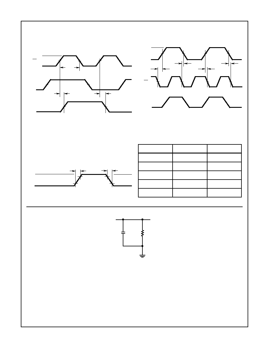
HCS573MS
AC Timing Diagrams
AC Load Circuit
FIGURE 1. LATCH ENABLE PROPAGATION DELAYS
FIGURE 2. LATCH ENABLE PREREQUISITE TIMES
FIGURE 3. DATA SET-UP AND HOLD TIMES
LE
DATA
VS
TW
VS
VS
VS
INPUT
LEVEL
VS
TPLH
VS
QN
VS
TPHL
TSU(H)
TH(H)
TSU(L)
TH(L)
INPUT
DATA
LE
LEVEL
QN
VS
VS
VS
VS
VS
VS
OUTPUT
TTHL
80%
20%
80%
20%
VOH
VOL
TTLH
AC VOLTAGE LEVELS
PARAMETER
HCS
UNITS
VCC
4.50
V
VIH
4.50
V
VS
2.25
V
VIL
0
V
GND
0
V
DUT
TEST
CL
RL
POINT
CL = 50pF
RL = 500
Spec Number
518771
332
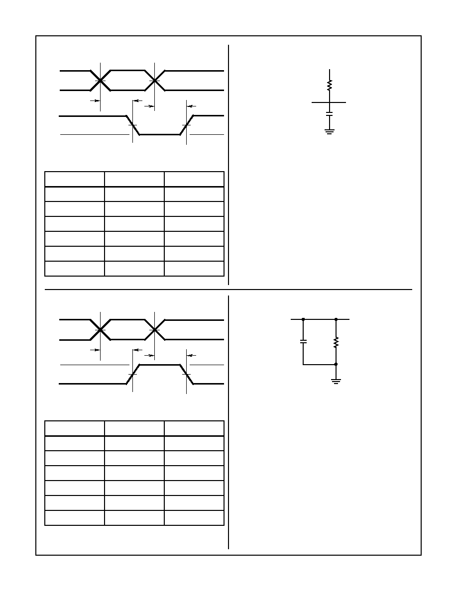
HCS573MS
Three-State Low Timing Diagram
THREE-STATE LOW VOLTAGE LEVELS
PARAMETER
HCS
UNITS
VCC
4.50
V
VIH
4.50
V
VS
2.25
V
VT
2.25
V
VW
0.90
V
GND
0
V
VS
INPUT
OUTPUT
VIH
VIL
VOZ
VOL
TPZL
TPLZ
VT
VW
Three-State Low Load Circuit
DUT
TEST
CL
RL
POINT
CL = 50pF
RL = 500
VCC
Spec Number
518771
Three-State HighTiming Diagram
THREE-STATE HIGH VOLTAGE LEVELS
PARAMETER
HCS
UNITS
VCC
4.50
V
VIH
4.50
V
VS
2.25
V
VT
2.25
V
VW
3.60
V
GND
0
V
VS
INPUT
OUTPUT
VIH
VIL
VOH
VOZ
TPZH
TPHZ
VT
VW
Three-State High Load Circuit
DUT
TEST
CL
RL
POINT
CL = 50pF
RL = 500
333
HCS573MS
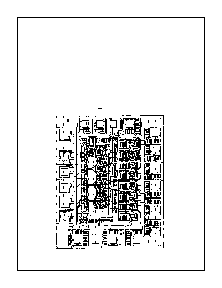
Die Characteristics
DIE DIMENSIONS:
101 x 85 mils
METALLIZATION:
Type: SiAl
Metal Thickness: 11k
≈
±
1k
≈
GLASSIVATION:
Type: SiO
2
Thickness: 13k
≈
±
2.6k
≈
WORST CASE CURRENT DENSITY:
<2.0 x 10
5
A/cm
2
BOND PAD SIZE:
100
µ
m x 100
µ
m
4 x 4 mils
Metallization Mask Layout
HCS573MS
OE
(1)
D0
(2)
VCC
(20)
Q0
(19)
D1 (3)
D3 (5)
D4 (6)
D5 (7)
(9)
(10)
D7
GND
(11)
LE
(12)
Q7
D2 (4)
D6 (8)
(18) Q1
(17) Q2
(16) Q3
(15) Q4
(14) Q5
(13) Q6
Spec Number
518771