1
CAUTION: These devices are sensitive to electrostatic discharge; follow proper IC Handling Procedures.
www.intersil.com or 407-727-9207
|
Copyright
©
Intersil Corporation 1999
Satellite Applications FlowTM (SAF) is a trademark of Intersil Corporation.
HCTS160T
Radiation Hardened Synchronous
Counter
Intersil's Satellite Applications Flow
TM
(SAF) devices are fully
tested and guaranteed to 100kRAD total dose. These QML
Class T devices are processed to a standard flow intended
to meet the cost and shorter lead-time needs of large
volume satellite manufacturers, while maintaining a high
level of reliability.
The Intersil HCTS160T is a Radiation Hardened High Speed
Presettable BCD Decade Synchronous Counter that
features an asynchronous reset and look-ahead carry logic.
Counting and parallel presetting are accomplished
synchronously with the low-to-high transition of the clock. A
low level on the synchronous parallel enable input, SPE,
disables counting and allows data at the preset inputs, P0 -
P3, to be loaded into the counter. The counter is reset by a
low on the master reset input, MR. Two count enables, PE
and TE are provided for n-bit cascading. TE also controls the
terminal count output, TC. The terminal count output
indicates a maximum count for one clock pulse and is used
to enable the next cascaded stage to count.
Specifications
Specifications for Rad Hard QML devices are controlled by
the Defense Supply Center in Columbus (DSCC). The SMD
numbers listed below must be used when ordering.
Detailed Electrical Specifications for the HCTS160T are
contained in SMD 5962-95742. A "hot-link" is provided from
our website for downloading.
www.intersil.com/spacedefense/newsafclasst.asp
Intersil`s Quality Management Plan (QM Plan), listing all
Class T screening operations, is also available on our
website.
www.intersil.com/quality/manuals.asp
Features
∑ QML Class T, Per MIL-PRF-38535
∑ Radiation Performance
- Gamma Dose (
) 1 x 10
5
RAD(Si)
- Latch-Up Free Under Any Conditions
- SEP Effective LET No Upsets: >100 MEV-cm
2
/mg
- Single Event Upset (SEU) Immunity < 2 x 10
-9
Errors/Bit-Day (Typ)
∑ 3 Micron Radiation Hardened SOS CMOS
∑ Fanout (Over Temperature Range)
- Standard Outputs 10 LSTTL Loads
∑ Significant Power Reduction Compared to LSTTL ICs
∑ DC Operating Voltage Range: 4.5V to 5.5V
∑ LSTTL Input Compatibility
- V
IL
= 0.8V Max
- V
IH
= V
CC/2
Min
∑ Input Current Levels Ii
5mA at V
OL
, V
OH
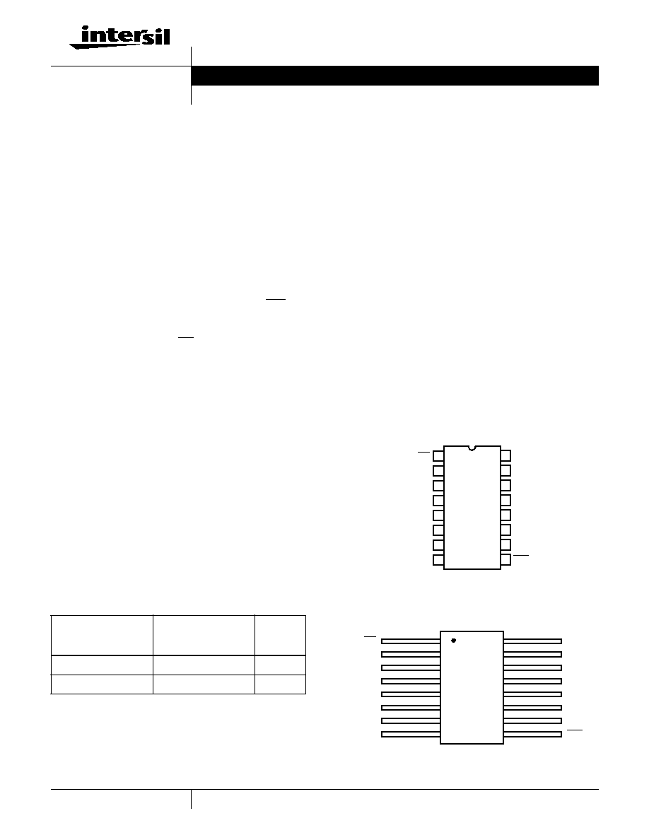
Pinouts
HCTS160DTR (SBDIP), CDIP2-T16
TOP VIEW
HCTS160KTR (FLATPACK), CDFP4-F16
TOP VIEW
Ordering Information
ORDERING
NUMBER
PART NUMBER
TEMP.
RANGE
(
o
C)
5962R9574201TEC
HCTS160DTR
-55 to 125
5962R9574201TXC
HCTS160KTR
-55 to 125
NOTE:
Minimum order quantity for -T is 150 units through
distribution, or 450 units direct.
14
15
16
9
13
12
11
10
1
2
3
4
5
7
6
8
MR
CP
P0
P1
P2
P3
GND
PE
V
CC
Q0
Q1
Q2
Q3
TE
SPE
TC
MR
CP
P0
P1
P2
P3
PE
GND
2
3
4
5
6
7
8
1
16
15
14
13
12
11
10
9
V
CC
TC
Q0
Q1
Q2
Q3
TE
SPE
Data Sheet
July 1999
File Number
4626.1
2
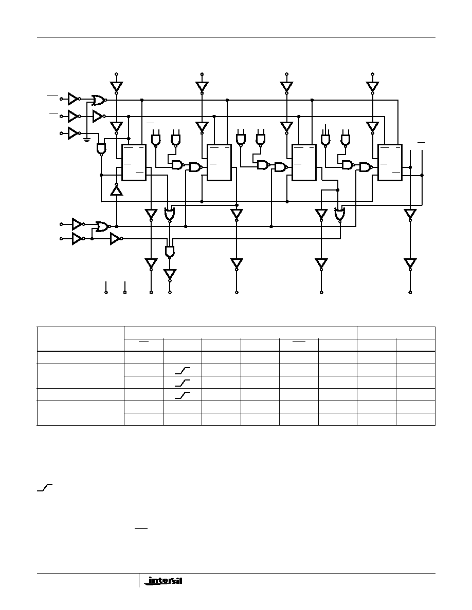
Functional Diagram
TRUTH TABLE
OPERATING MODE
INPUTS
OUTPUTS
MR
CP
PE
TE
SPE
Pn
Qn
TC
Reset (Clear)
L
X
X
X
X
X
L
L
Parallel Load
H
X
X
l
l
L
L
H
X
X
l
h
H
(Note 1)
Count
H
h
h
h (Note 3)
X
Count
(Note 1)
Inhibit
H
X
l (Note 2)
X
h (Note 3)
X
qn
(Note 1)
H
X
X
l (Note 2)
h (Note 3)
X
qn
L
H = HIGH voltage level.
L = LOW voltage level.
h = HIGH voltage level one setup time prior to the LOW-to-HIGH clock transition.
l = LOW voltage level one setup time prior to the LOW-to-HIGH clock transition.
X = Immaterial.
q = Lower case letter indicate the state of the referenced output prior to the LOW-to-HIGH clock transition.
= LOW-to-HIGH clock transition.
NOTES:
1. The TC output is HIGH when TE is HIGH and the counter is at terminal count (HHHH for 161 and HLLH for 160).
2. The HIGH-to-LOW transition of PE or TE on the 54/74161 and 54/74160 should only occur while CP is high for conventional operation.
3. The LOW-to-HIGH transition of SPE on the 54/74161 and 54/74160 should only occur while CP is high for conventional operation.
SPE
MR
CP
PE
TE
MR
D0
T0
CP
P
Q0
Q0
Q0
14
15
TC
MR
D1
T1
CP
P
Q1
Q1
13
MR
D2
T2
CP
P
Q2
Q0
12
MR
D3
T3
CP
P
Q3
Q1
11
Q0
Q3 Q3
Q3 Q0 Q3 Q0
Q0 Q1
Q2 Q3
Q0 Q3
Q0
Q1
Q2
P3
P2
P1
P0
3
4
5
6
GND
V
CC
16
8
HCTS160T
3
All Intersil semiconductor products are manufactured, assembled and tested under ISO9000 quality systems certification.
Intersil semiconductor products are sold by description only. Intersil Corporation reserves the right to make changes in circuit design and/or specifications at any time with-
out notice. Accordingly, the reader is cautioned to verify that data sheets are current before placing orders. Information furnished by Intersil is believed to be accurate and
reliable. However, no responsibility is assumed by Intersil or its subsidiaries for its use; nor for any infringements of patents or other rights of third parties which may result
from its use. No license is granted by implication or otherwise under any patent or patent rights of Intersil or its subsidiaries.
For information regarding Intersil Corporation and its products, see web site http://www.intersil.com
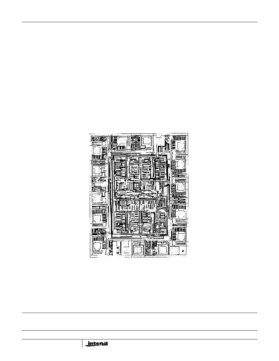
Die Characteristics
DIE DIMENSIONS:
(2642
µ
m x 2184
µ
m x 533
µ
m
±
51.0
µ
m)
104 x 86 x 21mils
±
2mil
METALLIZATION:
Type: Al Si
Thickness: 11.0k
≈
±
1k
≈
SUBSTRATE POTENTIAL:
Unbiased Silicon on Sapphire
BACKSIDE FINISH:
Sapphire
PASSIVATION:
Type: Silox (S
i
O
2
)
Thickness: 13.0k
≈
±
2.6k
≈
WORST CASE CURRENT DENSITY:
< 2.0e5 A/cm
2
TRANSISTOR COUNT:
676
PROCESS:
CMOS SOS
Metallization Mask Layout
HCTS160T
MR
(1)
CD
(2)
P0 (3)
P1 (4)
P2 (5)
P3 (6)
PE (7)
(8)
(9)
SPE
(10)
TE
(11) Q3
(12) Q2
(13) Q1
(14) Q0
(15) TC
V
CC
GND
(16)
NOTE: The die diagram is a generic plot from a similar HCS device. It is intended to indicate approximate die size and bond pad location. The mask
series for the HCTS160 is TA14445A.
HCTS160T