5-142
March 1997
HD-15530
CMOS Manchester Encoder-Decoder
Features
∑ Support of MlL-STD-1553
∑ Data Rate . . . . . . . . . . . . . . . . . . . . . . . . . . . .1.25 MBit/s
∑ Sync Identification and Lock-In
∑ Clock Recovery
∑ Manchester II Encode, Decode
∑ Separate Encode and Decode
∑ Low Operating Power . . . . . . . . . . . . . . . . . 50mW at 5V
Description
The Intersil HD-15530 is a high performance CMOS device
intended to service the requirements of MlL-STD-1553 and
similar Manchester II encoded, time division multiplexed
serial data protocols. This LSI chip is divided into two
sections, an Encoder and a Decoder. These sections
operate completely independent of each other, except for the
Master Reset functions.
This circuit meets many of the requirements of MIL-STD-
1553. The Encoder produces the sync pulse and the parity
bit as well as the encoding of the data bits. The Decoder
recognizes the sync pulse and identifies it as well as decod-
ing the data bits and checking parity.
This integrated circuit is fully guaranteed to support the
1MHz data rate of MlL-STD-1553 over both temperature and
voltage. It interfaces with CMOS, TTL or N channel support
circuitry, and uses a standard 5V supply.
The HD-15530 can also be used in many party line digital
data communications applications, such as an environmen-
tal control system driven from a single twisted pair cable of
fiber optic cable throughout the building.
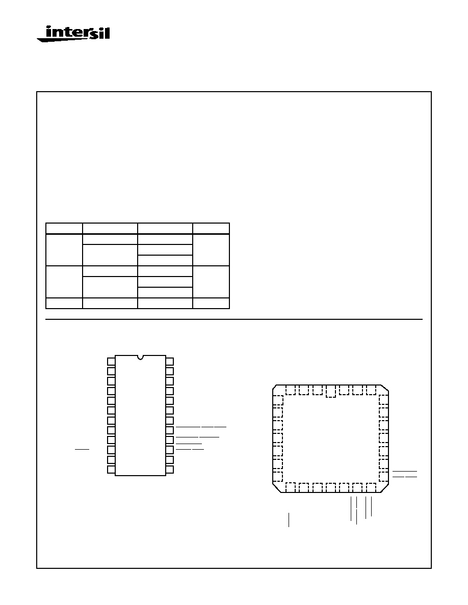
Pinouts
HD-15530 (CERDIP, PDIP)
TOP VIEW
HD-15530 (CLCC)
TOP VIEW
Ordering Information
PACKAGE
TEMP. RANGE
1.25 MEGABIT/s
PKG. NO.
CERDIP
-40
o
C to +85
o
C
HD1-15530-9
F24.6
-55
o
C to +125
o
C
HD1-15530-8
SMD#
7802901JA
CLCC
-40
o
C to +85
o
C
HD4-15530-9
J28.A
-55
o
C to +125
o
C
HD4-15530-8
SMD#
78029013A
PDIP
-40
o
C to +85
o
C
HD3-15530-9
E24.6
1
2
3
4
5
6
7
8
9
10
11
12
16
17
18
19
20
21
22
23
24
15
14
13
VALID WORD
ENCODER
TAKE DATA
SERIAL DATA OUT
DECODER CLK
BIPOLAR ZERO IN
BIPOLAR ONE IN
UNIPOLAR DATA IN
DECODER SHIFT CLK
COMMAND/
DECODER RESET
GND
V
CC
SEND CLK IN
SEND DATA
SYNC SELECT
ENCODER ENABLE
BIPOLAR ONE OUT
BIPOLAR
˜
6 OUT
MASTER RESET
ENCODER CLK
SERIAL DATA IN
OUTPUT INHIBIT
DATA SYNC
SHIFT CLK
ZERO OUT
23
24
25
22
21
20
19
11
3
2
1
4
14
15
16
17
18
12
13
28
27
26
10
5
6
7
8
9
DECODER
NC
NC
BIPOLAR
BIPOLAR
UNIPOLAR
DECODER
SEND
NC
NC
SYNC
ENCODER
SERIAL
BIPOLAR
COMMAND/
DECODER
GND
MASTER
˜
6 OUT
OUTPUT
BIPOLAR
SERIAL
T
AKE D
A
T
A
ENCODER
V
CC
ENCODER
V
ALID
SEND
CLK
ZERO IN
ONE IN
DATA IN
SHIFT CLK
D
A
T
A
OUT
SHIFT CLK
CLK
CLK IN
W
ORD
DATA
SELECT
ENABLE
DATA IN
ONE OUT
D
A
T
A SYNC
RESET
RESET
ZER
O
OUT
INHIBIT
File Number
2960.1
CAUTION: These devices are sensitive to electrostatic discharge; follow proper IC Handling Procedures.
http://www.intersil.com or 407-727-9207
|
Copyright
©
Intersil Corporation 1999
5-143
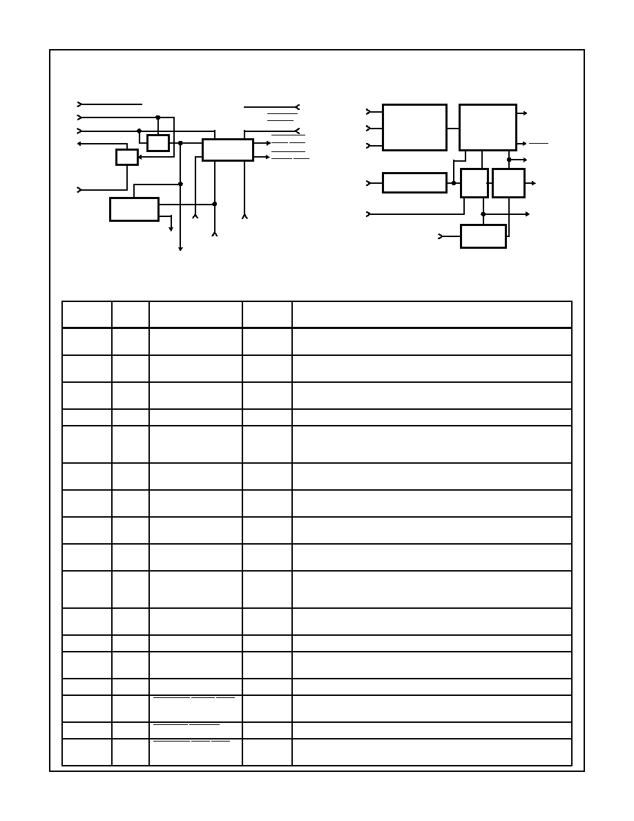
Block Diagrams
ENCODER
DECODER
GND
MASTER RESET
SEND CLK IN
˜
6 OUT
BIT
COUNTER
CHARACTER
12
13
22
14
˜
6
ENCODER
CLK
23
FORMER
˜
2
21
2
18
19
20
15
17
SEND
DATA
SERIAL
DATA IN
ENCODER
ENABLE
SYNC
SELECT
ENCODER
16
BIPOLAR
ONE OUT
BIPOLAR
ZERO OUT
24
OUTPUT
INHIBIT
V
CC
SHIFT CLK
7
6
UNIPOLAR
DATA IN
BIPOLAR
ONE IN
BIPOLAR
ZERO IN
DECODER
CLK
MASTER
RESET
8
TRANSITION
FINDER
SYNCHRONIZER
5
13
DECODER
RESET
11
BIT
COUNTER
BIT
RATE
CLK
PARITY
CHECK
9
1
DECODER
SHIFT
CLK
CHARACTER
IDENTIFIER
10
3
VALID
WORD
SERIAL
DATA OUT
COMMAND/
DATA SYNC
TAKE
DATA
4
Pin Description
PIN
NUMBER
TYPE
NAME
SECTION
DESCRIPTION
1
O
VALID WORD
Decoder
Output high indicates receipt of a valid word, (valid parity and no Manches-
ter errors).
2
O
ENCODER SHIFT
CLOCK
Encoder
Output for shifting data into the Encoder. The Encoder samples SDI on the
low-to-high transition of Encoder Shift Clock.
3
O
TAKE DATA
Decoder
Output is high during receipt of data after identification of a sync pulse and
two valid Manchester data bits.
4
O
SERIAL DATA OUT
Decoder
Delivers received data in correct NRZ format.
5
I
DECODER CLOCK
Decoder
Input drives the transition finder, and the synchronizer which in turn
supplies the clock to the balance of the decoder, input a frequency equal to
12X the data rate.
6
I
BIPOLAR ZERO IN
Decoder
A high input should be applied when the bus is in its negative state. This pin
must be held high when the Unipolar input is used.
7
I
BIPOLAR ONE IN
Decoder
A high input should be applied when the bus is in its positive state. This pin
must be held low when the Unipolar input is used.
8
I
UNLPOLAR DATA IN
Decoder
With pin 6 high and pin 7 low, this pin enters unipolar data into the transition
finder circuit. If not used this input must be held low.
9
O
DECODER SHIFT
CLOCK
Decoder
Output which delivers a frequency (DECODER CLOCK
˜
12), synchro-
nized by the recovered serial data stream.
10
O
COMMAND SYNC
Decoder
Output of a high from this pin occurs during output of decoded data which
was preceded by a Command (or Status) synchronizing character. A low
output indicates a Data synchronizing character.
11
I
DECODER RESET
Decoder
A high input to this pin during a rising edge of DECODER SHIFT CLOCK
resets the decoder bit counting logic to a condition ready for a new word.
12
I
GROUND
Both
Ground Supply pin.
13
I
MASTER RESET
Both
A high on this pin clears 2:1 counters in both Encoder and Decoder, and
resets the
˜
6 circuit.
14
O
˜
6 OUT
Encoder
Output from 6:1 divider which is driven by the ENCODER CLOCK.
15
O
BIPOLAR ZERO OUT
Encoder
An active low output designed to drive the zero or negative sense of a
bipolar line driver.
16
I
OUTPUT INHIBIT
Encoder
A low on this pin forces pin 15 and 17 high, the inactive states.
17
O
BIPOLAR ONE OUT
Encoder
An active low output designed to drive the one or positive sense of a bipolar
line driver.
HD-15530
5-144
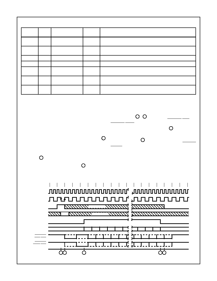
Encoder Operation
The Encoder requires a single clock with a frequency of
twice the desired data rate applied at the SEND CLOCK
input. An auxiliary divide by six counter is provided on chip
which can be utilized to produce the SEND CLOCK by divid-
ing the DECODER CLOCK.
The Encoder's cycle begins when ENCODER ENABLE is
high during a falling edge of ENCODER SHIFT CLOCK
.
This cycle lasts for one word length or twenty ENCODER
SHIFT CLOCK periods. At the next low-to-high transition of
the ENCODER SHIFT CLOCK, a high SYNC SELECT input
actuates a command sync or a low will produce a data sync
for the word
. When the Encoder is ready to accept data,
the SEND DATA output will go high and remain high for six-
teen ENCODER SHIFT CLOCK periods
. During these
sixteen periods the data should be clocked into the SERIAL
DATA input with every high-to-low transition of the
ENCODER SHIFT CLOCK so it can be sampled on the low-
to-high transition
-
. After the sync and Manchester II
coded data are transmitted through the BIPOLAR ONE and
BIPOLAR ZERO outputs, the Encoder adds on an additional
bit which is the parity for that word
. If ENCODER
ENABLE is held high continuously, consecutive words will be
encoded without an interframe gap. ENCODER ENABLE
must go low by time
as shown to prevent a consecutive
word from being encoded. At any time a low on OUTPUT
INHIBIT input will force both bipolar outputs to a high state
but will not affect the Encoder in any other way.
To abort the Encoder transmission a positive pulse must be
applied at MASTER RESET. Anytime after or during this
pulse, a low-to-high transition on SEND CLOCK clears the
internal counters and initializes the Encoder for a new word.
18
I
SERIAL DATA IN
Encoder
Accepts a serial data stream at a data rate equal to ENCODER SHIFT
CLOCK.
19
I
ENCODER ENABLE
Encoder
A high on this pin initiates the encode cycle. (Subject to the preceeding
cycle being complete.)
20
I
SYNC SELECT
Encoder
Actuates a Command sync for an input high and Data sync for an input low.
21
O
SEND DATA
Encoder
An active high output which enables the external source of serial data.
22
I
SEND CLOCK IN
Encoder
Clock input at a frequency equal to the data rate X2, usually driven by
˜
6
output.
23
I
ENCODER CLOCK
Encoder
Input to the 6:1 divider, a frequency equal to the data rate X12 is usually
input here.
24
I
V
CC
Both
V
CC
is the +5V power supply pin. A 0.1
µ
F decoupling capacitor from V
CC
(pin 24) to GROUND (pin 12) is recommended.
I = Input
O = Output
Pin Description
(Continued)
PIN
NUMBER
TYPE
NAME
SECTION
DESCRIPTION
1
2
3
3
4
5
5
FIGURE 1.
DON'T CARE
VALID
DON'T CARE
P
0
1
2
3
P
0
1
2
3
0
1
2
3
19
15
16
17
18
7
6
5
4
11
12
13
14
15
11
12
13
14
15
11
12
13
14
15
10
SYNC
SYNC
2ND HALF
1ST HALF
3
2
1
0
TIMING
SEND CLK
ENCODER
SHIFT CLK
ENCODER
SYNC SELECT
SEND DATA
SERIAL
BIPOLAR
ONE OUT
BIPOLAR
ZERO OUT
1
2
3
4
5
ENABLE
DATA IN
HD-15530
5-145
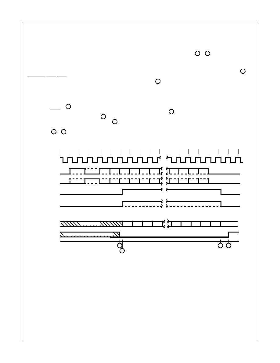
Decoder Operation
The Decoder requires a single clock with a frequency of 12
times the desired data rate applied at the DECODER
CLOCK input. The Manchester II coded data can be
presented to the Decoder in one of two ways. The BIPOLAR
ONE and BIPOLAR ZERO inputs will accept data from a
comparator sensed transformer coupled bus as specified in
Military Spec 1553. The UNIPOLAR DATA input can only
accept non-inverted Manchester II coded data. (e.g. from
BIPOLAR ONE OUT of an Encoder through an inverter to
Unipolar Data Input).
The Decoder is free running and continuously monitors its
data input lines for a valid sync character and two valid
Manchester data bits to start an output cycle. When a valid
sync is recognized
, the type of sync is indicated on
COMMAND/DATA SYNC output. If the sync character was a
command sync, this output will go high
and remain high
for sixteen DECODER SHIFT CLOCK periods
, otherwise
it will remain low. The TAKE DATA output will go high and
remain high
-
while the Decoder is transmitting the
decoded data through SERIAL DATA OUT. The decoded
data available at SERIAL DATA OUT is in NRZ format. The
DECODER SHIFT CLOCK is provided so that the decoded
bits can be shifted into an external register on every low-to-
high transition of this clock
-
. Note that DECODER
SHIFT CLOCK may adjust its phase up until the time that
TAKE DATA goes high.
After all sixteen decoded bits have been transmitted
the
data is checked for odd parity. A high on VALID WORD
output
indicates a successful reception of a word without
any Manchester or parity errors. At this time the Decoder is
looking for a new sync character to start another output
sequence. VALID WORD will go low approximately 20
DECODER SHIFT CLOCK periods after it goes high if not
reset low sooner by a valid sync and two valid Manchester
bits as shown
.
At any time in the above sequence a high input on
DECODER RESET during a low-to-high transition of
DECODER SHIFT CLOCK will abort transmission and ini-
tialize the Decoder to start looking for a new sync character.
1
2
3
2
3
2
3
3
4
1
FIGURE 2.
UNDEFINED
P
0
1
2
P
0
1
2
1
2
3
4
0
16
17
18
19
7
6
5
4
11
12
13
14
15
11
12
13
14
15
12
13
14
15
SYNC
SYNC
2ND HALF
1ST HALF
3
2
1
0
TIMING
DECODER
SHIFT CLK
COMMAND/
TAKE DATA
SERIAL
8
10
10
1
2
3
4
DATA OUT
BIPOLAR
ONE IN
BIPOLAR
ZERO IN
(FROM PREVIOUS RECEPTION)
VALID WORD
DATA SYNC
HD-15530
5-146
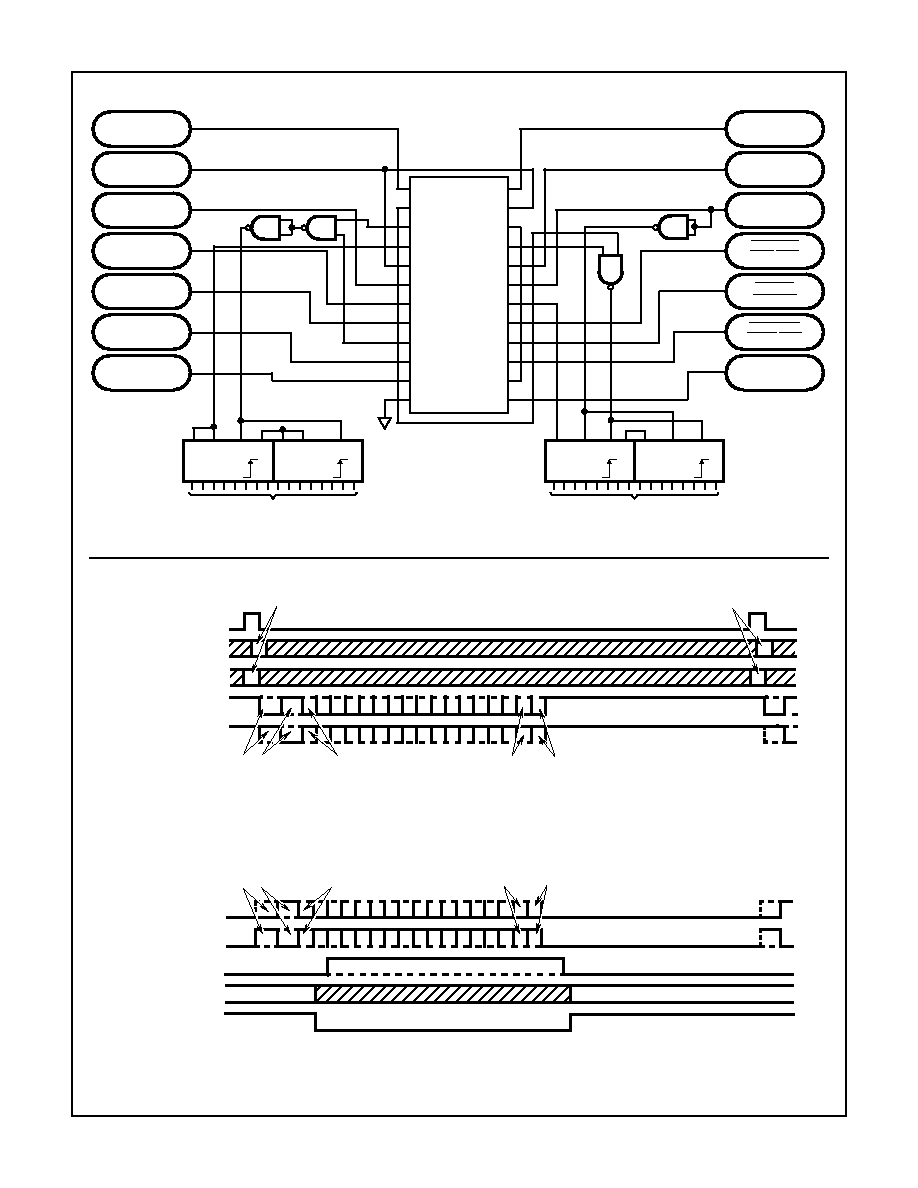
How to Make Our MTU Look Like a Manchester Encoded UART
Typical Timing Diagrams for a Manchester Encoded UART
FIGURE 4. ENCODER TIMING
FIGURE 5. DECODER TIMING
FIGURE 3.
1
2
3
4
5
6
7
8
9
10
11
12
16
17
18
19
20
21
22
23
24
15
14
13
VALID WORD
DECODER
BIPOLAR
BIPOLAR
UNIPOLAR
COMMAND
DECODER
V
CC
SYNC
ENCODER
BIPOLAR
BIPOLAR
MASTER
OUTPUT
SYNC
ENCODER CLK
ZERO OUT
RESET
DATA IN
ONE IN
ZERO IN
SELECT
ENABLE
ONE OUT
INHIBIT
RESET
A
B
CK H
74LS164
A
B
CK
74LS164
PARALLEL OUT
O
H
SH/LD CK SI
74165
CK
74165
PARALLEL IN
SH/LD
O
H
ENCODER ENABLE
SYNC SELECT
PARALLEL IN
VALID
VALID
BIPOLAR ONE OUT
BIPOLAR ZERO OUT
SYNC
MSB
LSB
PARITY
P
P
SYNC
MSB
LSB
PARITY
P
BIPOLAR ONE IN
BIPOLAR ZERO IN
COMMAND SYNC
PARALLEL OUT
VALID WORD
FROM
PREVIOUS
RECEPTION
VALID
VALID
P
HD-15530

5-147
MIL-STD-1553
The 1553 standard defines a time division multiplexed data
bus for application within aircraft. The bus is defined to be
bipolar, and encoded in a Manchester II format, so no DC
component appears on the bus. This allows transformer
coupling and excellent isolation among systems and their
environment.
The HD-15530 supports the full bipolar configuration,
assuming a bus driver configuration similar to that in Figure
1. Bipolar inputs from the bus, like Figure 2, are also accom-
modated.
The signaling format in MlL-STD-1553 is specified on the
assumption that the network of 32 or fewer terminals are
controlled by a central control unit by means of Command
Words. Terminals respond with Status Words. Each word is
preceded by a synchronizing pulse, and followed by parity
bit, occupying a total of 20
µ
s. The word formats are shown in
Figure 4. The special abbreviations are as follows:
P
Parity, which is defined to be odd, taken across all 17
bits.
R/T
Receive on logical zero, transmit on ONE.
ME
Message Error if logical 1.
TF
Terminal Flat, if set, calls for controller to request
self-test data.
The paragraphs above are intended only to suggest the
content of MlL-STD-1553, and do not completely describe its
bus requirements, timing or protocols.
FIGURE 6. SIMPLIFIED MIL-STD-1553 DRIVER
FIGURE 7. SIMPLIFIED MIL-STD-1553 RECEIVER
FIGURE 8. MIL-STD-1553 CHARACTER FORMATS
FIGURE 9. MIL-STD-1553 WORD FORMATS
NOTE: This page is a summary of MIL-STD-1553 and is not intended to describe the operation of the HD-15530.
"1"
"0"
BUS
"0"
"1"
BUS
+
-
+
-
"1" REF
"0" REF
COMMAND
SYNC
SYNC
DATA
PERIOD
BIT
PERIOD
BIT
PERIOD
BIT
LOGICAL ONE DATA
LOGICAL ZERO DATA
19
18
17
16
15
14
13
12
11
10
9
8
7
6
5
4
3
2
1
0
5
5
5
1
P
DATA WORD
COUNT
SUB ADDRESS
/MODE
TERMINAL
ADDRESS
SYNC
COMMAND WORD (FROM CONTROLLER TO TERMINAL)
1
R/T
16
1
P
SYNC
DATA WORD (SENT EITHER DIRECTION)
5
9
1
P
CODE FOR FAILURE MODES
TERMINAL
ADDRESS
SYNC
STATUS WORD (FROM TERMINAL TO CONTROLLER)
1
ME
TF
1
CONTROL WORD
HD-15530
5-148
Absolute Maximum Ratings
Thermal Information
Supply Voltage . . . . . . . . . . . . . . . . . . . . . . . . . . . . . . . . . . . . . +7.0V
Input, Output or I/O Voltage . . . . . . . . . . . . GND-0.3V to V
CC
+0.3V
ESD Classification . . . . . . . . . . . . . . . . . . . . . . . . . . . . . . . . Class 1
Operating Conditions
Supply Voltage . . . . . . . . . . . . . . . . . . . . . . . . . . . . . +4.5V to +5.5V
Temperature Range (T
A
)
HD-15530-9 . . . . . . . . . . . . . . . . . . . . . . . . . . . . . -40
o
C to +85
o
C
HD-15530-8 . . . . . . . . . . . . . . . . . . . . . . . . . . . . -55
o
C to +125
o
C
Encoder/Decoder Clock Rise Time . . . . . . . . . . . . . . . . . . .8ns Max
Encoder/Decoder Clock Fall Time . . . . . . . . . . . . . . . . . . . .8ns Max
Sync Transition Span (TD2) . . . . . . . . . . . . . . . 18 TDC Typ (Note 1)
Short Data Transition Span (TD4) . . . . . . . . . . . 6 TDC Typ (Note 1)
Long Data Transition Span (TD5) . . . . . . . . . . . 12 TDC Typ (Note 1)
Thermal Resistance (Typical)
JA
(
o
C/W)
JC
(
o
C/W)
CERDIP Package . . . . . . . . . . . . . . . .
55
12
CLCC Package . . . . . . . . . . . . . . . . . .
65
14
Plastic DIP Package . . . . . . . . . . . . . .
60
N/A
Maximum Junction Temperature
Ceramic Package . . . . . . . . . . . . . . . . . . . . . . . . . . . . . . . +175
o
C
Plastic Package . . . . . . . . . . . . . . . . . . . . . . . . . . . . . . . . . . 150
o
C
Maximum Storage Temperature Range . . . . . . . . .-65
o
C to +150
o
C
Maximum Lead Temperature (Soldering 10s) . . . . . . . . . . . . +300
o
C
Die Characteristics
Gate Count . . . . . . . . . . . . . . . . . . . . . . . . . . . . . . . . . . . . 456 Gates
CAUTION: Stresses above those listed in "Absolute Maximum Ratings" may cause permanent damage to the device. This is a stress only rating and operation of
the device at these or any other conditions above those indicated in the operational sections of this specification is not implied.
DC Electrical Specifications
V
CC
= 5V
±
10%, T
A
= -40
o
C to +85
o
C (HD-15530-9)
T
A
= -55
o
C to +125
o
C (HD-15530-8)
PARAMETER
SYMBOL
LIMITS
TEST CONDITIONS
UNITS
MIN
MAX
Input LOW Voltage
V
IL
-
0.2 V
CC
V
CC
= 4.5V and 5.5V
V
Input HIGH Voltage
V
lH
0.7 V
CC
-
V
CC
= 4.5V and 5.5V
V
Input LOW Clock Voltage
V
ILC
-
GND +0.5
V
CC
= 4.5V and 5.5V
V
Input HIGH Clock Voltage
V
IHC
V
CC
-0.5
-
V
CC
= 4.5V and 5.5V
V
Output LOW Voltage
V
OL
-
0.4
I
OL
= 1.8mA (Note 2), V
CC
= 4.5V
V
Output HIGH Voltage
V
OH
2.4
-
I
OH
= -3mA (Note 2), V
CC
= 4.5V
V
Input Leakage Current
I
I
-1.0
+1.0
V
I
= GND or V
CC
, V
CC
= 5.5V
µ
A
Standby Supply Current
I
CCSB
-
2
V
IN
= V
CC
= 5.5V Output Open
mA
Operating Power Supply Current
I
CCOP
-
10
V
CC
= 5.5V, V
IN
= V
CC
, f =15MHz, Outputs Open
mA
Function Test
F
T
-
-
(Note 3)
-
NOTES:
1. TDC = Decoder clock period = 1/FDC
2. Interchanging of force and sense conditions is permitted.
3. Tested as follows: = f = 15MHz, V
IH
= 70% V
CC
, V
IL
= 20% V
CC
, C
L
= 50pF, V
OH
1.5V and V
OL
1.5V.
Capacitance
T
A
= +25
o
C; Frequency = 1MHz
SYMBOL
PARAMETER
TYPICAL
UNITS
CONDITIONS
C
IN
Input Capacitance
15
pF
All measurements are referenced to device GND
C
O
Output Capacitance
15
pF
HD-15530
5-149
AC Electrical Specifications
V
CC
= 5V
±
10%, T
A
= -40
o
C to +85
o
C (HD-15530-9)
T
A
= -55
o
C to +125
o
C (HD-15530-8)
PARAMETER
SYMBOL
(NOTE 2)
TEST CONDITIONS
LIMITS
UNITS
MIN
MAX
ENCODER TIMING
Encoder Clock Frequency
FEC
V
CC
= 4.5V and 5.5V, C
L
= 50pF
-
15
MHz
Send Clock Frequency
FESC
V
CC
= 4.5V and 5.5V, C
L
= 50pF
-
2.5
MHz
Encoder Data Rate
FED
V
CC
= 4.5V and 5.5V, C
L
= 50pF
-
1.25
MHz
Master Reset Pulse Width
TMR
V
CC
= 4.5V and 5.5V, C
L
= 50pF
150
-
ns
Shift Clock Delay
TE1
V
CC
= 4.5V and 5.5V, C
L
= 50pF
-
125
ns
Serial Data Setup
TE2
V
CC
= 4.5V and 5.5V, C
L
= 50pF
75
-
ns
Serial Data Hold
TE3
V
CC
= 4.5V and 5.5V, C
L
= 50pF
75
-
ns
Enable Setup
TE4
V
CC
= 4.5V and 5.5V, C
L
= 50pF
90
-
ns
Enable Pulse Width
TE5
V
CC
= 4.5V and 5.5V, C
L
= 50pF
100
-
ns
Sync Setup
TE6
V
CC
= 4.5V and 5.5V, C
L
= 50pF
55
-
ns
Sync Pulse Width
TE7
V
CC
= 4.5V and 5.5V, C
L
= 50pF
150
-
ns
Send Data Delay
TE8
V
CC
= 4.5V and 5.5V, C
L
= 50pF
0
50
ns
Bipolar Output Delay
TE9
V
CC
= 4.5V and 5.5V, C
L
= 50pF
-
130
ns
Enable Hold
TE10
V
CC
= 4.5V and 5.5V, C
L
= 50pF
10
-
ns
Sync Hold
TE11
V
CC
= 4.5V and 5.5V, C
L
= 50pF
95
-
ns
DECODER TIMING
Decoder Clock Frequency
FDC
V
CC
= 4.5V and 5.5V, C
L
= 50pF
-
15
MHz
Decoder Data Rate
FDD
V
CC
= 4.5V and 5.5V, C
L
= 50pF
-
1.25
MHz
Decoder Reset Pulse Width
TDR
V
CC
= 4.5V and 5.5V, C
L
= 50pF
150
-
ns
Decoder Reset Setup Time
TDRS
V
CC
= 4.5V and 5.5V, C
L
= 50pF
75
-
ns
Decoder Reset Hold Time
TDRH
V
CC
= 4.5V and 5.5V, C
L
= 50pF
10
-
ns
Master Reset Pulse
TMR
V
CC
= 4.5V and 5.5V, C
L
= 50pF
150
-
ns
Bipolar Data Pulse Width
TD1
V
CC
= 4.5V and 5.5V, C
L
= 50pF
TDC + 10
(Note 1)
-
ns
One Zero Overlap
TD3
V
CC
= 4.5V and 5.5V, C
L
= 50pF
-
TDC - 10
(Note 1)
ns
Sync Delay (ON)
TD6
V
CC
= 4.5V and 5.5V, C
L
= 50pF
-20
110
ns
Take Data Delay (ON)
TD7
V
CC
= 4.5V and 5.5V, C
L
= 50pF
0
110
ns
Serial Data Out Delay
TD8
V
CC
= 4.5V and 5.5V, C
L
= 50pF
-
80
ns
Sync Delay (OFF)
TD9
V
CC
= 4.5V and 5.5V, C
L
= 50pF
0
110
ns
Take Data Delay (OFF)
TD10
V
CC
= 4.5V and 5.5V, C
L
= 50pF
0
110
ns
Valid Word Delay
TD11
V
CC
= 4.5V and 5.5V, C
L
= 50pF
0
110
ns
NOTES:
1. TDC = Decoder clock period = 1/FDC
2. AC Testing as follows: Input levels: V
IH
= 70% V
CC
, V
IL
= 20% V
CC
; Input rise/fall times driven at 1ns/V; Timing Reference levels: 1.5V;
Output load: C
L
= 50pF.
HD-15530
5-150
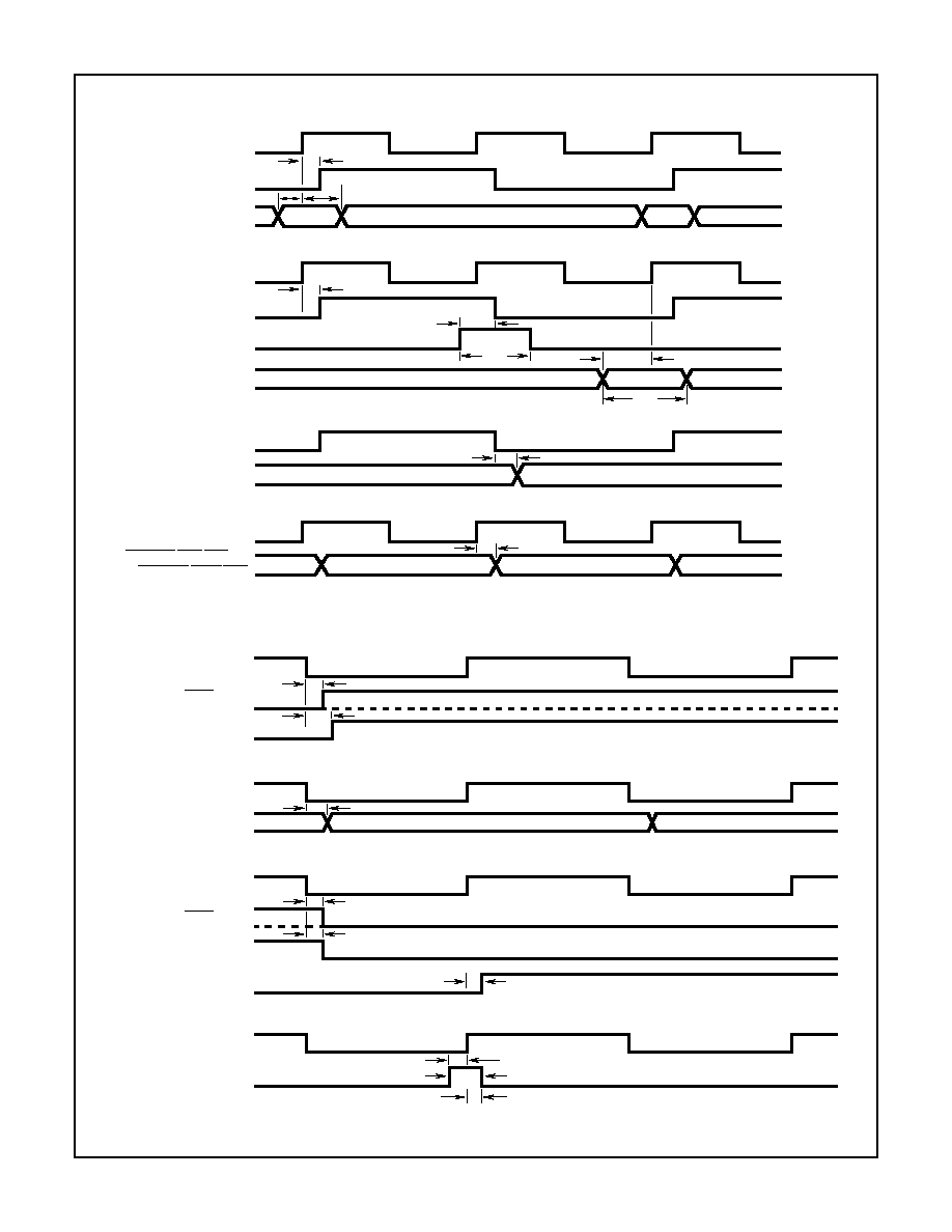
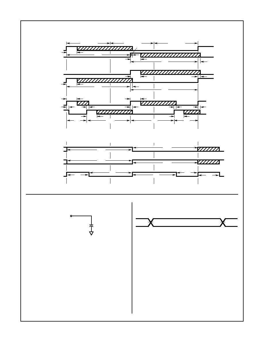
Timing Waveforms
FIGURE 10. ENCODER TIMING
FIGURE 11. DECODER TIMING
SEND CLOCK
ENCODER SHIFT CLOCK
SERIAL DATA IN
SEND CLOCK
ENCODER SHIFT CLOCK
ENCODER ENABLE
SYNC SELECT
ENCODER SHIFT CLOCK
SEND DATA
SEND CLOCK
BIPOLAR ONE OUT OR
BIPOLAR ZERO OUT
T
E9
T
E8
T
E7
VALID
T
E6
T
E5
T
E4
T
E1
T
E3
T
E2
VALID
VALID
T
E1
DECODER SHIFT CLOCK
COMMAND/DATA SYNC
TAKE DATA
DECODER SHIFT CLOCK
SERIAL DATA OUT
DECODER SHIFT CLOCK
COMMAND/DATA SYNC
TAKE DATA
VALID WORD
DECODER SHIFT CLOCK
DECODER RESET
T
D6
T
D7
T
D8
T
D9
T
D10
T
D11
T
DRS
T
DR
T
DRH
DATA BIT
HD-15530
5-151
Test Load Circuit
AC Testing Input, Output Waveform
FIGURE 12. DECODER TIMING
Timing Waveforms
(Continued)
BIPOLAR ONE IN
T
D1
BIPOLAR ZERO IN
BIPOLAR ONE IN
BIPOLAR ZERO IN
BIPOLAR ONE IN
BIPOLAR ZERO IN
UNIPOLAR IN
T
D2
T
D3
T
D1
T
D2
T
D3
BIT PERIOD
BIT PERIOD
BIT PERIOD
COMMAND SYNC
T
D1
T
D2
T
D3
T
D1
DATA SYNC
T
D2
T
D3
T
D1
T
D3
T
D3
T
D1
T
D1
T
D1
T
D3
T
D3
T
D3
T
D4
T
D5
T
D5
T
D4
ONE
ZERO
ONE
T
D2
COMMAND SYNC
T
D2
T
D2
T
D2
T
D5
T
D5
T
D4
T
D4
T
D4
UNIPOLAR IN
UNIPOLAR IN
ONE
ZERO
ONE
DATA SYNC
ONE
NOTE: BIPOLAR ONE IN = 0; BIPOLAR ZERO IN = 1, FOR NEXT DIAGRAMS.
NOTE: UNIPOLAR IN = 0, FOR NEXT DIAGRAMS.
CL9
DUT
NOTE: Includes stray and jig capacitance.
(NOTE)
INPUT
V
IH
V
IL
50%
50%
V
OH
V
OL
OUTPUT
AC Testing: All input signals must switch between V
IL
and V
IH
. Input
rise and fall times are driven at 1ns per volt.
HD-15530

5-152
Burn-In Circuits
HD1-15530 CERDIP
HD4-15530 CLCC
NOTES:
1. V
CC
= 5.5V
±
0.5V
2. V
IH
= 4.5V
±
10%
3. V
IL
= -0.2V +0.4V
4. R1 = 47K
±
5%
5. R2 = 1.8K
±
5%
6. F0 = 100KHz
±
10%
7. C1 = 0.01
µ
F Min.
1
2
3
4
5
6
7
8
9
10
11
12
16
17
18
19
20
21
22
23
24
15
14
13
R1
GND
V
CC
R1
A
R1
GND
R1
R1
A
A
GND
F0
A
A
A
A
R1
R1
R1
R1
GND
V
CC
R1
GND
R1
V
CC
R1
GND
R1
F0
A
GND
V
CC
GND
V
CC
C1
23
24
25
22
21
20
19
11
3
2
1
4
14
15
16
17
18
12
13
28
27
26
10
5
6
7
8
9
GND
V
CC
R2
R2
GND
V
CC
GND
R2
R2
F0
GND
R2
R2
V
CC
R2
GND
R2
GND
GND
C1
GND
GND
NC
NC
R2
GND
GND
GND
GND
NC
NC
F0
HD-15530
5-153
All Intersil semiconductor products are manufactured, assembled and tested under ISO9000 quality systems certification.
Intersil products are sold by description only. Intersil Corporation reserves the right to make changes in circuit design and/or specifications at any time without
notice. Accordingly, the reader is cautioned to verify that data sheets are current before placing orders. Information furnished by Intersil is believed to be accurate
and reliable. However, no responsibility is assumed by Intersil or its subsidiaries for its use; nor for any infringements of patents or other rights of third parties which
may result from its use. No license is granted by implication or otherwise under any patent or patent rights of Intersil or its subsidiaries.
For information regarding Intersil Corporation and its products, see web site http://www.intersil.com
Die Characteristics
DIE DIMENSIONS:
155 x 195 x 19mils
METALLIZATION:
Type: Si-Al
Thickness: 11k
≈
±
2k
≈
GLASSIVATION:
Type: SiO
2
Thickness: 8kA
±
1k
≈
WORST CASE CURRENT DENSITY:
1.8 x 10
5
A/cm
2
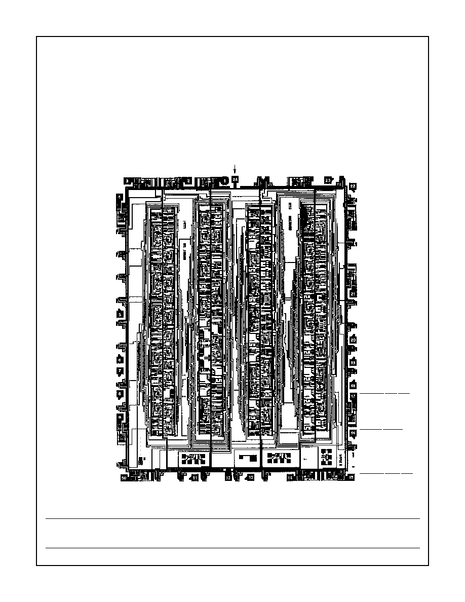
Metallization Mask Layout
HD-15530
ENCODER
VALID
ENCODER CLK
SEND CLK IN
SEND DATA
SYNC SELECT
ENCODER ENABLE
COMMAND/DATA SYNC
DECODER SHIFT CLK
UNIPOLAR DATA IN
BIPOLAR ONE IN
˜
6 OUT
MASTER
GND
WORD
SHIFT CLK
SERIAL DATA IN
BIPOLAR ONE OUT
OUTPUT INHIBIT
BIPOLAR ZERO OUT
RESET
DECODER
RESET
BIPOLAR ZERO IN
DECODER CLK
SERIAL DATA OUT
TAKE DATA
V
CC
HD-15530