107
TM
March 1997
HD-6402/883
CMOS Universal Asynchronous
Receiver Transmitter (UART)
Features
∑ This Circuit is Processed in Accordance to MIL-STD-
883 and is Fully Conformant Under the Provisions of
Paragraph 1.2.1.
∑ 8.0MHz Operating Frequency (HD-6402/883B)
∑ 2.0MHz Operating Frequency (HD-6402/883R)
∑ Low Power CMOS Design
∑ Programmable Word Length, Stop Bits and Parity
∑ Automatic Data Formatting and Status Generation
∑ Compatible with Industry Standard UARTs
∑ Single +5V Power Supply
∑ CMOS/TTL Compatible Inputs
Description
The HD-6402/883 is a CMOS UART for interfacing comput-
ers or microprocessors to an asynchronous serial data chan-
nel. The receiver converts serial start, data, parity and stop
bits. The transmitter converts parallel data into serial form
and automatically adds start, parity and stop bits. The data
word length can be 5, 6, 7 or 8 bits. Parity may be odd or
even. Parity checking and generation can be inhibited. The
stop bits may be one or two or one and one-half when trans-
mitting 5-bit code.
The HD-6402/883 can be used in a wide range of applica-
tions including modems, printers, peripherals and remote
data acquisition systems. Utilizing the Intersil advanced
scaled SAJI IV CMOS process permits operation clock fre-
quencies up to 8.0MHz (500K Baud). Power requirements,
by comparison, are reduced from 300mW to 10mW. Status
logic increases flexibility and simplifies the user interface.
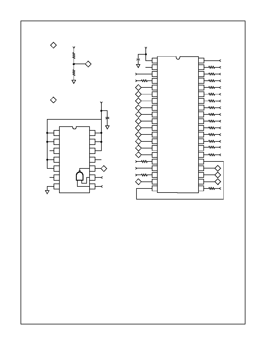
Pinout
HD-6402/883 (CERDIP)
TOP VIEW
Ordering Information
PACKAGE
TEMPERATURE RANGE
2MHz = 125K BAUD
8MHz = 500K BAUD
PKG. NO.
CERDIP
-55
o
C to +125
o
C
HD1-6402R/883
HD1-6402B/883
F40.6
13
1
2
3
4
5
6
7
8
9
10
11
12
14
15
16
17
18
19
20
VCC
NC
GND
RRD
RBR8
RBR7
RBR6
RBR5
RBR4
RBR3
RBR2
RBR1
PE
FE
OE
SFD
RRC
DRR
DR
RRI
28
40
39
38
37
36
35
34
33
32
31
30
29
27
26
25
24
23
22
21
TRC
EPE
CLS1
CLS2
SBS
PI
CRL
TBR8
TBR7
TBR6
TBR5
TBR4
TBR3
TBR2
TBR1
TRO
TRE
TBRL
TBRE
MR
FN2953.1
CAUTION: These devices are sensitive to electrostatic discharge; follow proper IC Handling Procedures.
1-888-INTERSIL or 321-724-7143
|
Intersil (and design) is a trademark of Intersil Americas Inc.
Copyright © Intersil Americas Inc. 2002. All Rights Reserved
109
Absolute Maximum Ratings
Thermal Information
Supply Voltage . . . . . . . . . . . . . . . . . . . . . . . . . . . . . . . . . . . . . +8.0V
Input, Output or I/O Voltage Applied. . . . . GND -0.5V to V
CC
+0.5V
Storage Temperature Range . . . . . . . . . . . . . . . . . -65
o
C to +150
o
C
Junction Temperature. . . . . . . . . . . . . . . . . . . . . . . . . . . . . . +175
o
C
Lead Temperature (Soldering 10s). . . . . . . . . . . . . . . . . . . . +300
o
C
ESD Classification . . . . . . . . . . . . . . . . . . . . . . . . . . . . . . . . Class 1
Typical Derating Factor . . . . . . . . . . . 1mA/MHz Increase in ICCOP
Thermal Resistance
JA
JC
CERDIP Package . . . . . . . . . . . . . . . .
50
o
C/W
12
o
C/W
Gate Count . . . . . . . . . . . . . . . . . . . . . . . . . . . . . . . . . . . 1643 Gates
CAUTION: Stresses above those listed in "Absolute Maximum Ratings" may cause permanent damage to the device. This is a stress only rating and operation
of the device at these or any other conditions above those indicated in the operational sections of this specification is not implied.
Operating Conditions
Operating Voltage Range . . . . . . . . . . . . . . . . . . . . . +4.5V to +5.5V
Operating Temperature Range . . . . . . . . . . . . . . . .-55
o
C to +125
o
C
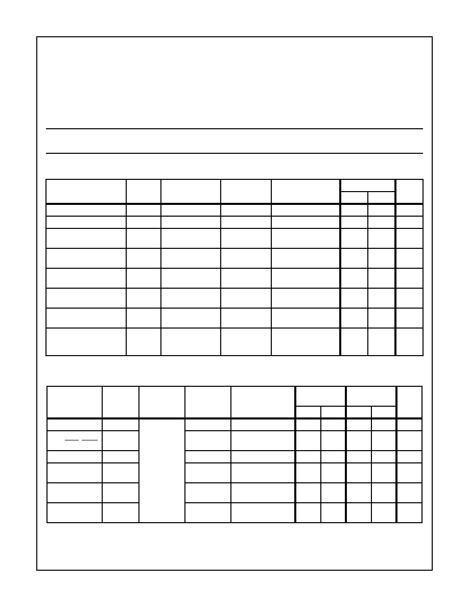
TABLE 1. HD-6402/883 D.C. ELECTRICAL PERFORMANCE SPECIFICATIONS
Device Guaranteed and 100% Tested
D.C. PARAMETER
SYMBOL
CONDITIONS
GROUP A
SUBGROUPS
TEMPERATURE
LIMITS
UNITS
MIN
MAX
Logical ``1'' Input Voltage
VIH
VCC = 5.5V
1, 2, 3
-55
o
C
T
A
+125
o
C
2.3
-
V
Logical ``0'' Input Voltage
VIL
VCC = 4.5V
1, 2, 3
-55
o
C
T
A
+125
o
C
-
0.8
V
Input Leakage Current
IID
VIN = GND or VCC,
VCC = 5.5V
1, 2, 3
-55
o
C
T
A
+125
o
C
-1.0
1.0
µ
A
Logical ``1'' Output Voltage
VOH
IOH = -2.5mA,
VCC = 4.5V (Note 1)
1, 2, 3
-55
o
C
T
A
+125
o
C
3.0
-
V
Logical ``1'' Output Voltage
VOH
IOH = -100
µ
A
VCC = 4.5V (Note 1)
1, 2, 3
-55
o
C
T
A
+125
o
C
VCC
-0.4
-
V
Logical ``0'' Output Voltage
VOL
IOL = +2.5mA,
VCC = 4.5V (Note 1)
1, 2, 3
-55
o
C
T
A
+125
o
C
-
0.4
V
Output Leakage Current
IO
VO = GND or VCC,
VCC = 5.5V
1, 2, 3
-55
o
C
T
A
+125
o
C
-1.0
1.0
µ
A
Standby Supply Current
ICCSB
VIN = GND or VCC;
VCC = 5.5V,
Output Open
1, 2, 3
-55
o
C
T
A
+125
o
C
-
100
µ
A
TABLE 2. HD-6402/883 A.C. ELECTRICAL PERFORMANCE SPECIFICATIONS
Device Guaranteed and 100% Tested
A.C.
PARAMETER
SYMBOL
(NOTE 1)
CONDITIONS
GROUP A
SUBGROUPS
TEMPERATURE
LIMITS
HD-6402/883R
LIMITS
HD-6402/883B
UNITS
MIN
MAX
MIN
MAX
Clock Frequency
(1) fCLOCK
VCC = 4.5V
CL = 50pF
9, 10, 11
-55
o
C
T
A
+125
o
C
-
2.0
-
8.0
MHz
Pulse Widths,
CRL, DRR, TBRL
(2) tPW
9, 10, 11
-55
o
C
T
A
+125
o
C
150
-
75
-
ns
Pulse Width MR
(3) tMR
9, 10, 11
-55
o
C
T
A
+125
o
C
150
-
150
-
ns
Input Data Setup
Time
(4) tSET
9, 10, 11
-55
o
C
T
A
+125
o
C
50
-
20
-
ns
Input Data Hold
Time
(5) tHOLD
9, 10, 11
-55
o
C
T
A
+125
o
C
60
-
20
-
ns
Output Enable
Time
(6) tEN
9, 10, 11
-55
o
C
T
A
+125
o
C
-
160
-
35
ns
NOTE:
1. Interchanging of force and sense conditions is permitted.
2. Tested with input levels of VIH = 2.76V and VIL = 0.4V. Rise and fall times are driven at 1ns/V.
HD-6402/883
110
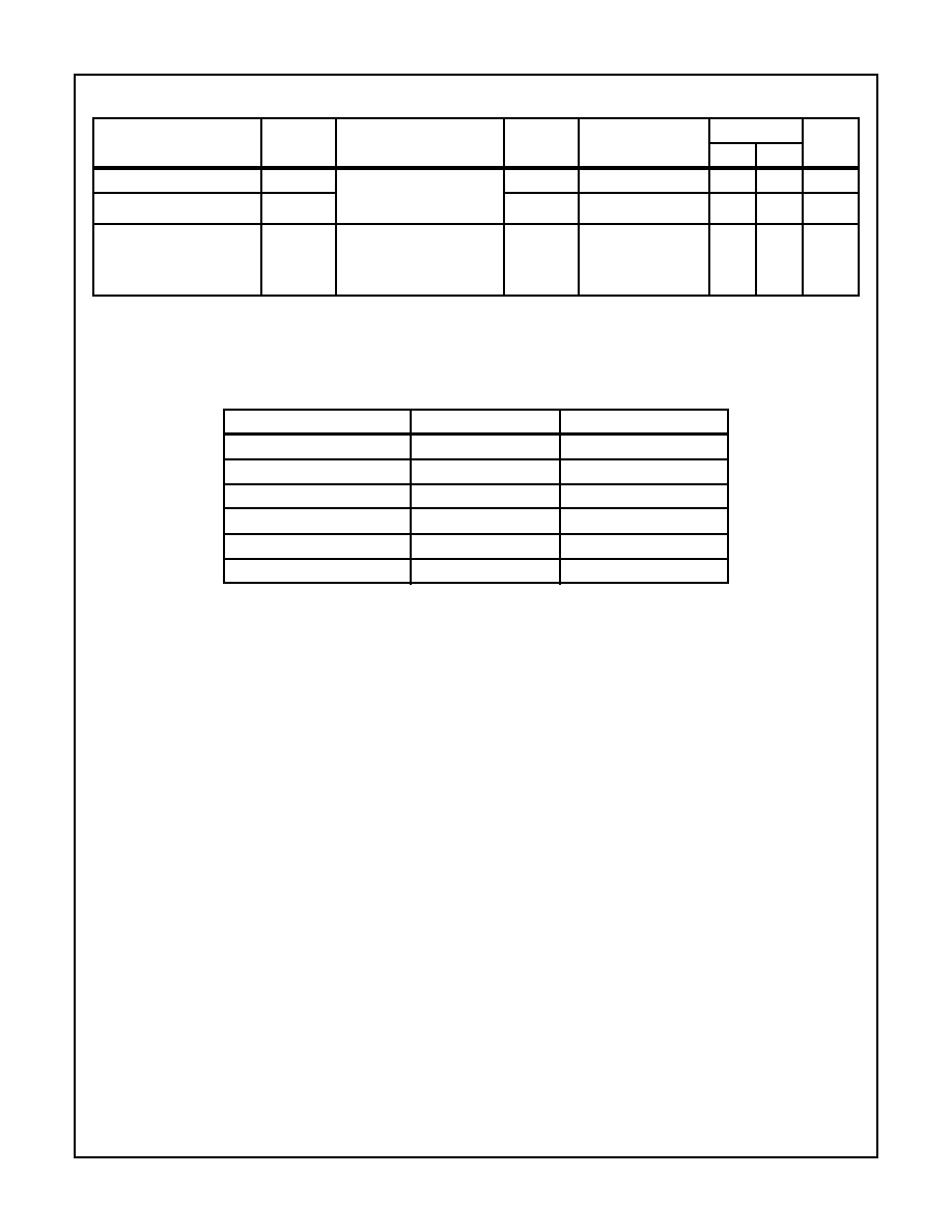
TABLE 3. HD-6402/883 ELECTRICAL PERFORMANCE SPECIFICATIONS
A.C. PARAMETER
SYMBOL
CONDITIONS
NOTES
TEMPERATURE
LIMITS
UNITS
MIN
MAX
Input Capacitance
CIN
f = 1Mhz
All Measurements are
Referenced to Device GND
1
T
A
= +25
o
C
-
25.0
pF
Output Capacitance
CO
1
T
A
= +25
o
C
-
25.0
pF
Operating Supply Current
ICCOP
VCC = 5.5V,
Clock Freq. = 2MHz,
VIN = VCC or GND,
Outputs Open
1
-55
o
C
T
A
+125
o
C
-
2.0
mA
NOTE:
1. The parameters listed in Table 3 are controlled via design or process parameters and are not directly tested. These parameters are char-
acterized upon initial design and after major process and/or design changes.
TABLE 4. APPLICABLE SUBGROUPS
CONFORMANCE GROUPS
METHOD
SUBGROUPS
Initial Test
100%/5004
-
Interim Test
100%/5004
1, 7, 9
PDA
100%
1
Final Test
100%
2, 3, 8A, 8B, 10, 11
Group A
-
1, 2, 3, 7, 8A, 8B, 9, 10, 11
Group C and D
Samples/5005
1, 7, 9
HD-6402/883