135
TM
March 1997
HD-6409/883
CMOS Manchester Encoder-Decoder
Features
∑ This Circuit is Processed in Accordance to MIL-STD-
883 and is Fully Conformant Under the Provisions of
Paragraph 1.2.1.
∑ Converter or Repeater Mode
∑ Independent Manchester Encoder and Decoder
Operation
∑ Static to One Megabit/Sec Data Rate Guaranteed
∑ Low Bit Error Rate
∑ Digital PLL Clock Recovery
∑ On Chip Oscillator
∑ Low Operating Power: 50mW Typical at +5V
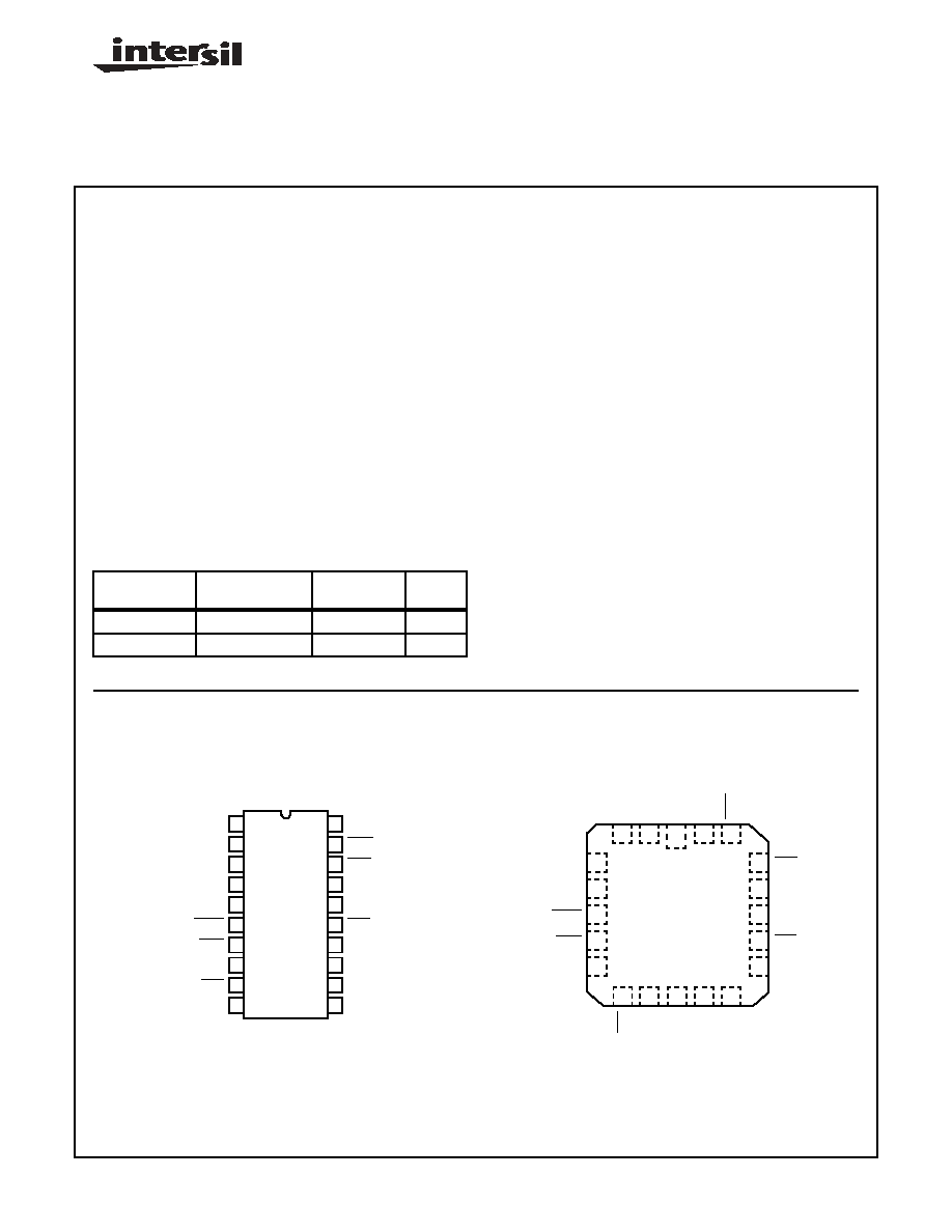
∑ Available in 20 Lead Dual-In-Line and 20 Pad LCC
Package
Description
The HD-6409/883 Manchester Encoder-Decoder (MED) is a
high speed, low power device manufactured using self-
aligned silicon gate technology. The device is intended for
use in serial data communication, and can be operated in
either of two modes. In the converter mode, the MED con-
verts Nonreturn-to-Zero code (NRZ) into Manchester code
and decodes Manchester code into Nonreturn-to-Zero code.
For serial data communication, Manchester code does not
have some of the deficiencies inherent in Nonreturn-to-Zero
code. For instance, use of the MED on a serial line elimi-
nates DC components, provides clock recovery, and gives a
relatively high degree of noise immunity. Because the MED
converts the most commonly used code (NRZ) to Manches-
ter code, the advantages of using Manchester code are eas-
ily realized in a serial data link.
In the Repeater mode, the MED accepts Manchester code
input and reconstructs it with a recovered clock. This mini-
mizes the effects of noise on a serial data link. A digital
phase lock loop generates the recovered clock. A maximum
data rate of 1MHz requires only 50mW of power.
Manchester code is used in magnetic tape recording and in
fiber optic communication, and generally is used where data
accuracy is imperative. Because it frames blocks of data, the
HD-6409/883 easily interfaces to protocol controllers.
Ordering Information
PART NUMBER
TEMPERATURE
RANGE PACKAGE
PKG.
NO.
HD1-6409/883
-55
o
C to +125
o
C
CERDIP
F20.3
HD4-6409/883
-55
o
C to +125
o
C
CLCC
J20.A
Pinouts
HD1-6409/883 (CERDIP)
TOP VIEW
HD4-6409/883 (CLCC)
TOP VIEW
11
12
13
14
15
16
17
18
20
19
10
9
8
7
6
5
4
3
2
1
BZI
BOI
UDI
SD/CDS
SDO
SRST
DCLK
NVM
RST
GND
VCC
BZO
SS
ECLK
BOO
CTS
MS
OX
IX
CO
SD/CDS
SDO
SRST
NVM
DCLK
UD
I
BO
I
BZ
I
VC
C
BO
O
RS
T
GN
D
CO
IX
OX
BZO
SS
ECLK
CTS
MS
4
5
6
7
8
10
11
12
13
9
3
2
1
20
19
16
17
18
15
14
FN2959.1
CAUTION: These devices are sensitive to electrostatic discharge; follow proper IC Handling Procedures.
1-888-INTERSIL or 321-724-7143
|
Intersil (and design) is a trademark of Intersil Americas Inc.
Copyright © Intersil Americas Inc. 2002. All Rights Reserved
136
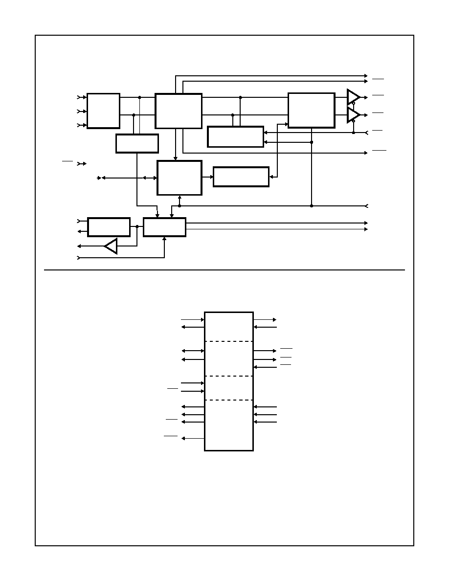
Block Diagram
Logic Symbol
MANCHESTER
ENCODER
INPUT/
OUTPUT
SELECT
EDGE
DETECTOR
COUNTER
CIRCUITS
OSCILLATOR
DATA
INPUT
LOGIC
COMMAND
SYNC
GENERATOR
5-BIT SHIFT
REGISTER
AND DECODER
BOI
BZI
UDI
RST
RESET
SD/CDS
SD
IX
OX
CO
SS
DCLK
ECLK
MS
SRST
CTS
BZO
BOO
NVM
SDO
OUTPUT
SELECT
LOGIC
CLOCK
GENERATOR
17
SS
OX
ENCODER
CONTROL
DECODER
11
4
16
14
9
5
8
7
6
CO
SD/CDS
ECLK
MS
RST
SDO
DCLK
NVM
SRST
IX
BOO
BZO
CTS
BOI
BZI
UDI
13
12
19
18
2
1
3
15
HD-6409/883

137
Absolute Maximum Ratings
Thermal Information
Supply Voltage . . . . . . . . . . . . . . . . . . . . . . . . . . . . . . . . . . . . . +7.0V
Input, Output or I/O Voltage Applied. . . . . GND -0.5V to VCC +0.5V
ESD Classification . . . . . . . . . . . . . . . . . . . . . . . . . . . . . . . . Class 1
Operating Conditions
Operating Temperature Range. . . . . . . . . . . . . . . . -55
o
C to +125
o
C
Operating Voltage Range . . . . . . . . . . . . . . . . . . . . . +4.5V to +5.5V
Input Rise and Fall Times. . . . . . . . . . . . . . . . . . . . . . . . . . 50ns Max
Sync. Transition Span (t2) . . . . . . . . . 1.5 DBP Typical, (Notes 1, 2)
Short Data Transition Span (t4) . . . . . 0.5 DBP Typical, (Notes 1, 2)
Long Data Transition Span (t5) . . . . . 1.0 DBP Typical, (Notes 1, 2)
Zero Crossing Tolerance (tCD5) . . . . . . . . . . . . . . . . . . . . . (Note 3)
Thermal Resistance
JA
(
o
C/W)
JC
(
o
C/W)
CERDIP Package . . . . . . . . . . . . . . . .
83
23
CLCC Package . . . . . . . . . . . . . . . . . .
95
26
Storage Temperature Range . . . . . . . . . . . . . . . . .-65
o
C to +150
o
C
Maximum Junction Temperature. . . . . . . . . . . . . . . . . . . . . . +175
o
C
Maximum Lead Temperature (Soldering 10s). . . . . . . . . . . . +300
o
C
Die Characteristics
Gate Count . . . . . . . . . . . . . . . . . . . . . . . . . . . . . . . . . . . . 250 Gates
CAUTION: Stresses above those listed in "Absolute Maximum Ratings" may cause permanent damage to the device. This is a stress only rating and operation
of the device at these or any other conditions above those indicated in the operational sections of this specification is not implied.
NOTES:
1. DBP - Data Bit Period. Clock Rate = 16X, one DBP = 16 Clock Cycles; Clock Rate = 32X; one DBP = 32 Clock Cycles.
2. The input conditions specified are nominal values, the actual input waveforms transition spans may vary by
±
2 IX clock cycles (16X mode)
or
±
6 IX clock cycles (32X mode).
3. The maximum zero crossing tolerance is
±
2 IX clock cycles (16X mode) or
±
6 IX clock cycles (32X mode) from the nominal.
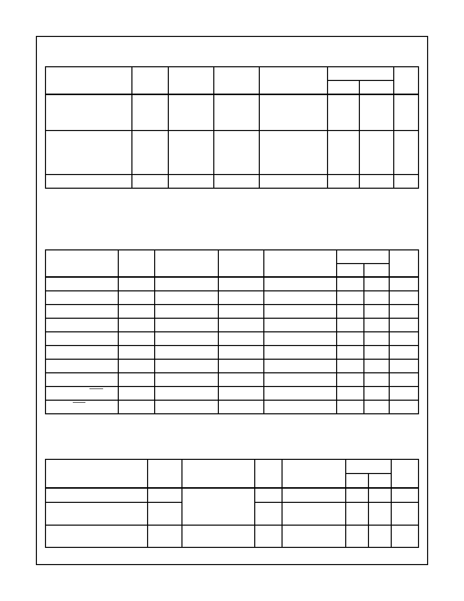
TABLE 1. HD-6409/883 DC ELECTRICAL PERFORMANCE SPECIFICATIONS
Device Guaranteed and 100% Tested
PARAMETER
SYMBOL
CONDITIONS
GROUP A
SUBGROUPS
TEMPERATURE
LIMITS
UNITS
MIN
MAX
Logic "1" Input Voltage
VIH
VCC = 4.5V
1, 2, 3
-55
o
C
T
A
+125
o
C
70%
VCC
-
V
Logic "0" Input voltage
VIL
VCC = 4.5V
1, 2, 3
-55
o
C
T
A
+125
o
C
-
20% VCC
V
Logic "1" Input Voltage
(RST)
VIHR
VCC = 5.5V
1, 2, 3
-55
o
C
T
A
+125
o
C
VCC -0.5
-
V
Logic "0" Input Voltage
(RST)
VILR
VCC = 4.5V
1, 2, 3
-55
o
C
T
A
+125
o
C
-
GND +0.5
V
Logic "1" Input Voltage (IX)
VIHC
VCC = 5.5V
1, 2, 3
-55
o
C
T
A
+125
o
C
VCC -0.5
-
V
Logic "0" Input Voltage (IX)
VlLC
VCC = 4.5V
1, 2, 3
-55
o
C
T
A
+125
o
C
-
GND +0.5
V
Input Leakage Current
(Except IX)
II
VIN = VCC or
GND
VCC = 5.5V
1, 2, 3
-55
o
C
T
A
+125
o
C
-1.0
+1.0
µ
A
Input Leakage Current
(IX)
II
VlN = VCC or
GND
VCC = 5.5V
1, 2, 3
-55
o
C
T
A
+125
o
C
-20
+20
µ
A
I/O Leakage Current
IO
VOUT = VCC
or GND
VCC = 5.5V
1, 2, 3
-55
o
C
T
A
+125
o
C
-10
+10
µ
A
Output HIGH Voltage
(All except OX)
VOH
IOH = -2.0mA
VCC = 4.5V
(Note 1)
1, 2, 3
-55
o
C
T
A
+125
o
C
VCC -0.4
-
V
Output LOW Voltage
(All except OX)
VOL
IOL = +2.0mA
VCC = 4.5V
(Note 1)
1, 2, 3
-55
o
C
T
A
+125
o
C
-
0.4
V
HD-6409/883
138
Standby Power Supply
Current
ICCSB
VIN = VCC or
GND,
VCC = 5.5V,
Outputs Open
1, 2, 3
-55
o
C
T
A
+125
o
C
-
100
µ
A
Operating Power Supply
Current
ICCOP
f = 16.0MHz,
VIN = VCC or
GND
VCC = 5.5V,
CL = 50pF
1, 2, 3
-55
o
C
T
A
+125
o
C
-
18.0
mA
Functional Test
FT
(Note 2)
7, 8
-55
o
C
T
A
+125
o
C
-
-
-
NOTES:
1. Interchanging of force and sense conditions is permitted.
2. Tested as follows: f = 16MHz, VIH = 70% VCC, VIL = 20% VCC, VOH
VCC/2, and VOL
VCC/2, VCC = 4.5V and 5.5V.
TABLE 2. HD-6409/883 AC ELECTRICAL PERFORMANCE SPECIFICATIONS
Device Guaranteed and 100% Tested
PARAMETER
SYMBOL
(NOTE 1)
CONDITIONS
GROUP A
SUBGROUPS
TEMPERATURE
LIMITS
UNITS
MIN
MAX
Clock Frequency
fC
9, 10, 11
-55
o
C
T
A
+125
o
C
-
16
MHz
Clock Period
tC
9, 10, 11
-55
o
C
T
A
+125
o
C
1/fC
-
sec
Bipolar Pulse Width
t1
9, 10, 11
-55
o
C
T
A
+125
o
C
tC +10
-
ns
One-Zero Overlap
t3
9, 10, 11
-55
o
C
T
A
+125
o
C
-
tC - 10
ns
Clock High Time
tCH
f =16.0MHz
9, 10, 11
-55
o
C
T
A
+125
o
C
20
-
ns
Clock Low Time
tCL
f =16.0MHz
9, 10, 11
-55
o
C
T
A
+125
o
C
20
-
ns
Serial Data Setup Time
tCE1
9, 10, 11
-55
o
C
T
A
+125
o
C
120
-
ns
Serial Data Hold Time
tCE2
9, 10, 11
-55
o
C
T
A
+125
o
C
0
-
ns
DCLK to SDO, NVM
tCD2
9, 10, 11
-55
o
C
T
A
+125
o
C
-
40
ns
ECLK to BZO
tR2
9, 10, 11
-55
o
C
T
A
+125
o
C
-
40
ns
NOTES:
1. AC Testing as follows: f = 4.0MHz, VIH = 70% VCC, VIL = 20% VCC, Speed Select = 16X; VOH
VCC/2, VOL
VCC/2; VCC = 4.5V
and 5.5V; Input rise and fall times driven at 1 ns/V, Output load = 50pF.
TABLE 3. HD-6409/883 ELECTRICAL PERFORMANCE SPECIFICATIONS
PARAMETER
SYMBOL
CONDITIONS
NOTES
TEMPERATURE
LIMITS
UNITS
MIN
MAX
Input Capacitance
CIN
VCC = Open, f =1MHz
All Measurements are
referenced to device
GND
1, 2
T
A
= +25
o
C
-
10
pF
I/O Capacitance
CI/O
1, 2
T
A
= +25
o
C
-
12
pF
Output Rise Time (All except CO)
tr
From 1.0 to 3.5V
CL = 50pF
1, 2
-55
o
C
T
A
+125
o
C
-
50
ns
TABLE 1. HD-6409/883 DC ELECTRICAL PERFORMANCE SPECIFICATIONS (Continued)
Device Guaranteed and 100% Tested
PARAMETER
SYMBOL
CONDITIONS
GROUP A
SUBGROUPS
TEMPERATURE
LIMITS
UNITS
MIN
MAX
HD-6409/883
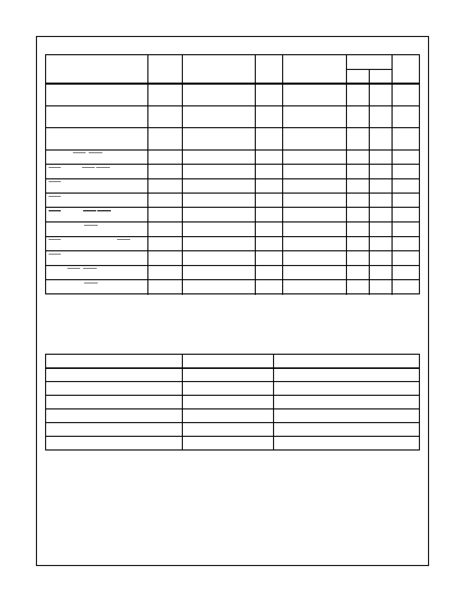
139
Output Fall Time (All except CO)
tf
From 3.5 to 1.0V
CL = 50pF
1, 2
-55
o
C
T
A
+125
o
C
-
50
ns
CO Rise Time
tr
From 1.0 to 3.5V
CL = 20pF
1, 2
-55
o
C
T
A
+125
o
C
-
11
ns
CO Fall Time
tf
From 3.5 to 1.0V
CL = 20pF
1, 2
-55
o
C
T
A
+125
o
C
-
11
ns
ECLK to BZO, BOO
tCE3
1, 3
-55
o
C
T
A
+125
o
C
0.5
1.0
DBP
CTS Low to BZO BOO Enabled
tCE4
1, 3
-55
o
C
T
A
+125
o
C
0.5
1.5
DBP
CTS Low to ECLK Enabled
tCE5
1, 3
-55
o
C
T
A
+125
o
C
10.5
11.5
DBP
CTS High to ECLK Disabled
tCE6
1, 3
-55
o
C
T
A
+125
o
C
-
1.0
DBP
CTS High to BZO BOO Disabled
tCE7
1, 3
-55
o
C
T
A
+125
o
C
1.5
2.5
DBP
UDI to SDO, NVM
tCD1
1, 3
-55
o
C
T
A
+125
o
C
2.5
3.0
DBP
RST Low to DCLK, SDO, NVM Low
tCD3
1.3
-55
o
C
T
A
+125
o
C
0.5
1.5
DBP
RST High to DCLK, Enabled
tCD4
1, 3
-55
o
C
T
A
+125
o
C
0.5
1.5
DBP
UDI to BZO, BOO
tR1
1, 3
-55
o
C
T
A
+125
o
C
0.5
1.0
DBP
UDI to SDO, NVM
tR3
1, 3
-55
o
C
T
A
+125
o
C
2.5
3.0
DBP
NOTES:
1. The parameters listed in Table 3 are controlled via design or process parameters and are not directly tested.
2. Guaranteed via characterization at initial device design and after major process and/or design changes.
3. DBP-Data Bit Period, Clock Rate = 16X, one DBP = 16 Clock Cycles; Clock Rate = 32X, one DBP = 32 Clock Cycles.
TABLE 4. APPLICABLE SUBGROUPS
CONFORMANCE GROUPS
METHOD
SUBGROUPS
Initial Test
100%/5004
-
Interim Test
100%/5004
1, 7, 9
PDA
100%
1
Final Test
100%
2, 3, 8A, 8B, 10, 11
Group A
-
1, 2, 3, 7, 8A, 8B, 9, 10, 11
Groups C & D
Samples/5005
1, 7, 9
TABLE 3. HD-6409/883 ELECTRICAL PERFORMANCE SPECIFICATIONS (Continued)
PARAMETER
SYMBOL
CONDITIONS
NOTES
TEMPERATURE
LIMITS
UNITS
MIN
MAX
HD-6409/883
140
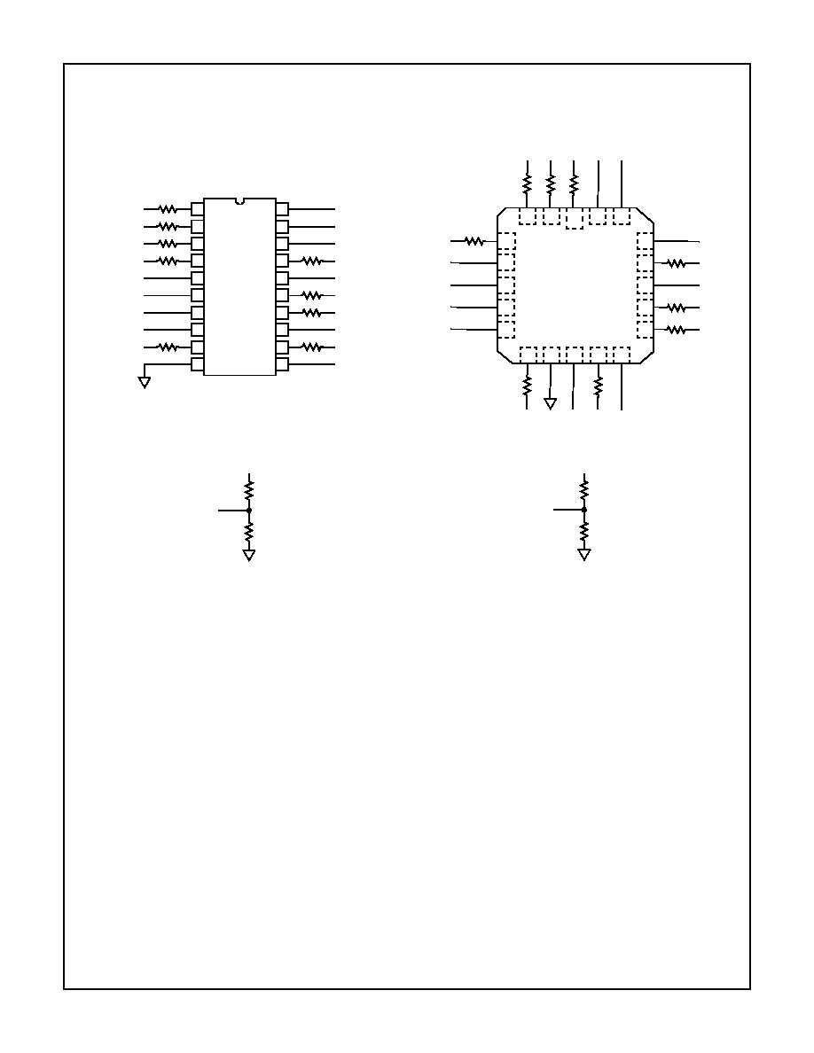
Burn-In Circuits
HD-6409/883 CERDIP
NOTES:
1. VCC = 5.5V
±
0.5V
2. VIH = 4.5V
±
10%
3. VIL = -0.2V to 0.4V
4. R1
= 47k
±
5%
5. F0
= 100kHz
±
10%
6. F4
= F0/16
HD-6409/883 CLCC
11
12
13
14
15
16
17
18
20
19
10
9
8
7
6
5
4
3
2
1
VCC
GND
F4
GND
A
A
A
A
VCC
VCC
A
A
GND
A
GND
A
GND
F0
A
VCC
A
R1
R1
R1
R1
R1
R1
R1
R1
R1
R1
R1
VCC
A
R1
R1
4
5
6
7
8
10
11
12
13
9
3
2
1
20
19
16
17
18
15
14
F4
R1
GN
D
VC
C
VC
C
A
R1
R1
GND
A
A
A
A
R1
R1
R1
A
GND
A
GND
GND
VC
C
A
F0
A
R1
R1
R1
HD-6409/883

141
Die Characteristics
DIE DIMENSIONS:
88
x 78
x 19
±
1mils
METALLIZATION:
Type: Silicon - Aluminum
Thickness: Metal 1: 8k
≈
±
1k
≈
Metal 2
:
16k
≈
±
1k
≈
GLASSIVATION:
Type: Si3N4
∑
SiOX
Thickness: 10k
≈
±
2k
≈
WORST CASE CURRENT DENSITY:
0.8 x 10
5
A/cm
2
Metallization Mask Layout
HD-6409/883
UDI
BOI
BZI
VCC
BOO
SD/CDS
SDO
SRST
NVM
DCLK
RST
GND
CO
IX
OX
MS
CTS
ECLK
SS
BZO
HD-6409/883