
5-1
March 1997
HD-6409
CMOS Manchester Encoder-Decoder
Features
∑ Converter or Repeater Mode
∑ Independent Manchester Encoder and Decoder
Operation
∑ Static to One Megabit/sec Data Rate Guaranteed
∑ Low Bit Error Rate
∑ Digital PLL Clock Recovery
∑ On Chip Oscillator
∑ Low Operating Power: 50mW Typical at +5V
∑ Available in 20 Lead Dual-In-Line and 20 Pad LCC
Package
Description
The HD-6409 Manchester Encoder-Decoder (MED) is a high
speed, low power device manufactured using self-aligned sil-
icon gate technology. The device is intended for use in serial
data communication, and can be operated in either of two
modes. In the converter mode, the MED converts Non
return-to-Zero code (NRZ) into Manchester code and
decodes Manchester code into Nonreturn-to-Zero code. For
serial data communication, Manchester code does not have
some of the deficiencies inherent in Nonreturn-to-Zero code.
For instance, use of the MED on a serial line eliminates DC
components, provides clock recovery, and gives a relatively
high degree of noise immunity. Because the MED converts
the most commonly used code (NRZ) to Manchester code,
the advantages of using Manchester code are easily realized
in a serial data link.
In the Repeater mode, the MED accepts Manchester code
input and reconstructs it with a recovered clock. This mini-
mizes the effects of noise on a serial data link. A digital
phase lock loop generates the recovered clock. A maximum
data rate of 1MHz requires only 50mW of power.
Manchester code is used in magnetic tape recording and in
fiber optic communication, and generally is used where data
accuracy is imperative. Because it frames blocks of data, the
HD-6409 easily interfaces to protocol controllers.
Pinouts
HD-6409 (CERDIP, PDIP, SOIC)
TOP VIEW
HD-6409 (CLCC)
TOP VIEW
Ordering Information
PACKAGE
TEMPERATURE
RANGE
1 MEGABIT/SEC
PKG.
NO.
PDIP
-40
o
C to +85
o
C
HD3-6409-9
E20.3
SOIC
-40
o
C to +85
o
C
HD9P6409-9
M20.3
CERDIP
-40
o
C to +85
o
C
HD1-6409-9
F20.3
DESC
-55
o
C to 125
o
C
5962-9088801MRA
F20.3
CLCC
-40
o
C to +85
o
C
HD4-6409-9
J20.A
DESC
-55
o
C to 125
o
C
5962-9088801M2A
J20.A
11
12
13
14
15
16
17
18
20
19
10
9
8
7
6
5
4
3
2
1
BZI
BOI
UDI
SD/CDS
SDO
SRST
DCLK
NVM
RST
GND
V
CC
BZO
SS
ECLK
BOO
CTS
MS
OX
IX
CO
SD/CDS
SDO
SRST
NVM
DCLK
UDI
BOI
BZI
V
CC
BOO
RST
GND
CO
IX
OX
BZO
SS
ECLK
CTS
MS
4
5
6
7
8
10
11
12
13
9
3
2
1
20
19
16
17
18
15
14
File Number
2951.1
CAUTION: These devices are sensitive to electrostatic discharge; follow proper IC Handling Procedures.
http://www.intersil.com or 407-727-9207
|
Copyright
©
Intersil Corporation 1999

5-2
Block Diagram
Logic Symbol
EDGE
DETECTOR
COMMAND
SYNC
GENERATOR
OUTPUT
SELECT
LOGIC
BOI
BZI
UDI
RST
SD/CDS
IX
OX
CO
SS
RESET
5-BIT SHIFT
REGISTER
AND DECODER
DATA
INPUT
LOGIC
INPUT/
OUTPUT
SELECT
OSCILLATOR
COUNTER
CIRCUITS
MANCHESTER
ENCODER
SDO
NVM
BOO
BZO
CTS
SRST
MS
ECLK
DCLK
SD
CLOCK
GENERATOR
ENCODER
CONTROL
DECODER
SS
CO
SD/CDS
ECLK
MS
RST
SDO
DCLK
NVM
SRST
OX
IX
BOO
BZO
CTS
BOI
BZI
UDI
13
12
19
18
15
2
1
3
17
11
4
16
14
8
7
6
5
9
HD-6409

5-3
Pin Description
PIN
NUMBER
TYPE
SYMBOL
NAME
DESCRIPTION
1
I
BZl
Bipolar Zero Input
Used in conjunction with pin 2, Bipolar One Input (BOl), to input Manchester II
encoded data to the decoder, BZI and BOl are logical complements. When using
pin 3, Unipolar Data Input (UDI) for data input, BZI must be held high.
2
I
BOl
Bipolar One Input
Used in conjunction with pin 1, Bipolar Zero Input (BZI), to input Manchester II
encoded data to the decoder, BOI and BZI are logical complements. When using
pin 3, Unipolar Data Input (UDI) for data input, BOl must be held low.
3
I
UDI
Unipolar Data Input
An alternate to bipolar input (BZl, BOl), Unipolar Data Input (UDl) is used to input
Manchester II encoded data to the decoder. When using pin 1 (BZl) and pin 2
(BOl) for data input, UDI must be held low.
4
I/O
SD/CDS
Serial Data/Com-
mand Data Sync
In the converter mode, SD/CDS is an input used to receive serial NRZ data. NRZ
data is accepted synchronously on the falling edge of encoder clock output
(ECLK). In the repeater mode, SD/CDS is an output indicating the status of last
valid sync pattern received. A high indicates a command sync and a low indicates
a data sync pattern.
5
O
SDO
Serial Data Out
The decoded serial NRZ data is transmitted out synchronously with the decoder
clock (DCLK). SDO is forced low when RST is low.
6
O
SRST
Serial Reset
In the converter mode, SRST follows RST. In the repeater mode, when RST goes
low, SRST goes low and remains low after RST goes high. SRST goes high only
when RST is high, the reset bit is zero, and a valid synchronization sequence is
received.
7
O
NVM
Nonvalid Manchester
A low on NVM indicates that the decoder has received invalid Manchester data
and present data on Serial Data Out (SDO) is invalid. A high indicates that the
sync pulse and data were valid and SDO is valid. NVM is set low by a low on RST,
and remains low after RST goes high until valid sync pulse followed by two valid
Manchester bits is received.
8
O
DCLK
Decoder Clock
The decoder clock is a 1X clock recovered from BZl and BOl, or UDI to synchro-
nously output received NRZ data (SDO).
9
I
RST
Reset
In the converter mode, a low on RST forces SDO, DCLK, NVM, and SRST low.
A high on RST enables SDO and DCLK, and forces SRST high. NVM remains
low after RST goes high until a valid sync pulse followed by two Manchester bits
is received, after which it goes high. In the repeater mode, RST has the same ef-
fect on SDO, DCLK and NVM as in the converter mode. When RST goes low,
SRST goes low and remains low after RST goes high. SRST goes high only
when RST is high, the reset bit is zero and a valid synchronization sequence is
received.
10
I
GND
Ground
Ground
11
O
C
O
Clock Output
Buffered output of clock input I
X
. May be used as clock signal for other peripherals.
12
I
I
X
Clock Input
I
X
is the input for an external clock or, if the internal oscillator is used, I
X
and O
X
are used for the connection of the crystal.
13
O
O
X
Clock Drive
If the internal oscillator is used, O
X
and I
X
are used for the connection of the crys-
tal.
14
I
MS
Mode Select
MS must be held low for operation in the converter mode, and high for operation
in the repeater mode.
15
I
CTS
Clear to Send
In the converter mode, a high disables the encoder, forcing outputs BOO, BZO high
and ECLK low. A high to low transition of CTS initiates transmission of a Command
sync pulse. A low on CTS enables BOO, BZO, and ECLK. In the repeater mode,
the function of CTS is identical to that of the converter mode with the exception that
a transition of CTS does not initiate a synchronization sequence.
16
O
ECLK
Encoder Clock
In the converter mode, ECLK is a 1X clock output used to receive serial NRZ data
to SD/CDS. In the repeater mode, ECLK is a 2X clock which is recovered from
BZl and BOl data by the digital phase locked loop.
HD-6409
5-4
Encoder Operation
The encoder uses free running clocks at 1X and 2X the data
rate derived from the system clock l
X
for internal timing. CTS
is used to control the encoder outputs, ECLK, BOO and
BZO. A free running 1X ECLK is transmitted out of the
encoder to drive the external circuits which supply the NRZ
data to the MED at pin SD/CDS.
A low on CTS enables encoder outputs ECLK, BOO and
BZO, while a high on CTS forces BZO, BOO high and holds
ECLK low. When CTS goes from high to low
, a synchro-
nization sequence is transmitted out on BOO and BZO. A
synchronization sequence consists of eight Manchester "0"
bits followed by a command sync pulse.
A command
sync pulse is a 3-bit wide pulse with the first 1 1/2 bits high
followed by 1 1/2 bits low.
Serial NRZ data is clocked into
the encoder at SD/CDS on the high to low transition of ECLK
during the command sync pulse. The NRZ data received is
encoded into Manchester II data and transmitted out on
BOO and BZO following the command sync pulse.
Fol-
lowing the synchronization sequence, input data is encoded
and transmitted out continuously without parity check or
word framing. The length of the data block encoded is
defined by CTS. Manchester data out is inverted.
Decoder Operation
The decoder requires a single clock with a frequency 16X or
32X the desired data rate. The rate is selected on the speed
select with SS low producing a 16X clock and high a 32X
clock. For long data links the 32X mode should be used as
this permits a wider timing jitter margin. The internal opera-
tion of the decoder utilizes a free running clock synchronized
with incoming data for its clocking.
The Manchester II encoded data can be presented to the
decoder in either of two ways. The Bipolar One and Bipolar
Zero inputs will accept data from differential inputs such as a
comparator sensed transformer coupled bus. The Unipolar
Data input can only accept noninverted Manchester II
encoded data i.e. Bipolar One Out through an inverter to
Unipolar Data Input. The decoder continuously monitors this
data input for valid sync pattern. Note that while the MED
encoder section can generate only a command sync pattern,
the decoder can recognize either a command or data sync
pattern. A data sync is a logically inverted command sync.
17
I
SS
Speed Select
A logic high on SS sets the data rate at 1/32 times the clock frequency while a
low sets the data rate at 1/16 times the clock frequency.
18
O
BZO
Bipolar Zero Output
BZO and its logical complement BOO are the Manchester data outputs of the en-
coder. The inactive state for these outputs is in the high state.
19
O
BOO
Bipolar One Out
See pin 18.
20
I
V
CC
V
CC
V
CC
is the +5V power supply pin. A 0.1
µ
F decoupling capacitor from V
CC
(pin-
20) to GND (pin-10) is recommended.
NOTE: (I) Input
(O) Output
Pin Description
PIN
NUMBER
TYPE
SYMBOL
NAME
DESCRIPTION
1
2
3
4
1
2
3
4
CTS
ECLK
SD/CDS
BZO
BOO
t
CE6
0
0
0
0
0
0
0
0
t
CE5
SYNCHRONIZATION SEQUENCE
EIGHT "0's"
COMMAND
SYNC
DON'T CARE
`1'
`0'
`1'
`1'
`0' `1'
FIGURE 1. ENCODER OPERATION
HD-6409
5-5
There is a three bit delay between UDI, BOl, or BZI input and
the decoded NRZ data transmitted out of SDO.
Control of the decoder outputs is provided by the RST pin.
When RST is low, SDO, DCLK and NVM are forced low.
When RST is high, SDO is transmitted out synchronously
with the recovered clock DCLK. The NVM output remains
low after a low to high transition on RST until a valid sync
pattern is received.
The decoded data at SDO is in NRZ format. DCLK is pro-
vided so that the decoded bits can be shifted into an external
register on every high to low transition of this clock. Three bit
periods after an invalid Manchester bit is received on UDI, or
BOl, NVM goes low synchronously with the questionable
data output on SDO. FURTHER, THE DECODER DOES
NOT REESTABLISH PROPER DATA DECODING UNTIL
ANOTHER SYNC PATTERN IS RECOGNIZED.
Repeater Operation
Manchester Il data can be presented to the repeater in either
of two ways. The inputs Bipolar One In and Bipolar Zero In
will accept data from differential inputs such as a comparator
or sensed transformer coupled bus. The input Unipolar Data
In accepts only noninverted Manchester II coded data. The
decoder requires a single clock with a frequency 16X or 32X
the desired data rate. This clock is selected to 16X with
Speed Select low and 32X with Speed Select high. For long
data links the 32X mode should be used as this permits a
wider timing jitter margin.
The inputs UDl, or BOl, BZl are delayed approximately 1/2
bit period and repeated as outputs BOO and BZO. The 2X
ECLK is transmitted out of the repeater synchronously with
BOO and BZO.
A low on CTS enables ECLK, BOO, and BZO. In contrast to
the converter mode, a transition on CTS does not initiate a
synchronization sequence of eight 0's and a command sync.
The repeater mode does recognize a command or data sync
pulse. SD/CDS is an output which reflects the state of the
most recent sync pulse received, with high indicating a com-
mand sync and low indicating a data sync.
When RST is low, the outputs SDO, DCLK, and NVM are
low, and SRST is set low. SRST remains low after RST goes
high and is not reset until a sync pulse and two valid
manchester bits are received with the reset bit low. The reset
bit is the first data bit after the sync pulse. With RST high,
NRZ Data is transmitted out of Serial Data Out synchro-
nously with the 1X DCLK.
FIGURE 2. DECODER OPERATION
DCLK
UDI
SDO
RST
NVM
COMMAND
SYNC
1
0
0
1
0
1
0
1
0
1
0
1
0
FIGURE 3. REPEATER OPERATION
INPUT
COUNT
ECLK
UDI
BZO
BOO
RST
SRST
SYNC PULSE
1
2
3
4
5
6
7
HD-6409

5-6
Manchester Code
Nonreturn-to-Zero (NRZ) code represents the binary values
logic-O and Iogic-1 with a static level maintained throughout
the data cell. In contrast, Manchester code represents data
with a level transition in the middle of the data cell. Manches-
ter has bandwidth, error detection, and synchronization
advantages over NRZ code.
The Manchester II code Bipolar One and Bipolar Zero shown
below are logical complements. The direction of the transi-
tion indicates the binary value of data. A logic-0 in Bipolar
One is defined as a Low to high transition in the middle of
the data cell, and a logic-1 as a high to low mid bit transition,
Manchester Il is also known as Biphase-L code.
The bandwidth of NRZ is from DC to the clock frequency fc/2,
while that of Manchester is from fc/2 to fc. Thus, Manchester
can be AC or transformer coupled, which has considerable
advantages over DC coupling. Also, the ratio of maximum to
minimum frequency of Manchester extends one octave, while
the ratio for NRZ is the range of 5-10 octaves. It is much eas-
ier to design a narrow band than a wideband amp.
Secondly, the mid bit transition in each data cell provides the
code with an effective error detection scheme. If noise pro-
duces a logic inversion in the data cell such that there is no
transition, an error indiction is given, and synchronization
must be re-established. This places relatively stringent
requirements on the incoming data.
The synchronization advantages of using the HD-6409 and
Manchester code are several fold. One is that Manchester is
a self clocking code. The clock in serial data communication
defines the position of each data cell. Non self clocking
codes, as NRZ, often require an extra clock wire or clock
track (in magnetic recording). Further, there can be a phase
variation between the clock and data track. Crosstalk
between the two may be a problem. In Manchester, the
serial data stream contains both the clock and the data, with
the position of the mid bit transition representing the clock,
and the direction of the transition representing data. There is
no phase variation between the clock and the data.
A second synchronization advantage is a result of the num-
ber of transitions in the data. The decoder resynchronizes on
each transition, or at least once every data cell. In contrast,
receivers using NRZ, which does not necessarily have tran-
sitions, must resynchronize on frame bit transitions, which
occur far less often, usually on a character basis. This more
frequent resynchronization eliminates the cumulative effect
of errors over successive data cells. A final synchronization
advantage concerns the HD-6409's sync pulse used to ini-
tiate synchronization. This three bit wide pattern is suffi-
ciently distinct from Manchester data that a false start by the
receiver is unlikely.
Crystal Oscillator Mode
FIGURE 5. CRYSTAL OSCILLATOR MODE
LC Oscillator Mode
FIGURE 6. LC OSCILLATOR MODE
FIGURE 4. MANCHESTER CODE
BIT PERIOD
BINARY CODE
NONRETURN
TO ZERO
BIPOLAR ONE
BIPOLAR ZERO
1
2
3
4
5
0
1
1
0
0
I
X
O
X
X1
R1
C0
16MHz
C1
C1
C
O
C1 = 32pF
C0 = CRYSTAL + STRAY
X1 = AT CUT PARALLEL
RESONANCE
FUNDAMENTAL
MODE
R
S
(TYP) = 30
R1 = 15M
C1
C1
L
C
E
C1
2C0
≠
2
--------------------------
f
O
1
2
LC
e
-----------------------
C1 = 20pF
C0 = 5pF
I
X
O
X
HD-6409
5-7
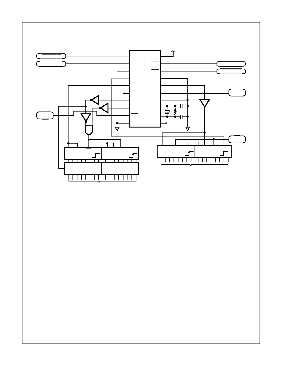
Using the 6409 as a Manchester Encoded UART
V
CC
BOO
BZO
SS
ECLK
CTS
MS
OX
IX
CO
BZI
BOI
UDI
SD/CDS
SDO
SRST
NVM
DCLK
RST
GND
BIPOLAR OUT
BIPOLAR OUT
CTS
LOAD
LOAD
QH
CK
SI
`165
LOAD
QH
CK
`165
B
QH
A
`164
B
CK
A
`164
CK
DATA IN
`273
DATA IN
`273
CP
RESET
BIPOLAR IN
BIPOLAR IN
FIGURE 7. MANCHESTER ENCODER UART
PARALLEL DATA OUT
PARALLEL DATA IN
HD-6409

5-8
Absolute Maximum Ratings
Thermal Information
Supply Voltage . . . . . . . . . . . . . . . . . . . . . . . . . . . . . . . . . . . . . +7.0V
Input, Output or I/O Voltage . . . . . . . . . . . GND -0.5V to V
CC
+0.5V
ESD Classification . . . . . . . . . . . . . . . . . . . . . . . . . . . . . . . . Class 1
Thermal Resistance (Typical)
JA
JC
CERDIP . . . . . . . . . . . . . . . . . . . . . . . . . .
83
o
C/W
23
o
C/W
CLCC Package . . . . . . . . . . . . . . . . . . . .
95
o
C/W
26
o
C/W
PDIP Package . . . . . . . . . . . . . . . . . . . . .
75
o
C/W
N/A
SOIC Package . . . . . . . . . . . . . . . . . . . . .
100
o
C/W
N/A
Storage Temperature Range . . . . . . . . . . . . . . . . . .-65
o
C to +150
o
C
Maximum Junction Temperature
Ceramic Package . . . . . . . . . . . . . . . . . . . . . . . . . . . . . . . +175
o
C
Plastic Package . . . . . . . . . . . . . . . . . . . . . . . . . . . . . . . . . +150
o
C
Maximum Lead Temperature (Soldering 10s) . . . . . . . . . . . . +300
o
C
(
Lead Tips Only for Surface Mount Packages)
Die Characteristics
Gate Count . . . . . . . . . . . . . . . . . . . . . . . . . . . . . . . . . . . . 250 Gates
CAUTION: Stresses above those listed in "Absolute Maximum Ratings" may cause permanent damage to the device. This is a stress only rating and operation
of the device at these or any other conditions above those indicated in the operational sections of this specification is not implied.
Operating Conditions
Operating Temperature Range . . . . . . . . . . . . . . . . . -40
o
C to +85
o
C
Operating Voltage Range . . . . . . . . . . . . . . . . . . . . . +4.5V to +5.5V
Input Rise and Fall Times . . . . . . . . . . . . . . . . . . . . . . . . . .50ns Max
Sync. Transition Span (t2) . . . . . . . . . . 1.5 DBP Typical, (Notes 1, 2)
Short Data Transition Span (t4). . . . . . .0.5DBP Typical, (Notes 1, 2)
Long Data Transition Span (t5) . . . . . . .1.0DBP Typical, (Notes 1, 2)
Zero Crossing Tolerance (tCD5) . . . . . . . . . . . . . . . . . . . . . .(Note 3)
NOTES:
1. DBP-Data Bit Period, Clock Rate = 16X, one DBP = 16 Clock Cycles; Clock Rate = 32X, one DBP = 32 Clock Cycles.
2. The input conditions specified are nominal values, the actual input waveforms transition spans may vary by
±
2 I
X
clock cycles (16X mode)
or
±
6 I
X
clock cycles (32X mode).
3. The maximum zero crossing tolerance is
±
2 I
X
clock cycles (16X mode) or
±
6 I
X
clock cycles (32 mode) from the nominal.
DC Electrical Specifications
V
CC
= 5.0V
±
10%, T
A
= -40
o
C to +85
o
(HD-6409-9)
SYMBOL
PARAMETER
MIN
MAX
UNITS
(NOTE 1) TEST CONDITIONS
V
IH
Logical "1" Input Voltage
70% V
CC
-
V
V
CC
= 4.5V
V
IL
Logical "0" Input Voltage
-
20% V
CC
V
V
CC
= 4.5V
V
IHR
Logic "1" Input Voltage (Reset)
V
CC
-0.5
-
V
V
CC
= 5.5V
V
ILR
Logic "0" Input Voltage (Reset)
-
GND +0.5
V
V
CC
= 4.5V
V
IHC
Logical "1" Input Voltage (Clock)
V
CC
-0.5
-
V
V
CC
= 5.5V
V
ILC
Logical "0" Input Voltage (Clock)
-
GND +0.5
V
V
CC
= 4.5V
I
I
Input Leakage Current (Except I
X
)
-1.0
+1.0
µ
A
V
IN
= V
CC
or GND, V
CC
= 5.5V
I
I
Input Leakage Current (I
X
)
-20
+20
µ
A
V
IN
= V
CC
or GND, V
CC
= 5.5V
I
O
I/O Leakage Current
-10
+10
µ
A
V
OUT
= V
CC
or GND, V
CC
= 5.5V
V
OH
Output HIGH Voltage (All Except O
X
)
V
CC
-0.4
-
V
I
OH
= -2.0mA, V
CC
= 4.5V (Note 2)
V
OL
Output LOW Voltage (All Except O
X
)
-
0.4
V
I
OL
= +2.0mA, V
CC
= 4.5V (Note 2)
I
CCSB
Standby Power Supply Current
-
100
µ
A
V
IN
= V
CC
or GND, V
CC
= 5.5V,
Outputs Open
I
CCOP
Operating Power Supply Current
-
18.0
mA
f = 16.0MHz, V
IN
= V
CC
or GND
V
CC
= 5.5V, C
L
= 50pF
F
T
Functional Test
-
-
-
(Note 1)
NOTES:
1. Tested as follows: f = 16MHz, V
IH
= 70% V
CC
, V
IL
= 20% V
CC
, V
OH
V
CC
/2, and V
OL
V
CC
/2, V
CC
= 4.5V and 5.5V.
2. Interchanging of force and sense conditions is permitted
Capacitance
T
A
= +25
o
C, Frequency = 1MHz
SYMBOL
PARAMETER
TYP
UNITS
TEST CONDITIONS
C
IN
Input Capacitance
10
pF
All measurements are referenced to device GND
C
OUT
Output Capacitance
12
pF
HD-6409
5-9
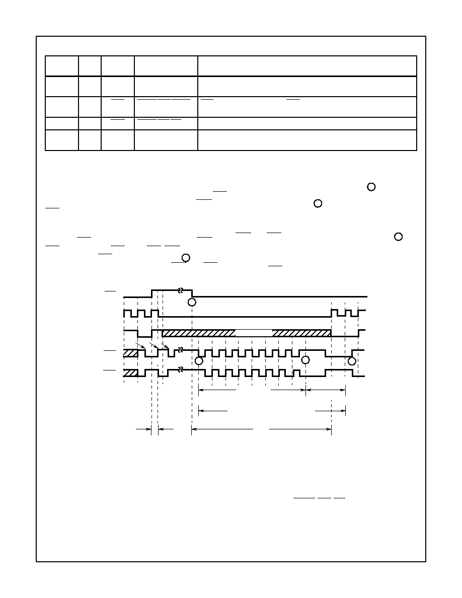
AC Electrical Specifications
V
CC
= 5.0V
±
10%, T
A
= -40
o
C to +85
o
C (HD-6409-9)
SYMBOL
PARAMETER
MIN
MAX
UNITS
(NOTE 1) TEST CONDITIONS
f
C
Clock Frequency
-
16
MHz
-
t
C
Clock Period
1/f
C
-
sec
-
t
1
Bipolar Pulse Width
t
C
+10
-
ns
-
t
3
One-Zero Overlap
-
t
C
-10
ns
-
t
CH
Clock High Time
20
-
ns
f = 16.0MHz
t
CL
Clock Low Time
20
-
ns
f = 16.0MHz
t
CE1
Serial Data Setup Time
120
-
ns
-
t
CE2
Serial Data Hold Time
0
-
ns
-
t
CD2
DCLK to SDO, NVM
-
40
ns
-
t
R2
ECLK to BZO
-
40
ns
-
t
r
Output Rise Time (All except Clock)
-
50
ns
From 1.0V to 3.5V, C
L
= 50pF, Note 2
t
f
Output Fall Time (All except Clock)
-
50
ns
From 3.5V to 1.0V, C
L
= 50pF, Note 2
t
r
Clock Output Rise Time
-
11
ns
From 1.0V to 3.5V, C
L
= 20pF, Note 2
t
f
Clock Output Fall Time
-
11
ns
From 3.5V to 1.0V, C
L
= 20pF, Note 2
t
CE3
ECLK to BZO, BOO
0.5
1.0
DBP
Notes 2, 3
t
CE4
CTS Low to BZO, BOO Enabled
0.5
1.5
DBP
Notes 2, 3
t
CE5
CTS Low to ECLK Enabled
10.5
11.5
DBP
Notes 2, 3
t
CE6
CTS High to ECLK Disabled
-
1.0
DBP
Notes 2, 3
t
CE7
CTS High to BZO, BOO Disabled
1.5
2.5
DBP
Notes 2, 3
t
CD1
UDI to SDO, NVM
2.5
3.0
DBP
Notes 2, 3
t
CD3
RST Low to CDLK, SDO, NVM Low
0.5
1.5
DBP
Notes 2, 3
t
CD4
RST High to DCLK, Enabled
0.5
1.5
DBP
Notes 2, 3
t
R1
UDI to BZO, BOO
0.5
1.0
DBP
Notes 2, 3
t
R3
UDI to SDO, NVM
2.5
3.0
DBP
Notes 2, 3
NOTES:
1. AC testing as follows: f = 4.0MHz, V
IH
= 70% V
CC
, V
IL
= 20% V
CC
, Speed Select = 16X, V
OH
V
CC
/2, V
OL
V
CC
/2, V
CC
= 4.5V and
5.5V. Input rise and fall times driven at 1ns/V, Output load = 50pF.
2. Guaranteed via characteristics at initial device design and after major process and/or design changes, not tested.
3. DBP-Data Bit Period, Clock Rate = 16X, one DBP = 16 Clock Cycles; Clock Rate = 32X, one DBP = 32 Clock Cycles.
HD-6409
5-10
Timing Waveforms
FIGURE 8.
FIGURE 9. CLOCK TIMING
FIGURE 10. OUTPUT WAVEFORM
DATA SYNC
BIT PERIOD
BIT PERIOD
BIT PERIOD
T
2
COMMAND SYNC
T
2
T
3
T
3
T
2
T
2
T
4
ONE
ONE
ZERO
T
1
T
1
T
1
T
3
T
3
T
1
T
1
T
1
T
3
T
3
T
3
T
3
T
1
T
4
T
5
T
5
T
2
T
2
COMMAND SYNC
T
2
T
2
T
4
T
5
T
5
T
4
T
4
ZERO
ONE
ONE
ONE
DATA SYNC
BOI
BZI
BOI
BZI
BOI
BZI
UDI
UDI
UDI
T
3
NOTE: UDI = 0, FOR NEXT DIAGRAMS
NOTE: BOI = 0, BZI = 1 FOR NEXT DIAGRAMS
t
C
t
CH
t
r
t
CL
t
f
10%
90%
t
r
t
f
1.0V
3.5V
HD-6409

5-11
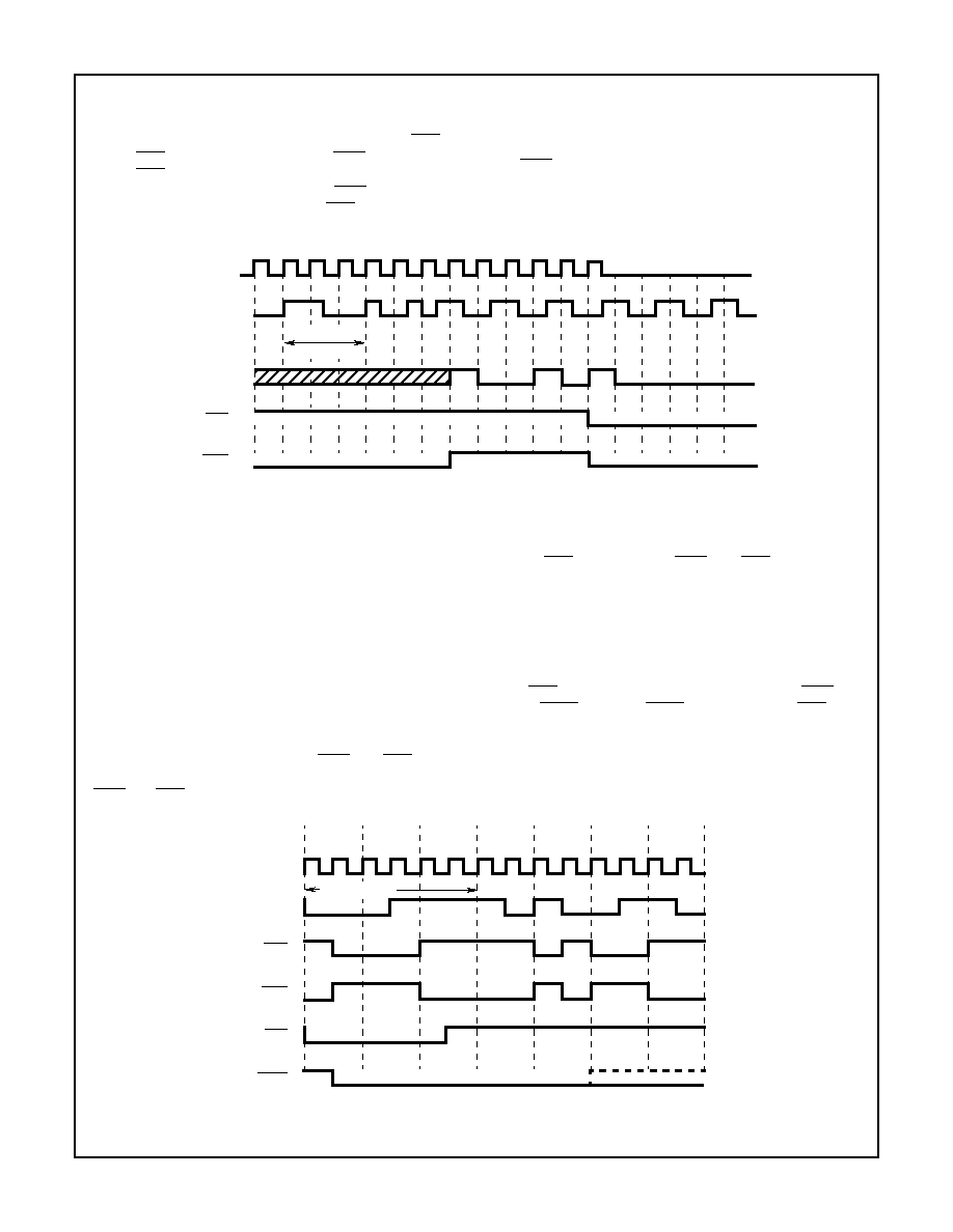
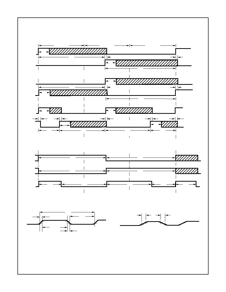
FIGURE 11. ENCODER TIMING
FIGURE 12. ENCODER TIMING
FIGURE 13. ENCODER TIMING
NOTE: Manchester Data-In is not synchronous with Decoder Clock.
Decoder Clock is synchronous with decoded NRZ out of SDO.
FIGURE 14. DECODER TIMING
FIGURE 15. DECODER TIMING
FIGURE 16. DECODER TIMING
Timing Waveforms
(Continued)
ECLK
SD/CDS
BZO
BOO
t
CE1
t
CE2
t
CE3
t
CE5
t
CE4
CTS
BZO
BOO
ECLK
t
CE6
CTS
BZO
BOO
ECLK
t
CE7
DCLK
UDI
SDO
NVM
MANCHESTER
LOGIC-1
MANCHESTER
LOGIC-0
MANCHESTER
LOGIC-0
MANCHESTER
LOGIC-1
t
CD2
t
CD5
t
CD2
t
CD1
NRZ
LOGIC-1
RST
DCLK, SDO,
NVM
50%
50%
t
CD3
RST
DCLK
50%
t
CD4
HD-6409

5-12
All Intersil semiconductor products are manufactured, assembled and tested under ISO9000 quality systems certification.
Intersil products are sold by description only. Intersil Corporation reserves the right to make changes in circuit design and/or specifications at any time without
notice. Accordingly, the reader is cautioned to verify that data sheets are current before placing orders. Information furnished by Intersil is believed to be accurate
and reliable. However, no responsibility is assumed by Intersil or its subsidiaries for its use; nor for any infringements of patents or other rights of third parties which
may result from its use. No license is granted by implication or otherwise under any patent or patent rights of Intersil or its subsidiaries.
For information regarding Intersil Corporation and its products, see web site http://www.intersil.com
Sales Office Headquarters
NORTH AMERICA
Intersil Corporation
P. O. Box 883, Mail Stop 53-204
Melbourne, FL 32902
TEL: (407) 724-7000
FAX: (407) 724-7240
EUROPE
Intersil SA
Mercure Center
100, Rue de la Fusee
1130 Brussels, Belgium
TEL: (32) 2.724.2111
FAX: (32) 2.724.22.05
ASIA
Intersil (Taiwan) Ltd.
Taiwan Limited
7F-6, No. 101 Fu Hsing North Road
Taipei, Taiwan
Republic of China
TEL: (886) 2 2716 9310
FAX: (886) 2 2715 3029
Test Load Circuit
FIGURE 17. REPEATER TIMING
Timing Waveforms
(Continued)
UDI
ECLK
BZO
SDO
NVM
MANCHESTER `1'
t
R2
t
R3
t
R3
t
R2
t
R1
MANCHESTER `0'
MANCHESTER `0'
MANCHESTER `1'
MANCHESTER `1'
MANCHESTER `0'
MANCHESTER `0'
FIGURE 18. TEST LOAD CIRCUIT
DUT
C
L
(NOTE)
NOTE: INCLUDES STRAY AND JIG
CAPACITANCE
HD-6409