Äîêóìåíòàöèÿ è îïèñàíèÿ www.docs.chipfind.ru
1
®
CAUTION: These devices are sensitive to electrostatic discharge; follow proper IC Handling Procedures.
1-888-INTERSIL or 321-724-7143
|
Intersil (and design) is a registered trademark of Intersil Americas Inc.
Copyright © Intersil Americas Inc. 2002. All Rights Reserved
HFA-0001
Ultra High Slew RateOperational Amplifier
The HFA-0001 is an all bipolar op amp featuring high slew
rate (1000V/
µ
s), and high unity gain bandwidth (350MHz).
These features combined with fast settling time (25ns) make
this product very useful in high speed data acquisition
systems as well as RF, video, and pulse amplifier designs.
Other outstanding characteristics include low bias currents
(15
µ
A), low offset current (18
µ
A), and low offset voltage
(6mV).
The HFA-0001 offers high performance at low cost. It can
replace hybrids and RF transistor amplifiers, simplifying
designs while providing increased reliability due to
monolithic construction. To enhance the ease of design, the
HFA-0001 has a 50
±
20% resistor connected from the
output of the op amp to a separate pin. This can be used
when driving 50
strip line, microstrip, or coax cable.
Features
· Unity Gain Bandwidth. . . . . . . . . . . . . . . . . . . . . . 350MHz
· Full Power Bandwidth . . . . . . . . . . . . . . . . . . . . . . 53MHz
· High Slew Rate . . . . . . . . . . . . . . . . . . . . . . . . . 1000V/
µ
s
· High Output Drive
. . . . . . . . . . . . . . . . . . . . . . . . . . . . . ±
50mA
· Monolithic Construction
Applications
· RF/IF Processors
· Video Amplifiers
· High Speed Cable Drivers
· Pulse Amplifiers
· High Speed Communications
· Fast Data Acquisition Systems
Pinouts
Part Number Information
PART
NUMBER
TEMPERATURE
RANGE
PACKAGE
HFA1-0001-5
0
o
C to +75
o
C
14 Lead Ceramic Sidebraze DIP
HFA1-0001-9
-40
o
C to +85
o
C 14 Lead Ceramic Sidebraze DIP
HFA3-0001-5
0
o
C to +75
o
C
8 Lead Plastic DIP
HFA3-0001-9
-40
o
C to +85
o
C 8 Lead Plastic DIP
HFA9P0001-5
0
o
C to +75
o
C
16 Lead Widebody SOIC
HFA-0001
(PDIP)
TOP VIEW
HFA-0001
(CDIP)
TOP VIEW
HFA-0001
(300 MIL SOIC)
TOP VIEW
NC
+IN
V-
2
3
4
1
R
SENSE
V+
OUT
NC
7
6
5
8
+
-IN
NC
NC
NC
+IN
NC
NC
NC
V+
NC
NC
1
2
3
4
5
6
7
14
13
12
11
10
9
8
R
SENSE
OUT
+
-IN
V-
14
15
16
9
13
12
11
10
1
2
3
4
5
7
6
8
NC
NC
NC
-IN
+IN
V-
NC
NC
NC
R
SENSE
V+
OUT
NC
NC
NC
NC
+
September 1998
File Number 2916.3
OBSOL
ETE PR
ODUCT
Recom
mende
d Repla
cemen
ts: HFA
1100, H
FA1105
or cont
act our
Techn
ical Su
pport C
enter a
t
1-888-I
NTERS
IL or w
ww.int
ersil.co
m/tsc
2
Absolute Maximum Ratings
(Note 1)
Operating Conditions
Supply Voltage (Between V+ and V- Terminals) . . . . . . . . . . . . .12V
Differential Input Voltage . . . . . . . . . . . . . . . . . . . . . . . . . . . . . . . .5V
Input Voltage
. . . . . . . . . . . . . . . . . . . . . . . . . . . . . . . . . . . . . . . . . . . . ±
4V
Output Current . . . . . . . . . . . . . . . . . . . . . . . . . . . . . . . . . . . . . 60mA
Junction Temperature (Note 9) . . . . . . . . . . . . . . . . . . . . . . .+175
o
C
Junction Temperature (Plastic Package) . . . . . . . . . . . . . . . .+150
o
C
Lead Temperature (Soldering 10 Sec.) . . . . . . . . . . . . . . . . .+300
o
C
Operating Temperature Range
HFA-0001-9 . . . . . . . . . . . . . . . . . . . . . . . . . .-40
o
C
T
A
+85
o
C
HFA-0001-5 . . . . . . . . . . . . . . . . . . . . . . . . . . . 0
o
C
T
A
+75
o
C
Storage Temperature Range . . . . . . . . . . . . . .-65
o
C
T
A
+150
o
C
CAUTION: Stresses above those listed in "Absolute Maximum Ratings" may cause permanent damage to the device. This is a stress only rating and operation of the
device at these or any other conditions above those indicated in the operational sections of this specification is not implied.
Electrical Specifications
V+ = +5V, V- = -5V, Unless Otherwise Specified
PARAMETER
TEMP
HFA-0001-9
HFA-0001-5
UNITS
MIN
TYP
MAX
MIN
TYP
MAX
INPUT CHARACTERISTICS
Offset Voltage
+25
o
C
-
6
15
-
6
30
mV
High
-
4.5
20
-
4.5
30
mV
Low
-
12.5
45
-
12.5
35
mV
Average Offset Voltage Drift
High
-
50
-
-
50
-
µ
V/
o
C
Low
-
100
-
-
100
-
µ
V/
o
C
Bias Current
+25
o
C
-
15
50
-
15
100
µ
A
Full
-
20
50
-
20
100
µ
A
Offset Current
+25
o
C
-
18
25
-
18
50
µ
A
Full
-
22
50
-
22
50
µ
A
Common Mode Range
+25
o
C
±
3
-
-
±
3
-
-
V
Differential Input Resistance
+25
o
C
-
10
-
-
10
-
k
Input Capacitance
+25
o
C
-
2
-
-
2
-
pF
Input Noise Voltage
0.1Hz to 10Hz
+25
o
C
-
3.5
-
-
3.5
-
µ
Vrms
10Hz to 1MHz
+25
o
C
-
6.7
-
-
6.7
-
µ
Vrms
Input Noise Voltage
f
O
= 10Hz
+25
o
C
-
640
-
-
640
-
nV/
Hz
f
O
= 100Hz
+25
o
C
-
170
-
-
170
-
nV/
Hz
f
O
= 100kHz
+25
o
C
-
6
-
-
6
-
nV/
Hz
Input Noise Current
f
O
= 10Hz
+25
o
C
-
2.35
-
-
2.35
-
nA/
Hz
f
O
= 100Hz
+25
o
C
-
0.57
-
-
0.57
-
nA/
Hz
f
O
= 1000Hz
+25
o
C
-
0.16
-
-
0.16
-
nA/
Hz
TRANSFER CHARACTERISTICS
Large Signal Voltage Gain (Note 2)
+25
o
C
150
200
-
150
200
-
V/V
High
150
170
-
100
170
-
V/V
Low
150
220
-
150
220
-
V/V
Common Mode Rejection Ratio (Note 3)
+25
o
C
45
47
-
42
47
-
dB
High
40
45
-
40
45
-
dB
Low
45
48
-
42
48
-
dB
Unity Gain Bandwidth
+25
o
C
-
350
-
-
350
-
MHz
Minimum Stable Gain
Full
1
-
-
1
-
-
V/V
OUTPUT CHARACTERISTICS
Output Voltage Swing
R
L
= 100
+25
o
C
-
±
3.5
-
-
±
3.5
-
V
HFA-0001
3
R
L
= 1k
+25
o
C
±
3.5
±
3.7
-
±
3.5
±
3.7
-
V
High
±
3.0
±
3.6
-
±
3.0
±
3.6
-
V
Low
±
3.5
±
3.7
-
±
3.5
±
3.7
-
V
Full Power Bandwidth (Note 5)
+25
o
C
-
53
-
-
53
-
MHz
Output Resistance, Open Loop
+25
o
C
-
3
-
-
3
-
Output Current
Full
±
30
±
50
-
±
30
±
50
-
mA
TRANSIENT RESPONSE
Rise Time (Note 4, 6)
+25
o
C
-
480
-
-
480
-
ps
Slew Rate (Note 4, 7)
R
L
= 1k
+25
o
C
-
1000
-
-
1000
-
V/
µ
s
R
L
= 100
+25
o
C
-
875
-
-
875
-
V/
µ
s
Settling Time (3V Step)
0.1%
+25
o
C
-
25
-
-
25
-
ns
Overshoot (Note 4, 6)
+25
o
C
-
36
-
-
36
-
%
POWER SUPPLY CHARACTERISTICS
Supply Current
Full
-
65
75
-
65
75
mA
Power Supply Rejection Ratio (Note 8)
+25
o
C
40
42
-
37
42
-
dB
High
35
41
-
35
41
-
dB
Low
40
42
-
37
42
-
dB
NOTES:
1. Absolute Maximum Ratings are limiting values applied individually beyond which the serviceability of the circuit may be impaired. Functional
operation under any of these conditions is not necessarily implied.
2. V
OUT
= 0 to
±
2V, R
L
= 1k
.
3.
V
CM
=
±
2V.
4. R
L
= 100
.
5. Full Power Bandwidth is calculated by equation:
.
6. V
OUT
=
±
200mV, A
V
= +1.
7. V
OUT
=
±
3V, A
V
= +1.
8.
V
S
=
±
4V to
±
6V.
9. See Thermal Constants in `Applications Information' text. Maximum power dissipation, including output load, must be designed to maintain the
junction temperature below +175
o
C for hermetic packages, and below +150
o
C for plastic packages.
Electrical Specifications
V+ = +5V, V- = -5V, Unless Otherwise Specified
(Continued)
PARAMETER
TEMP
HFA-0001-9
HFA-0001-5
UNITS
MIN
TYP
MAX
MIN
TYP
MAX
FPBW
SlewRate
2
VPEAK
-----------------------------
, VPEAK 3.0V
=
=
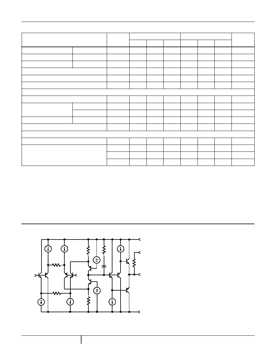
Schematic Diagram
Die Characteristics
Thermal Constants (
o
C/W)
JA
JC
HFA1-0001-5/-9
75
13
HFA3-0001-5
98
36
HFA9P-0001-5/-9
96
27
V+
+IN
R
SENSE
V
OUT
-IN
V-
HFA-0001
4
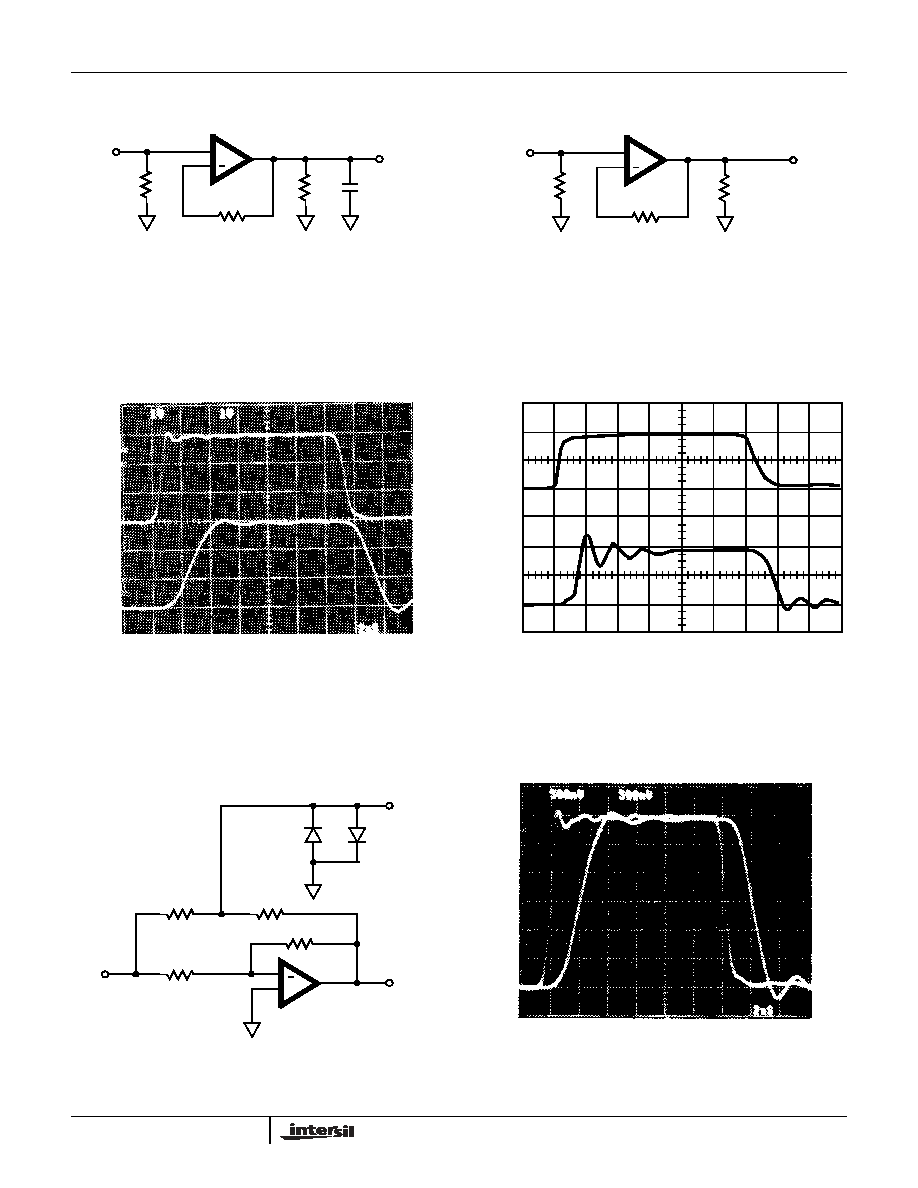
Test Circuits
FIGURE 1. LARGE SIGNAL RESPONSE TEST CIRCUIT
FIGURE 2. SMALL SIGNAL RESPONSE TEST CIRCUIT
LARGE SIGNAL RESPONSE
V
OUT
= 0V to 3V
Vertical Scale: 1V/Div.
Horizontal Scale: 2ns/Div.
SMALL SIGNAL RESPONSE
V
OUT
= 0mV to 200mV
Vertical Scale: 100mV/Div.
Horizontal Scale: 2ns/Div.
NOTE: Initial Step In Output Is Due To Fixture Feedthrough
FIGURE 3. SETTLING TIME SCHEMATIC
PROPAGATION DELAY
Vertical Scale: 500mV/Div.
Horizontal Scale: 2ns/Div.
A
V
= +1, R
L
= 100
, V
OUT
= 0V to 3V
NOTE: Test Fixture Delay of 450ps is Included
V
IN
V
OUT
+
1k
50
20pF
50
V
IN
V
OUT
+
100
50
50
V
IN
V
OUT
V
IN
V
OUT
V
IN
+
1k
V
SETTLE
V
OUT
1k
100
100
HFA-0001
5
Typical Performance Curves
V
S
=
±
5V, T
A
= +25
o
C, Unless Otherwise Specified
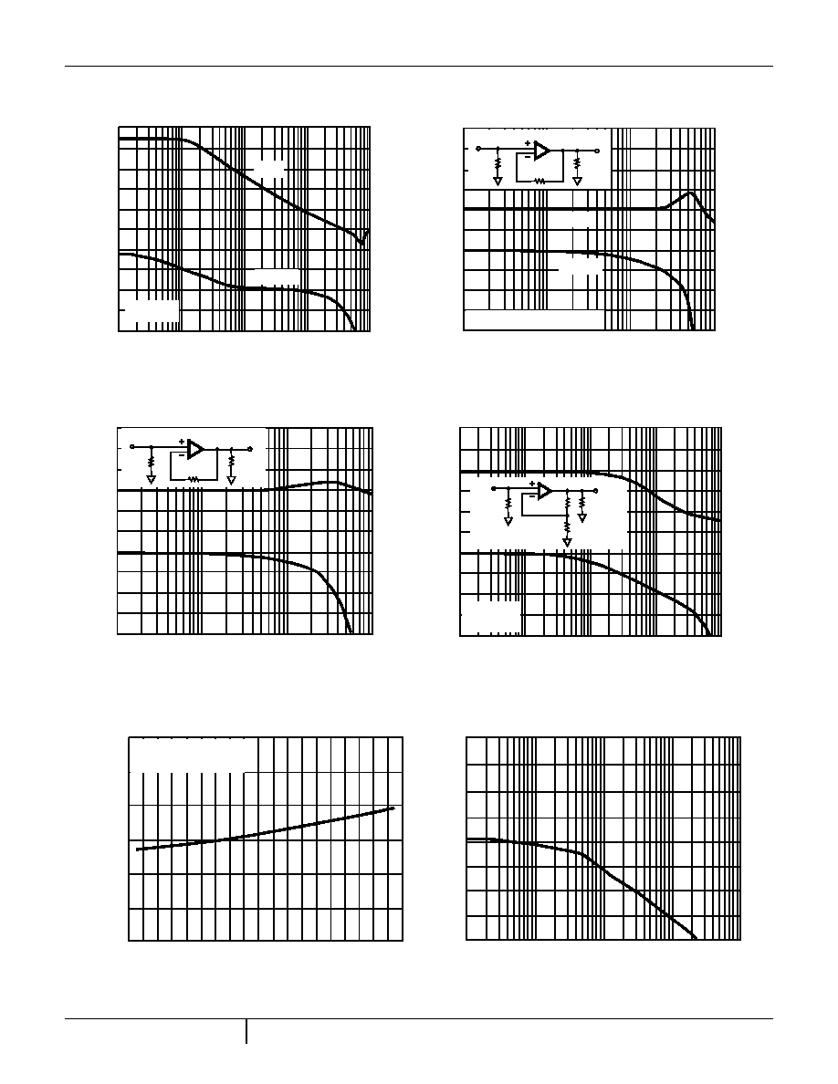
FIGURE 4. OPEN LOOP GAIN AND PHASE vs FREQUENCY
FIGURE 5. CLOSED LOOP GAIN vs FREQUENCY
FIGURE 6. CLOSED LOOP GAIN vs FREQUENCY
FIGURE 7. CLOSED LOOP GAIN vs FREQUENCY
FIGURE 8. RISE TIME vs TEMPERATURE
FIGURE 9. CMRR vs FREQUENCY
G
A
IN (
d
B)
50
40
30
20
10
0
100K
1M
10M
100M
FREQUENCY (Hz)
1G
0
45
90
135
180
P
HAS
E
M
ARG
IN (
D
E
G
RE
E
S
)
GAIN
PHASE
R
L
= 100
10M
100M
1G
1M
FREQUENCY (Hz)
G
A
IN (
d
B)
0
-10
-20
0
45
90
135
180
P
HAS
E
M
ARG
IN
(
D
E
G
RE
E
S
)
20
10
GAIN
PHASE
V
IN
50
100
V
OUT
50
A
V
= +1, R
L
= 100
, R
F
= 50
10M
100M
1G
1M
FREQUENCY (Hz)
G
A
IN (
d
B)
P
HAS
E
M
ARG
IN (
D
E
G
RE
E
S
)
0
45
90
135
180
20
10
0
-10
-20
V
IN
50
100
V
OUT
100
100K
1M
10M
100M
FREQUENCY (Hz)
1G
G
A
IN (
d
B)
P
HAS
E
M
ARG
IN (
D
E
G
RE
E
S
)
0
45
90
135
180
30
20
10
0
-10
V
IN
V
OUT
900
100
100
50
A
V
= +10
R
L
= 100
700
600
500
400
300
200
100
RIS
E
T
I
M
E
(
p
s
)
-60
-40
-20
0
20
40
60
80
100
120
TEMPERATURE (
o
C)
A
V
= +1, R
L
= 100
V
OUT
= 0mV to 200mV
100K
1M
10M
100M
FREQUENCY (Hz)
1G
CM
RR (
d
B)
50
40
30
20
10
0
60
70
80
HFA-0001
Document Outline