 | ÐлекÑÑоннÑй компоненÑ: HFA1103 | СкаÑаÑÑ:  PDF PDF  ZIP ZIP |
Äîêóìåíòàöèÿ è îïèñàíèÿ www.docs.chipfind.ru
1
File Number
3957.3
CAUTION: These devices are sensitive to electrostatic discharge; follow proper IC Handling Procedures.
1-888-INTERSIL or 321-724-7143
|
Copyright
©
Intersil Corporation 1999
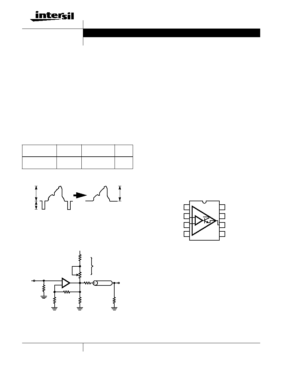
HFA1103
200MHz, Video Op Amp with High Speed
Sync Stripper
The HFA1103 is a high-speed, wideband, fast settling
current feedback op amp with a sync stripping function. The
HFA1103 is a basic op amp with a modified output stage that
enables it to strip the sync from a component video signal.
The output stage has an open emitter NPN transistor that
prevents the output from going low during the sync pulse.
Removing the sync signal benefits digitizing systems
because only the active video information is applied to the
A/D converter. This enables the full dynamic range of the
A/D converter to be used to process the video signal. The
HFA1103 includes inverting input bias current adjust pins
(pins 1 and 5) for adjusting the output offset voltage.
Sync Stripper Waveforms
Application Schematic
Features
· Removes Sync Signal From Component Video
· Low Residual Sync . . . . . . . . . . . . . . . . . . . . . . 8mV (Typ)
· -3dB Bandwidth . . . . . . . . . . . . . . . . . . . . . . . . . . 200MHz
· Very Fast Slew Rate . . . . . . . . . . . . . . . . . . . . . . . 600V/
µ
s
· Fast Settling Time (0.1%) . . . . . . . . . . . . . . . . . . . . . . 9ns
· Excellent Gain Flatness, 32MHz . . . . . . . . . . . . . .
±
0.1dB
· Overdrive Recovery . . . . . . . . . . . . . . . . . . . . . . . . <12ns
Applications
· RGB Video Sync Stripping
· RGB Video Distribution Amplifier for Workstations and PC
Networks
· Video Conferencing Systems
· RGB Video Monitor Preamp
· Fiberoptic Receivers
Pinout
HFA1103
(SOIC)
TOP VIEW
Ordering Information
PART NUMBER
(BRAND)
TEMP.
RANGE (
o
C)
PACKAGE
PKG.
NO.
HFA1103IB
(H1103I)
-40 to 85
8 Ld SOIC
M8.15
0 TO
0 TO
0 TO
+0.7V
-0.3V
+0.7V
COMPONENT (RGB)
VIDEO INPUT
HFA1103 OUTPUT
+5V
HFA1103
R
IN
75
R
F
4.7K
R
L
75
750
R
G
750
V
OUT
V
IN
R
B
R
T
R
T
75
75
2K
+
-
BAL
-IN
+IN
V-
1
2
3
4
8
7
6
5
NC
V+
OUT
BAL
-
+
V+
Data Sheet
March 1999

2
Absolute Maximum Ratings
Thermal Information
Voltage Between V+ and V- . . . . . . . . . . . . . . . . . . . . . . . . . . . . .12V
Input Voltage . . . . . . . . . . . . . . . . . . . . . . . . . . . . . . . . . . . V
SUPPLY
Differential Input Voltage . . . . . . . . . . . . . . . . . . . . . . . . . . . . . . . .5V
Output Current (50% Duty Cycle) . . . . . . . . . . . . . . . . . . . . . . 60mA
Operating Conditions
Temperature Range . . . . . . . . . . . . . . . . . . . . . . . . . . -40
o
C to 85
o
C
Thermal Resistance (Typical, Note 1)
JA
(
o
C/W)
SOIC Package . . . . . . . . . . . . . . . . . . . . . . . . . . . . .
170
Maximum Junction Temperature (Plastic Package) . . . . . . . .150
o
C
Maximum Storage Temperature Range . . . . . . . . . . -65
o
C to 150
o
C
Maximum Lead Temperature (Soldering 10s) . . . . . . . . . . . . .300
o
C
(SOIC - Lead Tips Only)
CAUTION: Stresses above those listed in "Absolute Maximum Ratings" may cause permanent damage to the device. This is a stress only rating and operation of the
device at these or any other conditions above those indicated in the operational sections of this specification is not implied.
NOTE:
1.
JA
is measured with the component mounted on an evaluation PC board in free air.
Electrical Specifications
V
SUPPLY
=
±
5V, A
V
= +2, R
F
= 750
, R
L
= 50
, Unless Otherwise Specified
PARAMETER
TEST CONDITIONS
TEMP
(
o
C)
MIN
TYP
MAX
UNITS
DC CHARACTERISTICS
Residual Sync (Note 2)
V
IN
= -300mV, A
V
= +1
25
-
8
10
mV
Full
-
-
12
mV
Output Offset Voltage (Notes 3, 5)
25
-
10
30
mV
Full
-
-
40
mV
Output Offset Voltage Drift (Note 3)
Full
-
10
-
µ
V/
o
C
V
OS
PSRR
V
S
=
±
1.25V
25
39
45
-
dB
Full
35
-
-
dB
Non-Inverting Input Bias Current
+IN = 0V
25
-
5
40
µ
A
Full
-
-
65
µ
A
Inverting Input Bias Current
-IN = 0V
25
-
5
50
µ
A
Full
-
-
60
µ
A
-I
BIAS
Adjust Range (Notes 4, 6)
25
100
200
-
µ
A
Non-Inverting Input Resistance
25
25
50
-
k
Inverting Input Resistance
25
-
16
30
Input Capacitance
25
-
2
-
pF
Input Common Mode Range
Full
±
2.5
±
3.0
-
V
Input Noise Voltage
100kHz
25
-
4
-
nV/
Hz
+Input Noise Current
100kHz
25
-
18
-
pA/
Hz
-Input Noise Current
100kHz
25
-
21
-
pA/
Hz
TRANSFER CHARACTERISTICS A
V
= +2, Unless Otherwise Specified
Open Loop Transimpedance
25
-
500
-
k
-3dB Bandwidth
V
OUT
= 1.0V
P-P
, A
V
= +2
25
-
200
-
MHz
Gain Flatness
To
±
0.1dB
25
-
32
-
MHz
Minimum Stable Gain
Full
1
-
-
V/V
OUTPUT CHARACTERISTICS A
V
= +2, Unless Otherwise Specified
Output Voltage (Note 3)
25, 85
2.5
3.0
-
V
-40
o
C
1.75
2.5
-
V
Output Current
25, 85
50
60
-
mA
-40
o
C
35
50
-
mA
Linearity Near Zero
25
-
0.01
-
%
TRANSIENT RESPONSE
A
V
= +2, Unless Otherwise Specified
Rise Time
V
OUT
= 2.0V Step
25
-
2
-
ns
HFA1103
3
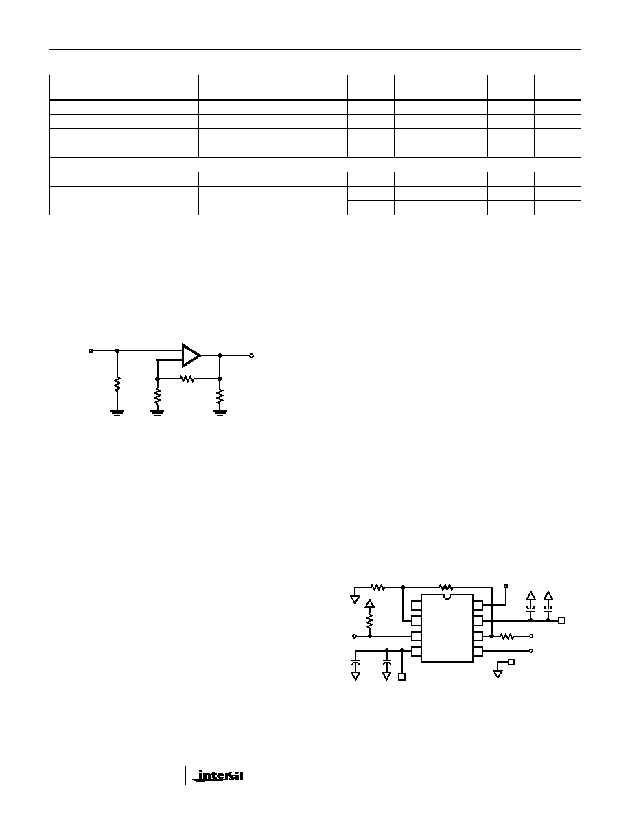
Test Circuit
Application Information
Offset Adjustment
The HFA1103 allows for adjustment of the inverting input bias
current to null the output offset voltage. -I
BIAS
flows through
R
F
, so any change in bias current forces a corresponding
change in output voltage. The amount of adjustment is a
function of R
F
. With R
F
= 750
, the typical adjust range is
150mV. For offset adjustment connect a 10k
potentiometer
between pins 1 and 5 with the wiper connected to V-.
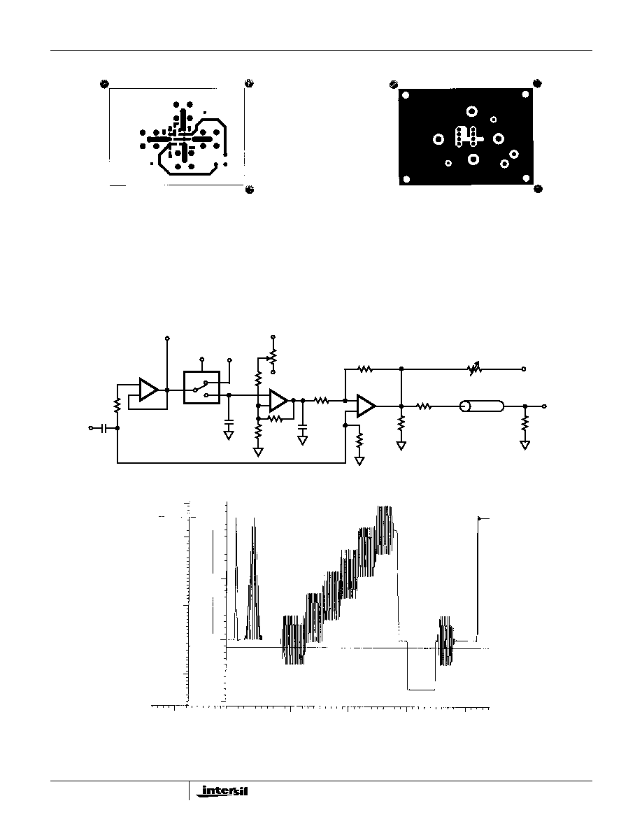
PC Board Layout
The frequency performance of these amplifiers depends a
great deal on the amount of care taken in designing the PC
board. The use of low inductance components such as
chip resistors and chip capacitors is strongly
recommended, while a solid ground plane is a must!
Attention should be given to decoupling the power supplies.
A large value (10
µ
F) tantalum in parallel with a small value
chip (0.1
µ
F) capacitor works well in most cases.
Terminated microstrip signal lines are recommended at the
input and output of the device. Output capacitance, such as
that resulting from an improperly terminated transmission
line will degrade the frequency response of the amplifier and
may cause oscillations. In most cases, the oscillation can be
avoided by placing a resistor in series with the output.
Care must also be taken to minimize the capacitance to
ground seen by the amplifier's inverting input. The larger this
capacitance, the worse the gain peaking, resulting in pulse
overshoot and possible instability. To this end, it is
recommended that the ground plane be removed under
traces connected to pin 2, and connections to pin 2 should
be kept as short as possible.
An example of a good high frequency layout is the
Evaluation Board shown in Figure 3.
Evaluation Board
The HFA1100 series evaluation board may be used for the
HFA1103 with minor modifications. The evaluation board
may be ordered using part number HFA11XXEVAL. Please
note that an HFA1103 sample is not included with the
evaluation board and must be ordered separately.
The layout and schematic of the board are shown below:
Overshoot
V
OUT
= 2.0V Step
25
-
10
-
%
Slew Rate
A
V
= +2, V
OUT
= 0 to 2V, +2V to 0V
25
-
600
-
V/
µ
s
0.1% Settling
V
OUT
= 2V to 0V
25
-
9
-
ns
Overdrive Recovery Time
2X Overdrive
25
-
12
-
ns
POWER SUPPLY CHARACTERISTICS
Supply Voltage Range
Full
±
4.5
-
±
5.5
V
Supply Current (No Load)
25
-
11
16
mA
Full
-
-
23
mA
NOTES:
2. The residual sync is specified at the output of a doubly terminated circuit (see page 1 of this data sheet).
3. Since the HFA1103 has an open emitter NPN output stage, this measurement is only valid for positive values.
4. The -I
BIAS
current can be used to adjust the offset voltage to zero, but -I
BIAS
does not flow bidirectionally because the HFA1103 output stage
is an open emitter NPN transistor.
5. V
OS
includes the error contribution of I
BSN
at R
F
= 750
.
6. This is the minimum change in inverting input bias current when a BAL pin is connected to V- through a 50
resistor.
Electrical Specifications
V
SUPPLY
=
±
5V, A
V
= +2, R
F
= 750
, R
L
= 50
, Unless Otherwise Specified (Continued)
PARAMETER
TEST CONDITIONS
TEMP
(
o
C)
MIN
TYP
MAX
UNITS
V
OUT
R
IN
V
IN
DUT
50
R
G
750
R
F
750
R
L
50
+
-
FIGURE 1. TEST CIRCUIT
1
2
3
4
8
7
6
5
+5V
10
µ
F
0.1
µ
F
V
H
50
GND
GND
500
500
-5V
0.1
µ
F
10
µ
F
50
IN
OUT
V
L
FIGURE 2. EVALUATION BOARD SCHEMATIC
HFA1103
4
Typical Application
A circuit which performs the sync stripper and DC restore
functions is shown in Figure 4. Please reference Intersil
Application Note AN9514, titled "Video Amplifier with Sync
Stripper and DC Restore", for details on this circuit.
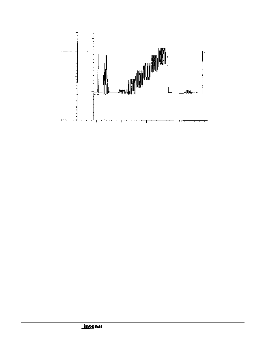
The standard output of a VM700 video measurement set is
shown in Figure 5. The output, after passing through the
Applications Schematic shown on the first page of this data
sheet, is shown in Figure 6.
V
H
+IN
V
L
V+
GND
1
V-
OUT
TOP LAYOUT
BOTTOM LAYOUT
FIGURE 3. EVALUATION BOARD ARTWORK
FIGURE 4. VIDEO AMPLIFIER WITH SYNC STRIPPER AND DC RESTORE
FIGURE 5. OUTPUT OF VM700 VIDEO MEASUREMENT SET
V
OUT
V
IN
-5V
R
7
750
+
-
+
-
+5V
10K
R
3
10K
R
2
S/H
CONTROL
IC2
C
1
0.1
µ
F
1K
R
4
1K
R
5
C
2
47
µ
F
750
R
6
IC1a
TO SYNC
SEPARATOR
1K
R
1
OPT.
IC1b
-
+
10K
R
9
IC3
75
+5V
DC
R
8
6.8K
R
11
75
75
R
10
IC1a + IC1b = CA5260 DUAL AMP
IC2 = 74HC4053 SWITCH
IC3 = HFA1103 VIDEO OP AMP
R
12
0.6
0.4
0.2
0.0
-0.2
VOLTS
IRE:FLT
100.0
50.0
0.0
-50.0
-40.0
-30.0
-20.0
-10.0
0.0
10.0
525 LINE NTSC
MICROSECONDS
HFA1103
5
FIGURE 6. OUTPUT OF HFA1103 SYNC STRIPPER CONFIGURED AS ON THE FIRST PAGE OF THIS DATA SHEET
0.6
0.4
0.2
0.0
-0.2
VOLTS
100.0
50.0
0.0
-50.0
IRE:FLT
-40.0
-30.0
-20.0
-10.0
0.0
10.0
525 LINE NTSC
MICROSECONDS
HFA1103