194
TM
HFA1115/883
High Speed, Low Power, Output Limiting
Closed Loop Buffer Amplifier
Description
The HFA1115/883 is a high speed closed loop Buffer featur-
ing both user programmable gain and output limiting. Manu-
factured in Intersil' proprietary complementary bipolar UHF-1
process, the HFA1115/883 also offers a wide -3dB band-
width of 225MHz, very fast slew rate, excellent gain flatness
and high output current.
This buffer is the ideal choice for high frequency applications
requiring output limiting, especially those needing ultra fast
overload recovery times. The limiting function allows the
designer to set the maximum positive and negative output lev-
els, thereby protecting later stages from damage or input satu-
ration. The HFA1115/883 also allows for voltage gains of +2,
+1, and -1, without the use of external resistors. Gain selec-
tion is accomplished via connections to the inputs, as
described in the "Application Information" text. The result is a
more flexible product, fewer part types in inventory, and more
efficient use of board space.
Compatibility with existing op amp pinouts provides flexibility to
upgrade low gain amplifiers, while decreasing component
count. Unlike most buffers, the standard pinout provides an
upgrade path should a higher closed loop gain be needed at a
future date.
Ordering Information
PART NUMBER
TEMPERATURE
RANGE
PACKAGE
HFA1115MJ/883
-55
o
C to +125
o
C
8 Lead CerDIP
Features
∑ This Circuit is Processed in Accordance to MIL-STD-
883 and is Fully Conformant Under the Provisions of
Paragraph 1.2.1.
∑ User Programmable Output Voltage Limiting
∑ User Programmable For Closed-Loop Gains of +1, -1
or +2 Without Use of External Resistors
∑ Standard Operational Amplifier Pinout
∑ Fast Overdrive Recovery . . . . . . . . . . . . . . . <1ns (Typ)
∑ Low Supply Current. . . . . . . . . . . . . . . . . . 6.9mA (Typ)
∑ Excellent Gain Accuracy . . . . . . . . . . . . . . 0.99V/V (Typ)
∑ Wide -3dB Bandwidth . . . . . . . . . . . . . . . 225MHz (Typ)
∑ Fast Slew Rate . . . . . . . . . . . . . . . . . . . . 1135V/
µs (Typ)
∑ High Input Impedance . . . . . . . . . . . . . . . . . . 1M
(Typ)
∑ Excellent Gain Flatness (to 50MHz) . . . . .
±0.1dB (Typ)
Applications
∑ Flash A/D Driver
∑ Video Switching and Routing
∑ Pulse and Video Amplifiers
∑ Wideband Amplifiers
∑ RF/IF Signal Processing
∑ Medical Imaging Systems
July 1994
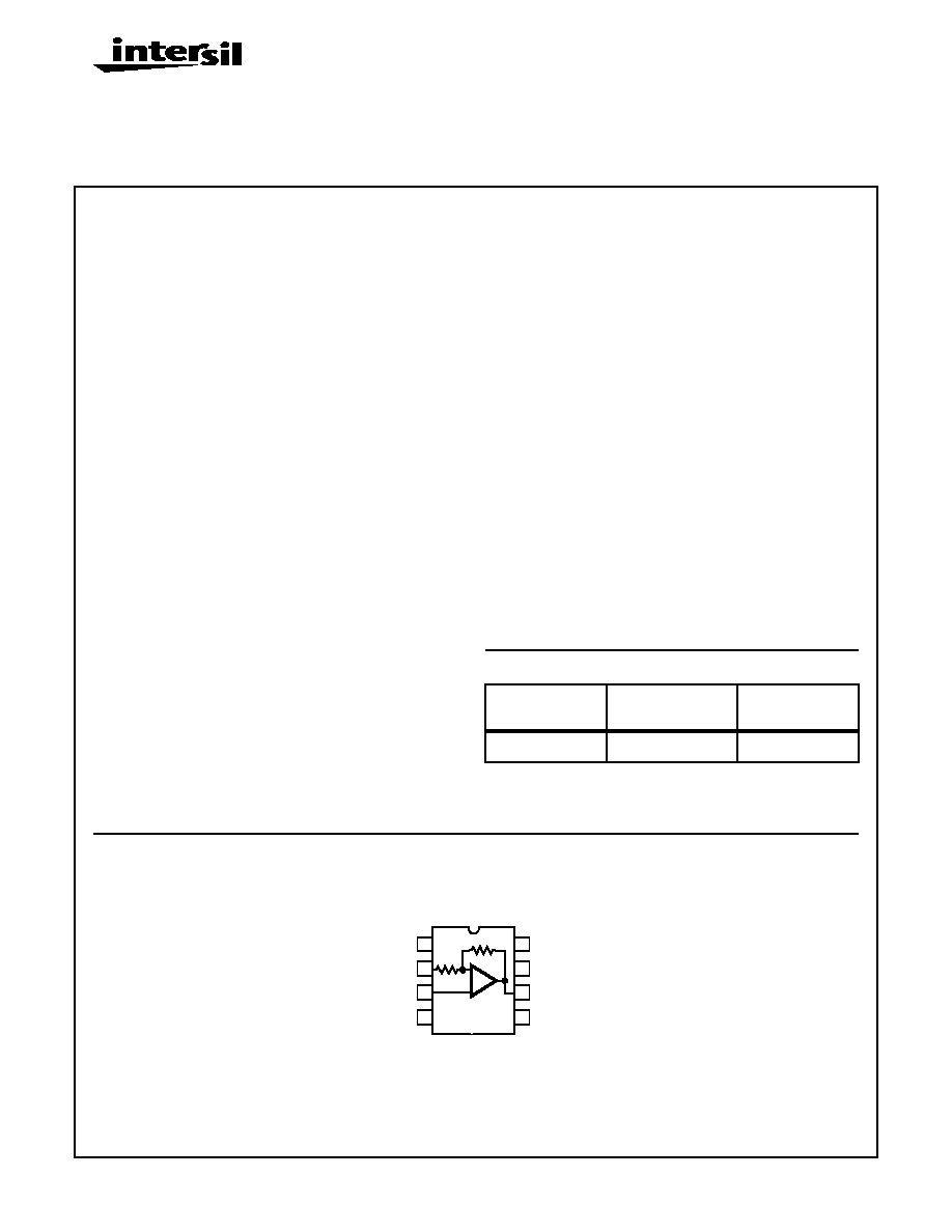
Pinout
HFA1115/883
(CERDIP)
TOP VIEW
NC
-IN
+IN
V-
1
2
3
4
8
7
6
5
V
H
V+
OUT
V
L
350
350
+
-
Spec Number
511109-883
FN3724
CAUTION: These devices are sensitive to electrostatic discharge; follow proper IC Handling Procedures.
1-888-INTERSIL or 321-724-7143
|
Intersil (and design) is a trademark of Intersil Americas Inc.
Copyright © Intersil Americas Inc. 2002. All Rights Reserved
195
Specifications HFA1115/883
Absolute Maximum Ratings
Thermal Information
Voltage Between V+ and V- . . . . . . . . . . . . . . . . . . . . . . . . . . . . 12V
Voltage at Either Input Terminal. . . . . . . . . . . . . . . . . . . . . . V+ to V-
Output Current (Note 1) . . . . . . . . . . . . . . . . Short Circuit Protected
Output Current (50% Duty Cycle, Note 1) . . . . . . . . . . . . . . . . 60mA
Junction Temperature. . . . . . . . . . . . . . . . . . . . . . . . . . . . . . +175
o
C
ESD Rating. . . . . . . . . . . . . . . . . . . . . . . . . . . . . . . . . . . . . . > 2000V
Storage Temperature Range . . . . . . . . . . . . . . -65
o
C
T
A
+150
o
C
Lead Temperature (Soldering 10s). . . . . . . . . . . . . . . . . . . . +300
o
C
Thermal Resistance
JA
JC
CerDIP Package . . . . . . . . . . . . . . . . . 115
o
C/W
30
o
C/W
Maximum Package Power Dissipation at +75
o
C
CerDIP Package . . . . . . . . . . . . . . . . . . . . . . . . . . . . . . . . . 0.87W
Package Power Dissipation Derating Factor above +75
o
C
CerDIP Package . . . . . . . . . . . . . . . . . . . . . . . . . . . . . . 8.7mW/
o
C
CAUTION: Stresses above those listed in "Absolute Maximum Ratings" may cause permanent damage to the device. This is a stress only rating and operation
of the device at these or any other conditions above those indicated in the operational sections of this specification is not implied.
Operating Conditions
Operating V
SUPPLY
(
±V
S
)
. . . . . . . . . . . . . . . . . . . . . . . . . . . . . . . . . ±5V
Operating Temperature Range. . . . . . . . . . . . .-55
o
C
T
A
+125
o
C
R
L
S
50
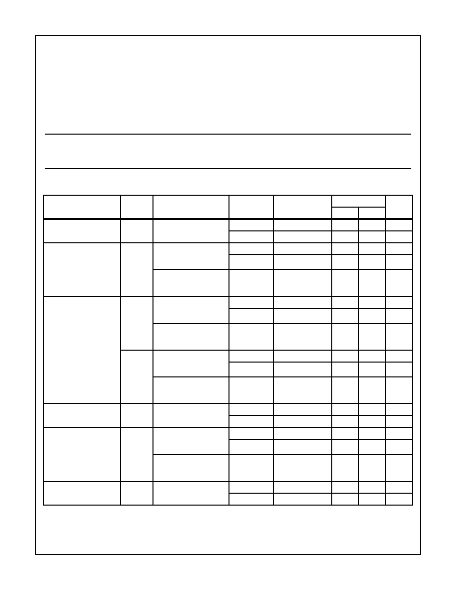
TABLE 1. DC ELECTRICAL PERFORMANCE CHARACTERISTICS
Device Tested at: V
SUPPLY
=
±5V, A
V
= +1, R
SOURCE
= 0
, R
L
= 100
, V
OUT
= 0V, Unless Otherwise Specified.
PARAMETERS
SYMBOL
CONDITIONS
GROUP A
SUBGROUPS
TEMPERATURE
LIMITS
UNITS
MIN
MAX
Output Offset Voltage
V
OS
V
CM
= 0V
1
+25
o
C
-10
10
mV
2, 3
+125
o
C, -55
o
C
-20
20
mV
Common Mode
Rejection Ratio
CMRR
V
CM
=
±1.8V
V+ = 3.2V, V- = -6.8V
V+ = 6.8V, V- = -3.2V
1
+25
o
C
42
-
dB
2
+125
o
C
39
-
dB
V
CM
=
±1.2V
V+ = 3.8V, V- = -6.2V
V+ = 6.2V, V- = -3.8V
3
-55
o
C
39
-
dB
Power Supply
Rejection Ratio
PSRRP
V
SUPPLY
=
±1.8V
V+ = 6.8V, V- = -5V
V+ = 3.2V, V- = -5V
1
+25
o
C
45
-
dB
2
+125
o
C
42
-
dB
V
SUPPLY
=
±1.2V
V+ = 6.2V, V- = -5V
V+ = 3.8V, V- = -5V
3
-55
o
C
42
-
dB
PSRRN
V
SUPPLY
=
±1.8V
V+ = 5V, V- = -6.8V
V+ = 5V, V- = -3.2V
1
+25
o
C
45
-
dB
2
+125
o
C
42
-
dB
V
SUPPLY
=
±1.2V
V+ = 5V, V- = -6.2V
V+ = 5V, V- = -3.8V
3
-55
o
C
42
-
dB
Non-Inverting Input (+IN)
Current
I
BSP
V
CM
= 0V
1
+25
o
C
-15
15
µA
2, 3
+125
o
C, -55
o
C
-25
25
µA
+IN Current Common
Mode Sensitivity
CMS
IBP
V
CM
=
±1.8V
V+ = 3.2V, V- = -6.8V
V+ = 6.8V, V- = -3.2V
1
+25
o
C
-
1.25
µA/V
2
+125
o
C
-
2.85
µA/V
V
CM
=
±1.2V
V+ = 3.8V, V- = -6.2V
V+ = 6.2V, V- = -3.8V
3
-55
o
C
-
2.85
µA/V
+IN Resistance
+R
IN
Note 2
1
+25
o
C
800
-
k
2, 3
+125
o
C, -55
o
C
350
-
k
Spec Number
511109-883

196
Specifications HFA1115/883
Gain
A
VP1
A
V
= +1
V
IN
= -1V to +1V
1
+25
o
C
0.98
1.02
V/V
2, 3
+125
o
C, -55
o
C
0.975
1.025
V/V
A
VM1
A
V
= -1
V
IN
= -1V to +1V
1
+25
o
C
-0.98
-1.02
V/V
2, 3
+125
o
C, -55
o
C
-0.975
-1.025
V/V
A
VP2
A
V
= +2
V
IN
= -1V to +1V
1
+25
o
C
1.96
2.04
V/V
2, 3
+125
o
C, -55
o
C
1.95
2.05
V/V
Output Voltage Swing
V
OP100
A
V
= -1
R
L
= 100
V
IN
= -3.2V
1
+25
o
C
3
-
V
V
IN
= -3V
2, 3
+125
o
C, -55
o
C
2.8
-
V
V
ON100
A
V
= -1
R
L
= 100
V
IN
=+3.2V
1
+25
o
C
-
-3
V
V
IN
= +3V
2, 3
+125
o
C, -55
o
C
-
-2.8
V
Output Voltage Swing
V
OP50
A
V
= -1
R
L
= 50
V
IN
= -2.7V
1
+25
o
C
2.5
-
V
V
IN
= -2.25V
2
+125
o
C
2.0
-
V
V
IN
= -2.25V
3
-55
o
C
1.4
-
V
V
ON50
A
V
= -1
R
L
= 50
V
IN
= +2.7V
1
+25
o
C
-
-2.5
V
V
IN
= +2.25
V
2
+125
o
C
-
-2.0
V
V
IN
= +2.25
V
3
-55
o
C
-
-1.4
V
Output Current
+I
OUT
Note 3
1
+25
o
C
50
-
mA
2
+125
o
C
40
-
mA
3
-55
o
C
28
-
mA
-I
OUT
Note 3
1
+25
o
C
-
-50
mA
2
+125
o
C
-
-40
mA
3
-55
o
C
-
-28
mA
Quiescent Power
Supply Current
I
CC
R
L
= 100
1
+25
o
C
6.6
7.1
mA
2, 3
+125
o
C, -55
o
C
6.2
7.5
mA
I
EE
R
L
= 100
1
+25
o
C
-7.1
-6.6
mA
2, 3
+125
o
C, -55
o
C
-7.5
-6.2
mA
Clamp Accuracy
V
H
CLMP
A
V
= -1, V
IN
= -1.6V
V
H
= 1V
1
+25
o
C
-125
125
mV
2, 3
+125
o
C, -55
o
C
-125
125
mV
V
L
CLMP
A
V
= -1, V
IN
= +1.6V
V
L
= -1V
1
+25
o
C
-125
125
mV
2, 3
+125
o
C, -55
o
C
-125
125
mV
Clamp Input Current
V
H
BIAS
V
H
= 1V
1
+25
o
C
-
200
µA
2, 3
+125
o
C, -55
o
C
-
200
µA
V
L
BIAS
V
L
= -1V
1
+25
o
C
-200
-
µA
2, 3
+125
o
C, -55
o
C
-200
-
µA
TABLE 1. DC ELECTRICAL PERFORMANCE CHARACTERISTICS
(Continued)
Device Tested at: V
SUPPLY
=
±5V, A
V
= +1, R
SOURCE
= 0
, R
L
= 100
, V
OUT
= 0V, Unless Otherwise Specified.
PARAMETERS
SYMBOL
CONDITIONS
GROUP A
SUBGROUPS
TEMPERATURE
LIMITS
UNITS
MIN
MAX
Spec Number
511109-883

197
Specifications HFA1115/883
NOTES:
1. Output is short circuit protected to ground. Brief short circuits to ground will not degrade reliability, however continuous (100% duty cycle)
output current must not exceed 30mA for maximum reliability.
2. Guaranteed from +IN Common Mode Rejection Test, by: +R
IN
= 1/CMS
IBP
.
3. Guaranteed from V
OUT
Test with R
L
= 50
, by: I
OUT
= V
OUT
/50
.
TABLE 2. AC ELECTRICAL PERFORMANCE CHARACTERISTICS
Table 2 Intentionally Left Blank.
TABLE 3. ELECTRICAL PERFORMANCE CHARACTERISTICS
Table 3 Intentionally Left Blank.
TABLE 4. ELECTRICAL TEST REQUIREMENTS
MIL-STD-883 TEST REQUIREMENTS
SUBGROUPS (SEE TABLE 1)
Interim Electrical Parameters (Pre Burn-In)
1
Final Electrical Test Parameters
1 (Note 1), 2, 3
Group A Test Requirements
1, 2, 3
Groups C and D Endpoints
1
NOTE:
1. PDA applies to Subgroup 1 only.
TABLE 1. DC ELECTRICAL PERFORMANCE CHARACTERISTICS
(Continued)
Device Tested at: V
SUPPLY
=
±5V, A
V
= +1, R
SOURCE
= 0
, R
L
= 100
, V
OUT
= 0V, Unless Otherwise Specified.
PARAMETERS
SYMBOL
CONDITIONS
GROUP A
SUBGROUPS
TEMPERATURE
LIMITS
UNITS
MIN
MAX
Spec Number
511109-883
198
HFA1115/883
Spec Number
511109-883
Die Characteristics
DIE DIMENSIONS:
59 x 58.2 x 19 mils
± 1 mils
1500 x 1480 x 483
µm ± 25.4µm
METALLIZATION:
Type: Metal 1: AICu(2%)/TiW
Type: Metal 2: AICu(2%)
Thickness: Metal 1: 8k
≈
± 0.4k
≈
Thickness: Metal 2: 16k
≈
± 0.8k
≈
GLASSIVATION:
Type: Nitride
Thickness: 4k
≈
± 0.5k
≈
WORST CASE CURRENT DENSITY:
TBD
TRANSISTOR COUNT: 89
SUBSTRATE POTENTIAL (Powered Up): Floating (Recommend Connection to V-)
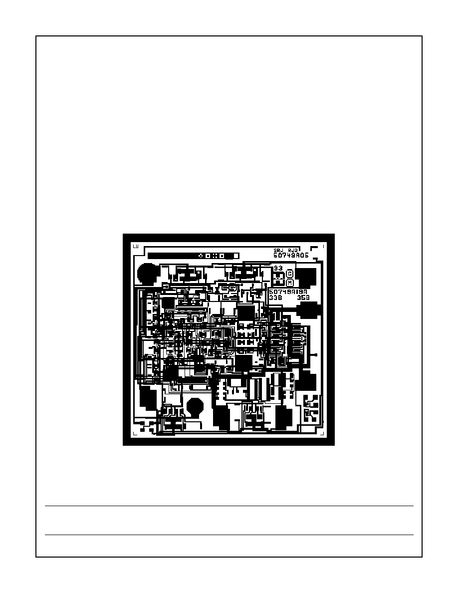
Metallization Mask Layout
HFA1115/883
V-
OUT
+IN
-IN
V+
V
L
V
H
V-
V
L
All Intersil semiconductor products are manufactured, assembled and tested under ISO9000 quality systems certification.
Intersil products are sold by description only. Intersil Corporation reserves the right to make changes in circuit design and/or specifications at any time without notice.
Accordingly, the reader is cautioned to verify that data sheets are current before placing orders. Information furnished by Intersil is believed to be accurate and reli-
able. However, no responsibility is assumed by Intersil or its subsidiaries for its use; nor for any infringements of patents or other rights of third parties which may
result from its use. No license is granted by implication or otherwise under any patent or patent rights of Intersil or its subsidiaries.
For information regarding Intersil Corporation and its products, see web site http://www.intersil.com