 | –≠–ª–µ–∫—Ç—Ä–æ–Ω–Ω—ã–π –∫–æ–º–ø–æ–Ω–µ–Ω—Ç: HFA1149 | –°–∫–∞—á–∞—Ç—å:  PDF PDF  ZIP ZIP |

1
TM
File Number
4304.3
CAUTION: These devices are sensitive to electrostatic discharge; follow proper IC Handling Procedures.
1-888-INTERSIL or 321-724-7143
|
Intersil and Design is a trademark of Intersil Corporation.
|
Copyright
©
Intersil Corporation 2000
HFA1149
450MHz, Low Power, Video Operational
Amplifier with Programmable Output
Disable
The HFA1149 is a high speed, low power, current feedback
amplifier built with Intersil's proprietary complementary
bipolar UHF-1 process. This amplifier features a unique
combination of power and performance specifically tailored
for video applications.
The HFA1149 incorporates an output disable pin which is
TTL/CMOS compatible, and user programmable for polarity
(active high or low). This feature eliminates the inverter
required between amplifiers in multiplexer configurations.
The ultra-fast (12ns/20ns) disable/enable times make the
HFA1149 the obvious choice for pixel switching and other
high speed multiplexing applications. The HFA1149 is a high
performance, pin compatible upgrade for the popular HA-5020
and HFA1145, as well as the CLC410.
For a comparably performing op amp without an output
disable, please refer to the HFA1109 data sheet.
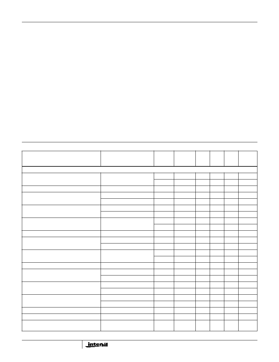
Pinout
HFA1149
(SOIC)
TOP VIEW
Features
∑ Wide - 3dB Bandwidth (A
V
= +2) . . . . . . . . . . . . . 450MHz
∑ Gain Flatness (To 250MHz) . . . . . . . . . . . . . . . . . . . 0.8dB
∑ Very Fast Slew Rate (A
V
= +2) . . . . . . . . . . . . . . 1100V/
µ
s
∑ High Input Impedance . . . . . . . . . . . . . . . . . . . . . . 1.7M
∑ Differential Gain/Phase. . . . . . . . . . . 0.02%/0.02 Degrees
∑ Low Supply Current . . . . . . . . . . . . . . . . . . . . . . . . . 10mA
∑ Fast Output Disable/Enable . . . . . . . . . . . . . . . 12ns/20ns
Applications
∑ Professional Video Processing
∑ Video Switchers and Routers
∑ Medical Imaging
∑ PC Multimedia Systems
∑ Video Pixel Switching
∑ Video Distribution Amplifiers
∑ Flash Converter Drivers
∑ Radar/IF Processing
Ordering Information
PART NUMBER
(BRAND)
TEMP.
RANGE (
o
C)
PACKAGE
PKG.
NO.
HFA1149IB
(H1149)
-40 to 85
8 Ld SOIC
M8.15
HFA11XXEVAL
DIP Evaluation Board for High Speed
Op Amps
THRESHOLD SET
-IN
+IN
V-
1
2
3
4
8
7
6
5
DIS / DIS
V+
OUT
+
-
POLARITY SET
HFA1149 PIN DESCRIPTIONS
PIN NAME
DESCRIPTION
Threshold Set
Optional Logic Threshold Set. Maintains disable
pin TTL compatibility with asymmetrical supplies
(e.g., +10V, 0V).
Polarity Set
Defines Polarity of Disable Input. High or floating
selects active low disable (i.e., DIS).
DIS/DIS
TTL Compatible Disable Input. Output is driven to
a true Hi-Z state when active. Polarity depends on
state of Polarity Set Pin.
HFA1149 DISABLE FUNCTIONALITY
POLARITY SET
(PIN 5)
DISABLE (PIN 8)
OUTPUT (PIN 6)
High or Float
High or Float
Enabled
High or Float
Low
Disabled
Low
High or Float
Disabled
Low
Low
Enabled
Data Sheet
June 2000
2
Absolute Maximum Ratings
Thermal Information
Voltage Between V+ and V- . . . . . . . . . . . . . . . . . . . . . . . . . . . . 12V
DC Analog Input Voltage . . . . . . . . . . . . . . . . . . . . . . . . . . V
SUPPLY
Digital Input Voltage . . . . . . . . . . . . . . . . . . . . . . . . . . V
SUPPLY
±
1V
Differential Input Voltage . . . . . . . . . . . . . . . . . . . . . . . . . . . . . . . 8V
Output Current (Note 2) . . . . . . . . . . . . . . . . Short Circuit Protected
30mA Continuous
60mA
50% Duty Cycle
ESD Rating
Human Body Model (Per MIL-STD-883 Method 3015.7) . . 1000V
Charged Device Model (Per EOS/ESD DS5.3, 4/14/93) . . 1000V
Machine Model (Per EIAJ ED-4701 Method C-111). . . . . . . . 50V
Operating Conditions
Temperature Range . . . . . . . . . . . . . . . . . . . . . . . . . . -40
o
C to 85
o
C
Thermal Resistance (Typical, Note 1)
JA
(
o
C/W)
SOIC Package . . . . . . . . . . . . . . . . . . . . . . . . . . . . .
160
Maximum Junction Temperature (Die) . . . . . . . . . . . . . . . . . . . 175
o
C
Maximum Junction Temperature (Plastic Package) . . . . . . . 150
o
C
Maximum Storage Temperature Range . . . . . . . . . . -65
o
C to 150
o
C
Maximum Lead Temperature (Soldering 10s) . . . . . . . . . . . . 300
o
C
(SOIC - Lead Tips Only)
CAUTION: Stresses above those listed in "Absolute Maximum Ratings" may cause permanent damage to the device. This is a stress only rating and operation of the
device at these or any other conditions above those indicated in the operational sections of this specification is not implied.
NOTES:
1.
JA
is measured with the component mounted on an evaluation PC board in free air.
2. Output is short circuit protected to ground. Brief short circuits to ground will not degrade reliability, however, continuous (100% duty cycle) output
current must not exceed 30mA for maximum reliability.
Electrical Specifications
V
SUPPLY
=
±
5V, A
V
= +2, R
F
= 250
, R
L
= 100
, Unless Otherwise Specified
PARAMETER
TEST CONDITIONS
(NOTE 3)
TEST
LEVEL
TEMP.
(
o
C)
MIN
TYP
MAX
UNITS
INPUT CHARACTERISTICS
Input Offset Voltage
A
25
-
1
5
mV
A
Full
-
2
8
mV
Average Input Offset Voltage Drift
B
Full
-
10
-
µ
V/
o
C
Input Offset Voltage
Common-Mode Rejection Ratio
V
CM
=
±
2V
A
25
47
50
-
dB
V
CM
=
±
2V
A
Full
45
48
-
dB
Input Offset Voltage
Power Supply Rejection Ratio
V
PS
=
±
1.25V
A
25
50
53
-
dB
V
PS
=
±
1.25V
A
Full
47
51
-
dB
Non-Inverting Input Bias Current
A
25
-
4
10
µ
A
A
Full
-
5
15
µ
A
Non-Inverting Input Bias Current Drift
B
Full
-
30
-
nA/
o
C
Non-Inverting Input Bias Current
Power Supply Sensitivity
V
PS
=
±
1.25V
A
25
-
0.5
1
µ
A/V
V
PS
=
±
1.25V
A
Full
-
0.5
3
µ
A/V
Inverting Input Bias Current
A
25
-
2
10
µ
A
A
Full
-
3
15
µ
A
Inverting Input Bias Current Drift
B
Full
-
40
-
nA/
o
C
Inverting Input Bias Current
Common-Mode Sensitivity
V
CM
=
±
2V
A
25
-
3
6
µ
A/V
V
CM
=
±
2V
A
Full
-
3
8
µ
A/V
Inverting Input Bias Current
Power Supply Sensitivity
V
PS
=
±
1.25V
A
25
-
1.6
5
µ
A/V
V
PS
=
±
1.25V
A
Full
-
1.6
8
µ
A/V
Non-Inverting Input Resistance
V
CM
=
±
2V
A
25, 85
0.8
1.7
-
M
V
CM
=
±
2V
A
-40
0.5
1.4
-
M
Inverting Input Resistance
B
25
-
60
-
Input Capacitance
B
25
-
1.6
-
pF
Input Voltage Common Mode Range (Implied
by V
IO
CMRR, +R
IN
, and -I
BIAS
CMS tests)
A
Full
±
2
±
2.5
-
V
HFA1149
3
Input Noise Voltage Density (Note 5)
f = 100kHz
B
25
-
4
-
nV/
Hz
Non-Inverting Input Noise Current Density
(Note 5)
f = 100kHz
B
25
-
2.4
-
pA/
Hz
Inverting Input Noise Current Density
(Note 5)
f = 100kHz
B
25
-
40
-
pA/
Hz
TRANSFER CHARACTERISTICS
Open Loop Transimpedance Gain (Note 5)
B
25
-
500
-
k
Minimum Stable Gain
B
Full
-
1
-
V/V
AC CHARACTERISTICS
-3dB Bandwidth
(V
OUT
= 0.2V
P-P
, Note 5)
A
V
= -1, R
F
= 200
B
25
300
375
-
MHz
B
Full
290
360
-
MHz
A
V
= +1, +R
S
= 700
B
25
280
330
-
MHz
B
Full
260
320
-
MHz
A
V
= +2
B
25
390
450
-
MHz
B
Full
350
410
-
MHz
Gain Peaking
A
V
= +2, V
OUT
= 0.2V
P-P
B
25
-
0
0.2
dB
B
Full
-
0
0.5
dB
Gain Flatness
(A
V
= +2, V
OUT
= 0.2V
P-P
, Note 5)
To 125MHz
B
25
-1.0
-0.45
-
dB
B
Full
-1.1
-0.45
-
dB
To 200MHz
B
25
-1.6
-0.75
-
dB
B
Full
-1.7
-0.75
-
dB
To 250MHz
B
25
-1.9
-0.85
-
dB
B
Full
-2.2
-0.85
-
dB
Gain Flatness
A
V
= +1, +R
S
= 700
, V
OUT
= 0.2V
P-P
(Note 5)
To 125MHz
B
25
±
0.3
±
0.1
-
dB
B
Full
±
0.4
±
0.1
-
dB
To 200MHz
B
25
±
0.8
±
0.35
-
dB
B
Full
±
0.9
±
0.35
-
dB
To 250MHz
B
25
±
1.3
±
0.6
-
dB
B
Full
±
1.4
±
0.6
-
dB
OUTPUT CHARACTERISTICS
Output Voltage Swing, Unloaded
(Note 5)
A
V
= -1, R
L
=
A
25
±
3
±
3.2
-
V
A
Full
±
2.8
±
3
-
V
Output Current
(Note 5)
A
V
= -1, R
L
= 75
A
25, 85
±
33
±
36
-
mA
A
-40
±
30
±
33
-
mA
Output Short Circuit Current
A
V
= -1
B
25
-
120
-
mA
Closed Loop Output Resistance (Note 5)
DC, A
V
= +1, Enabled
B
25
-
0.05
-
Second Harmonic Distortion
(V
OUT
= 2V
P-P
, Note 5)
20MHz
B
25
-
-55
-
dBc
60MHz
B
25
-
-57
-
dBc
Third Harmonic Distortion
(V
OUT
= 2V
P-P
, Note 5)
20MHz
B
25
-
-68
-
dBc
60MHz
B
25
-
-60
-
dBc
Reverse Isolation (S
12
)
30MHz
B
25
-
-65
-
dB
TRANSIENT CHARACTERISTICS
Rise and Fall Times
V
OUT
= 0.5V
P-P
B
25
-
1.1
1.3
ns
B
Full
-
1.1
1.4
ns
Electrical Specifications
V
SUPPLY
=
±
5V, A
V
= +2, R
F
= 250
, R
L
= 100
, Unless Otherwise Specified (Continued)
PARAMETER
TEST CONDITIONS
(NOTE 3)
TEST
LEVEL
TEMP.
(
o
C)
MIN
TYP
MAX
UNITS
HFA1149
4
Overshoot
V
OUT
= 0.5V
P-P
B
25
-
0
2
%
B
Full
-
0.5
5
%
Slew Rate
A
V
= -1, R
F
= 200
V
OUT
= 5V
P-P
B
25
2300
2600
-
V/
µ
s
B
Full
2200
2500
-
V/
µ
s
A
V
= +1, V
OUT
= 4V
P-P
,
+R
S
= 700
B
25
475
550
-
V/
µ
s
B
Full
430
500
-
V/
µ
s
A
V
= +2, V
OUT
= 5V
P-P
B
25
940
1100
-
V/
µ
s
B
Full
800
950
-
V/
µ
s
Settling Time
(V
OUT
= +2V to 0V step, Note 5)
To 0.1%
B
25
-
19
-
ns
To 0.05%
B
25
-
23
-
ns
To 0.01%
B
25
-
36
-
ns
Overdrive Recovery Time
V
IN
=
±
2V
B
25
-
5
-
ns
VIDEO CHARACTERISTICS
Differential Gain
(f = 3.58MHz)
R
L
= 150
B
25
-
0.02
0.06
%
B
Full
-
0.03
0.09
%
R
L
= 75
B
25
-
0.04
0.09
%
B
Full
-
0.05
0.12
%
Differential Phase
(f = 3.58MHz)
R
L
= 150
B
25
-
0.02
0.06
Degrees
B
Full
-
0.02
0.06
Degrees
R
L
= 75
B
25
-
0.05
0.09
Degrees
B
Full
-
0.06
0.13
Degrees
POWER SUPPLY CHARACTERISTICS
Power Supply Range
C
25
±
4.5
-
±
5.5
V
Power Supply Current (Note 4)
A
25
-
9.6
10
mA
A
Full
-
10
11
mA
HFA1149 DISABLE CHARACTERISTICS Polarity Set = Floating, Threshold Set = Floating, Unless Otherwise Specified
Disabled Supply Current
V
DIS
= 0V
A
Full
-
2.8
3.5
mA
Digital Input Logic Low (Note 4)
A
Full
-
-
0.8
V
Digital Input Logic High (Note 4)
A
25
2.0
-
-
V
A
Full
2.2
-
-
V
Digital Input Logic Low Current (Note 4)
V
DIGITAL
= 0V
A
Full
-
100
200
µ
A
Digital Input Logic High Current (Note 4)
V
DIGITAL
= 5V
A
Full
-
1
15
µ
A
Output Disable Time (Note 5)
V
IN
=
±
0.5V,
V
DIS
= 2.4V to 0V
B
25
-
12
-
ns
Output Enable Time (Note 5)
V
IN
=
±
0.5V,
V
DIS
= 0V to 2.4V
B
25
-
20
-
ns
Disabled Output Capacitance
V
DIS
= 0V
B
25
-
2.5
-
pF
Disabled Output Leakage
V
DIS
= 0V, V
IN
=
2V,
V
OUT
=
±
3V
A
Full
-
3
10
µ
A
Off Isolation
(V
DIS
= 0V, V
IN
= 1V
P-P
, Note 5)
At 10MHz
B
25
-
-64
-
dB
At 30MHz
B
25
-
-54
-
dB
NOTES:
3. Test Level: A. Production tested; B. Typical or guaranteed limit based on characterization; C. Design Typical for information only.
4. Digital inputs are Polarity Set and DIS / DIS.
5. See Typical Performance Curves for more information.
Electrical Specifications
V
SUPPLY
=
±
5V, A
V
= +2, R
F
= 250
, R
L
= 100
, Unless Otherwise Specified (Continued)
PARAMETER
TEST CONDITIONS
(NOTE 3)
TEST
LEVEL
TEMP.
(
o
C)
MIN
TYP
MAX
UNITS
±
HFA1149
5
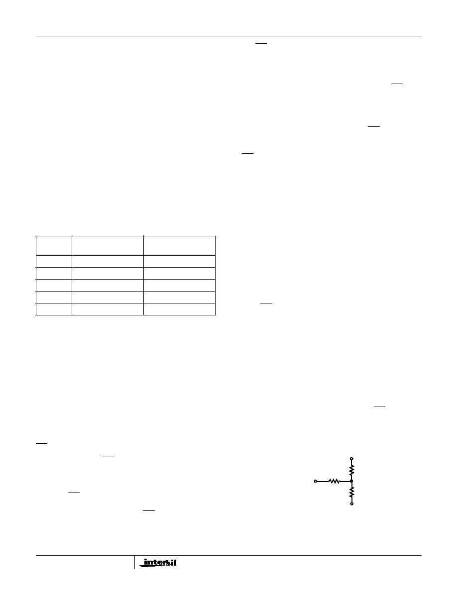
Application Information
Optimum Feedback Resistor
Although a current feedback amplifier's bandwidth
dependency on closed loop gain isn't as severe as that of a
voltage feedback amplifier, there can be an appreciable
decrease in bandwidth at higher gains. This decrease may
be minimized by taking advantage of the current feedback
amplifier's unique relationship between bandwidth and R
F
.
All current feedback amplifiers require a feedback resistor,
even for unity gain applications, and R
F
, in conjunction with
the internal compensation capacitor, sets the dominant pole
of the frequency response. Thus, the amplifier's bandwidth is
inversely proportional to R
F
. The HFA1149 design is
optimized for a 250
R
F
at a gain of +2. Decreasing R
F
decreases stability, resulting in excessive peaking and
overshoot (Note: Capacitive feedback will cause the same
problems due to the feedback impedance decrease at higher
frequencies). At higher gains the amplifier is more stable, so
R
F
can be decreased in a trade-off of stability for bandwidth.
Table 1 lists recommended R
F
values, and the expected
bandwidth, for various closed loop gains. For a gain of +1, a
resistor (
+
R
S
) in series with +IN is required to reduce gain
peaking and increase stability
Output Disable Function
The HFA1149 incorporates an output disable function that is
useful for reducing power dissipation or for multiplexing
signals onto a common analog bus. When disabled, the
inverting input and the output become high impedances
(however, the feedback network for gains other than +1 still
present a load to ground from the output), the supply current
reduces by 68%, and the input to output isolation becomes
greater than 60dB. The amplifier is disabled by driving the
DIS / DIS input to its active state.
The active state of the DIS / DIS input is user programmable
via the HFA1149's Polarity Set input (see next paragraph). If
the Polarity Set input is left floating, or is tied to a logic high
(e.g., V+), then the disable function is activated by a logic
low on the DIS / DIS input (typical of most output disable op
amps). If the Polarity Set input is connected to a logic low
(e.g., GND), then a logic high on the DIS / DIS input disables
the amplifier.
The DIS / DIS input is TTL compatible, and unlike most
competitive devices, the TTL compatibility can be
maintained when the HFA1149 is operated at supplies other
than
±
5V (see the "Threshold Set input" section below).
An internal resistive bias network ensures that the DIS / DIS
pin is pulled high if it is undriven on the PCB.
Polarity Set Input
A novel feature of the HFA1149 is the polarity
programmability of the disable control pin (DIS / DIS).
Depending on the state of the Polarity Set input (pin 5), the
designer can define the active state to be high or low for the
DIS / DIS input (see the "HFA1149 Disable Functionality"
table on the front page). With this feature, a 2:1 multiplexer
can be created by defining one amplifier's disable control as
active low (Polarity Set = High or floating), and the other
amplifier's control as active high (Polarity Set = Low). Note
that if the Polarity Set pin is left floating, an internal pull-up
resistor pulls the pin high, and the HFA1149 becomes a
drop-in replacement for any standard
±
5V supply op amp
with output disable (e.g., CLC410, CLC411, CLC430,
HA-5020, HFA1145, AD810). Likewise, if the disable and
polarity set pins are both floated, the HFA1149 works just
like a standard op amp (i.e., the output is always enabled).
Threshold Set Input for TTL Compatibility
The HFA1149 derives an internal threshold reference for the
digital circuitry as long as the power supplies are nominally
±
5V. This reference is used to ensure the TTL compatibility
of the DIS / DIS and Polarity Set inputs. With symmetrical
±
5V supplies the Threshold Set pin (Pin 1) must be floated to
guarantee TTL compatibility. If asymmetrical supplies (e.g.,
+10V, 0V) are utilized, and TTL compatibility is desired, the
Threshold Set pin must be connected to an external voltage
(e.g., GND for +10V, 0V operation). The following equation
should be used to determine the voltage (V
THSET)
to be
applied to the Threshold Set pin:
where V
DIGTH
is the desired switching point (typically 1.4V
for TTL compatibility) of the Polarity Set and DIS / DIS
inputs.
Figure 1 illustrates the input impedance of the Threshold Set
pin for calculating the input current at a given V
THSET
.
TABLE 1. OPTIMUM FEEDBACK RESISTOR
GAIN
(A
CL
)
R
F
(
)
BANDWIDTH (MHz)
-1
200
375
+1
250 (+R
S
= 700
)
330
+2
250
450
+5
100
160
+10
90
70
V
THSET
1.58 V
DIGTH
1.6V
+
(
)
V-
8
------
≠
0.46 V+
(
)
,
≠
=
V
THSET
3k
7k
25k
V-
V+
FIGURE 1. THRESHOLD SET INPUT IMPEDANCE
HFA1149