 | ÐлекÑÑоннÑй компоненÑ: HFA1405IA | СкаÑаÑÑ:  PDF PDF  ZIP ZIP |
HFA1405
1
TM
CAUTION: These devices are sensitive to electrostatic discharge; follow proper IC Handling Procedures.
1-888-INTERSIL or 321-724-7143
|
Intersil and Design is a trademark of Intersil Corporation.
|
Copyright © Intersil Corporation 2000
HFA1405
Quad, 675MHz, Low Power, Video
Operational Amplifier
The HFA1405 is a quad, high speed, low power current
feedback amplifier built with Intersil's proprietary
complementary bipolar UHF-1 process.
These amplifiers deliver up to 675MHz bandwidth and
2500V/
µ
s slew rate, on only 58mW of quiescent power. They
are specifically designed to meet the performance, power,
and cost requirements of high volume video applications.
The excellent gain flatness and differential gain/phase
performance make these amplifiers well suited for
component or composite video applications. Video
performance is maintained even when driving a back
terminated cable (R
L
= 150
), and degrades only slightly
when driving two back terminated cables (R
L
= 75
). RGB
applications will benefit from the high slew rates, and high
full power bandwidth.
The HFA1405 is a pin compatible, low power, high
performance upgrade for the popular Intersil HA5025, and
for the CLC414 and CLC415.
Features
· Low Supply Current . . . . . . . . . . . . . . . . . 5.8mA/Op Amp
· High Input Impedance . . . . . . . . . . . . . . . . . . . . . . . 1M
· Wide -3dB Bandwidth (A
V
= +2) . . . . . . . . . . . . . . 675MHz
· Very Fast Slew Rate . . . . . . . . . . . . . . . . . . . . . . 2500V/
µ
s
· Gain Flatness (to 50MHz)
. . . . . . . . . . . . . . . . . . . . ±
0.03dB
· Differential Gain . . . . . . . . . . . . . . . . . . . . . . . . . . . 0.02%
· Differential Phase . . . . . . . . . . . . . . . . . . . . 0.03 Degrees
· All Hostile Crosstalk (5MHz). . . . . . . . . . . . . . . . . . -60dB
· Pin Compatible Upgrade to HA5025, CLC414, and
CLC415
Applications
· Flash A/D Drivers
· Professional Video Processing
· Video Digitizing Boards/Systems
· Multimedia Systems
· RGB Preamps
· Medical Imaging
· Hand Held and Miniaturized RF Equipment
· Battery Powered Communications
· High Speed Oscilloscopes and Analyzers
Related Literature
· Technical Brief TB363 "Guidelines for Handling and
Processing Moisture Sensitive Surface Mount Devices
(SMDs)"
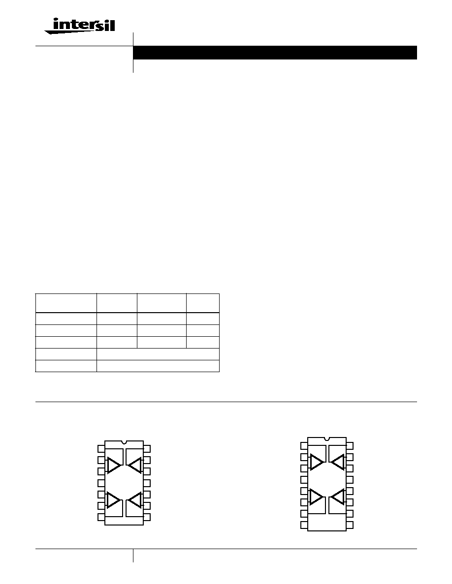
Pinouts
HFA1405 (PDIP, SOIC)
TOP VIEW
HFA1405 (SSOP)
TOP VIEW
Ordering Information
PART NUMBER
TEMP.
RANGE (
o
C)
PACKAGE
PKG. NO.
HFA1405IB
-40 to 85
14 Ld SOIC
M14.15
HFA1405IP
-40 to 85
14 Ld PDIP
E14.3
HFA1405IA
-40 to 85
16 Ld SSOP
M16.15A
HA5025EVAL
High Speed Op Amp DIP Evaluation Board
OPAMPSSOPEVAL1 High Speed Op Amp SSOP Evaluation Board
OUT 1
-IN 1
+IN 1
V+
+IN 2
-IN 2
OUT 2
OUT 4
-IN 4
+IN 4
V-
+IN 3
-IN 3
OUT 3
1
2
3
4
5
6
7
14
13
12
11
10
9
8
+
+
+
-
-
-
+
-
OUT 1
-IN 1
+IN 1
V+
+IN 2
-IN 2
OUT 2
OUT 4
-IN 4
+IN 4
V-
+IN 3
-IN 3
OUT 3
1
2
3
4
5
6
7
16
15
14
13
12
11
10
+
+
+
-
-
-
8
9
NC
NC
+
-
Data Sheet
August 2000
File Number
3604.6
2
Absolute Maximum Ratings
T
A
= 25
o
C
Thermal Information
Voltage Between V+ and V- . . . . . . . . . . . . . . . . . . . . . . . . . . . . 11V
DC Input Voltage . . . . . . . . . . . . . . . . . . . . . . . . . . . . . . . . V
SUPPLY
Differential Input Voltage . . . . . . . . . . . . . . . . . . . . . . . . . . . . . . . 5V
Output Current (Note 2) . . . . . . . . . . . . . . . . .Short Circuit Protected
30mA Continuous
60mA
50% Duty Cycle
ESD Rating
Human Body Model (Per MIL-STD-883 Method 3015.7) . . . 600V
Operating Conditions
Temperature Range . . . . . . . . . . . . . . . . . . . . . . . . . . -40
o
C to 85
o
C
Thermal Resistance (Typical, Note 1)
JA
(
o
C/W)
SOIC Package . . . . . . . . . . . . . . . . . . . . . . . . . . . . .
90
PDIP Package . . . . . . . . . . . . . . . . . . . . . . . . . . . . .
100
SSOP Package . . . . . . . . . . . . . . . . . . . . . . . . . . . .
140
Moisture Sensitivity (see Technical Brief TB363)
All Packages. . . . . . . . . . . . . . . . . . . . . . . . . . . . . . . . . . . . Level 1
Maximum Junction Temperature (Die) . . . . . . . . . . . . . . . . . . . 175
o
C
Maximum Junction Temperature (Plastic Package) . . . . . . . 150
o
C
Maximum Storage Temperature Range . . . . . . . . . . -65
o
C to 150
o
C
Maximum Lead Temperature (Soldering 10s) . . . . . . . . . . . . 300
o
C
(SOIC and SSOP - Lead Tips Only)
CAUTION: Stresses above those listed in "Absolute Maximum Ratings" may cause permanent damage to the device. This is a stress only rating and operation of the
device at these or any other conditions above those indicated in the operational sections of this specification is not implied.
NOTES:
1.
JA
is measured with the component mounted on a low effective thermal conductivity test board in free air. See Tech Brief TB379 for details.
2. Output is short circuit protected to ground. Brief short circuits to ground will not degrade reliability, however continuous (100% duty cycle) output
current must not exceed 30mA for maximum reliability.
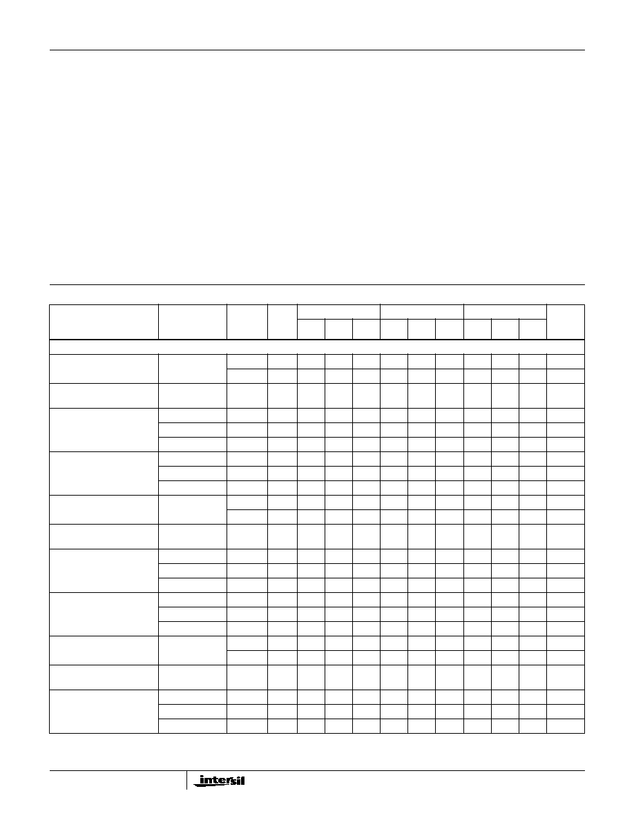
Electrical Specifications
V
SUPPLY
=
±
5V, A
V
= +1, R
F
= 510
,
R
L
= 100
,
Unless Otherwise Specified
PARAMETER
TEST
CONDITIONS
(NOTE 4)
TEST
LEVEL
TEMP
(
o
C)
HFA1405IB (SOIC)
HFA1405IP (PDIP)
HFA1405IA (SSOP)
UNITS
MIN
TYP
MAX
MIN
TYP
MAX
MIN
TYP
MAX
INPUT CHARACTERISTICS
Input Offset Voltage
A
25
-
2
5
-
2
5
-
2
5
mV
A
Full
-
3
8
-
3
8
-
3
8
mV
Average Input Offset
Voltage Drift
B
Full
-
1
10
-
1
10
-
1
10
µ
V/
o
C
Input Offset Voltage
Common-Mode Rejection
Ratio
V
CM
=
±
1.8V
A
25
45
48
-
45
48
-
45
48
-
dB
V
CM
=
±
1.8V
A
85
43
46
-
43
46
-
43
46
-
dB
V
CM
=
±
1.2V
A
-40
43
46
-
43
46
-
43
46
-
dB
Input Offset Voltage
Power Supply Rejection
Ratio
V
PS
=
±
1.8V
A
25
48
52
-
48
52
-
48
52
-
dB
V
PS
=
±
1.8V
A
85
46
48
-
46
48
-
46
48
-
dB
V
PS
=
±
1.2V
A
-40
46
48
-
46
48
-
46
48
-
dB
Non-Inverting Input Bias
Current
A
25
-
6
15
-
6
15
-
6
15
µ
A
A
Full
-
10
25
-
10
25
-
10
25
µ
A
Non-Inverting Input Bias
Current Drift
B
Full
-
5
60
-
5
60
-
5
60
nA/
o
C
Non-Inverting Input Bias
Current Power Supply
Sensitivity
V
PS
=
±
1.8V
A
25
-
0.5
1
-
0.5
1
-
0.5
1
µ
A/V
V
PS
=
±
1.8V
A
85
-
0.8
3
-
0.8
3
-
0.8
3
µ
A/V
V
PS
=
±
1.2V
A
-40
-
0.8
3
-
0.8
3
-
0.8
3
µ
A/V
Non-Inverting Input
Resistance
V
CM
=
±
1.8V
A
25
0.8
1.2
-
0.8
1.2
-
0.8
1.2
-
M
V
CM
=
±
1.8V
A
85
0.5
0.8
-
0.5
0.8
-
0.5
0.8
-
M
V
CM
=
±
1.2V
A
-40
0.5
0.8
-
0.5
0.8
-
0.5
0.8
-
M
Inverting Input Bias Current
A
25
-
2
7.5
-
2
7.5
-
2
7.5
µ
A
A
Full
-
5
15
-
5
15
-
5
15
µ
A
Inverting Input Bias Current
Drift
B
Full
-
60
200
-
60
200
-
60
200
nA/
o
C
Inverting Input Bias Current
Common-Mode Sensitivity
V
CM
=
±
1.8V
A
25
-
3
6
-
3
6
-
3
6
µ
A/V
V
CM
=
±
1.8V
A
85
-
4
8
-
4
8
-
4
8
µ
A/V
V
CM
=
±
1.2V
A
-40
-
4
8
-
4
8
-
4
8
µ
A/V
HFA1405
3
Inverting Input Bias Current
Power Supply Sensitivity
V
PS
=
±
1.8V
A
25
-
2
5
-
2
5
-
2
5
µ
A/V
V
PS
=
±
1.8V
A
85
-
4
8
-
4
8
-
4
8
µ
A/V
V
PS
=
±
1.2V
A
-40
-
4
8
-
4
8
-
4
8
µ
A/V
Inverting Input Resistance
C
25
-
60
-
-
60
-
-
60
-
Input Capacitance
B
25
-
1.4
-
-
2.2
-
-
1.2
-
pF
Input Voltage Common
Mode Range (Implied by
V
IO
CMRR, +R
IN
, and
-I
B-IAS
CMS Tests)
A
25, 85
±
1.8
±
2.4
-
±
1.8
±
2.4
-
±
1.8
±
2.4
-
V
A
-40
±
1.2
±
1.7
-
±
1.2
±
1.7
-
±
1.2
±
1.7
-
V
Input Noise Voltage Density f = 100kHz
B
25
-
3.5
-
-
3.5
-
-
3.5
-
nV/
Hz
Non-Inverting Input Noise
Current Density
f = 100kHz
B
25
-
2.5
-
-
2.5
-
-
2.5
-
pA/
Hz
Inverting Input Noise Current
Density
f = 100kHz
B
25
-
20
-
-
20
-
-
20
-
pA/
Hz
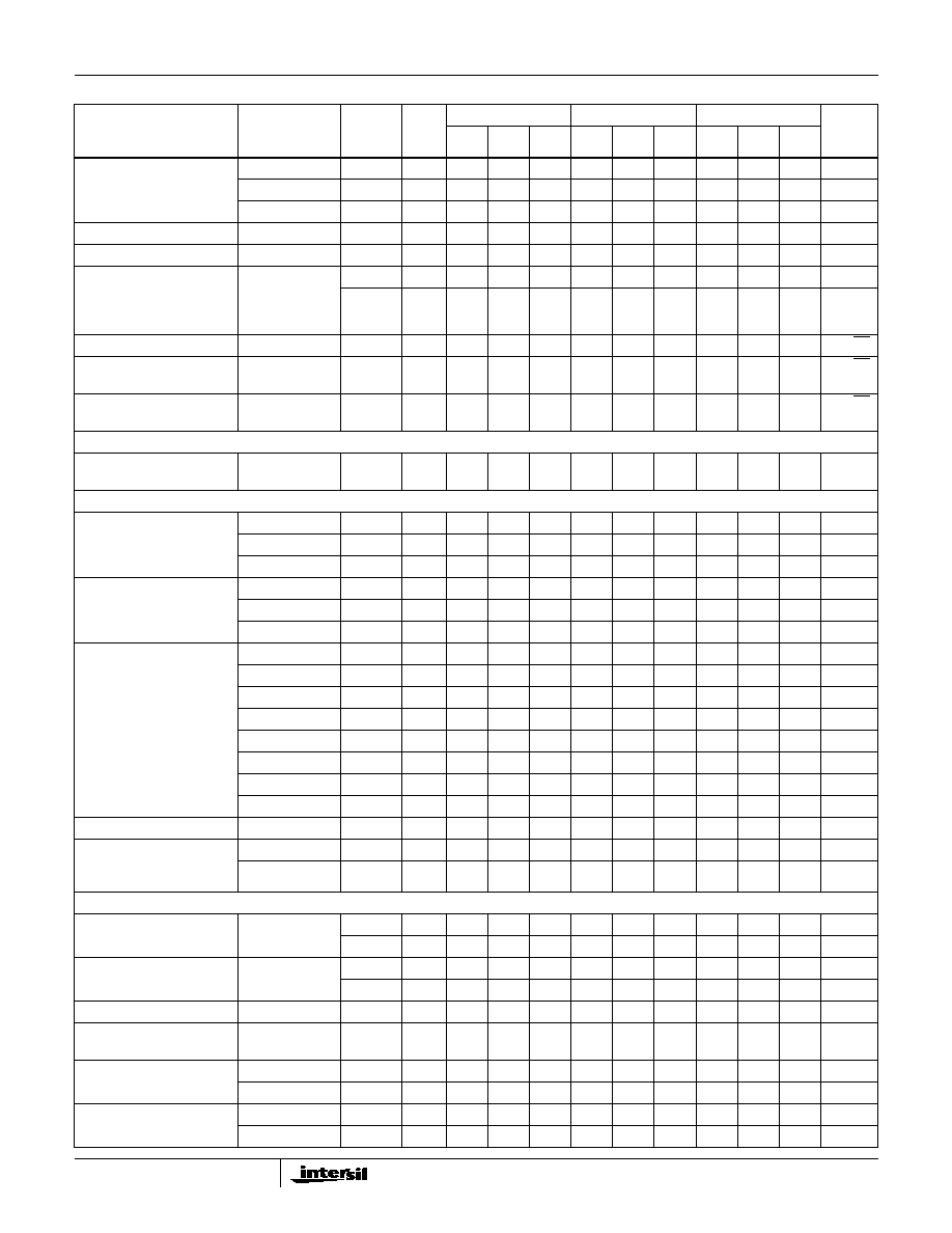
TRANSFER CHARACTERISTICS
Open Loop
Transimpedance Gain
A
V
= -1
C
25
-
500
-
-
500
-
-
500
-
k
AC CHARACTERISTICS (Note 3)
-3dB Bandwidth
(V
OUT
= 0.2V
P-P
,
Notes 3, 5)
A
V
= -1
B
25
-
420
-
-
360
-
-
450
-
MHz
A
V
= +2
B
25
-
560
-
-
400
-
-
675
-
MHz
A
V
= +6
B
25
-
140
-
-
100
-
-
-
-
MHz
Full Power Bandwidth
(V
OUT
= 5V
P-P
,
Notes 3, 5)
A
V
= -1
B
25
-
260
-
-
260
-
-
290
-
MHz
A
V
= +2
B
25
-
165
-
-
165
-
-
190
-
MHz
A
V
= +6
B
25
-
140
-
-
100
-
-
-
-
MHz
Gain Flatness
(V
OUT
= 0.2V
P-P
,
Notes 3, 5)
A
V
= -1, 25MHz
B
25
-
±
0.03
-
-
±
0.04
-
-
±
0.03
-
dB
A
V
= -1, 50MHz
B
25
-
±
0.04
-
-
±
0.04
-
-
±
0.06
-
dB
A
V
= -1, 100MHz
B
25
-
±
0.09
-
-
±
0.06
-
-
±
0.07
-
dB
A
V
= +2, 25MHz
B
25
-
±
0.03
-
-
±
0.04
-
-
±
0.04
-
dB
A
V
= +2, 50MHz
B
25
-
±
0.03
-
-
±
0.04
-
-
±
0.08
-
dB
A
V
= +2, 100MHz
B
25
-
±
0.07
-
-
±
0.06
-
-
±
0.09
-
dB
A
V
= +6, 15MHz
B
25
-
±
0.08
-
-
±
0.08
-
-
-
-
dB
A
V
= +6, 30MHz
B
25
-
±
0.19
-
-
±
0.27
-
-
-
-
dB
Minimum Stable Gain
A
Full
-
1
-
-
1
-
-
1
-
V/V
Crosstalk
(A
V
= +1, All Channels
Hostile, Note 5)
5MHz
B
25
-
-60
-
-
-55
-
-
-59
-
dB
10MHz
B
25
-
-56
-
-
-52
-
-
-56
-
dB
OUTPUT CHARACTERISTICS A
V
= +2 (Note 3), Unless Otherwise Specified
Output Voltage Swing
(Note 5)
A
V
= -1,
R
L
= 100
A
25
±
3
±
3.4
-
±
3
±
3.4
-
±
3
±
3.4
-
V
A
Full
±
2.8
±
3
-
±
2.8
±
3
-
±
2.8
±
3
-
V
Output Current
(Note 5)
A
V
= -1,
R
L
= 50
A
25, 85
50
60
-
50
60
-
50
60
-
mA
A
-40
28
42
-
28
42
-
28
42
-
mA
Output Short Circuit Current
B
25
-
90
-
-
90
-
-
90
-
mA
Closed Loop Output
Impedance
B
25
-
0.2
-
-
0.2
-
-
0.2
-
Second Harmonic Distortion
(V
OUT
= 2V
P-P
, Note 5)
10MHz
B
25
-
-51
-
-
-51
-
-
-51
-
dBc
20MHz
B
25
-
-46
-
-
-46
-
-
-46
-
dBc
Third Harmonic Distortion
(V
OUT
= 2V
P-P
, Note 5)
10MHz
B
25
-
-63
-
-
-63
-
-
-63
-
dBc
20MHz
B
25
-
-56
-
-
-56
-
-
-56
-
dBc
Electrical Specifications
V
SUPPLY
=
±
5V, A
V
= +1, R
F
= 510
,
R
L
= 100
,
Unless Otherwise Specified (Continued)
PARAMETER
TEST
CONDITIONS
(NOTE 4)
TEST
LEVEL
TEMP
(
o
C)
HFA1405IB (SOIC)
HFA1405IP (PDIP)
HFA1405IA (SSOP)
UNITS
MIN
TYP
MAX
MIN
TYP
MAX
MIN
TYP
MAX
HFA1405
4
Application Information
Performance Differences Between Packages
The amplifiers comprising the HFA1405 are high frequency
current feedback amplifiers. As such, they are sensitive to
feedback capacitance which destabilizes the op amp and
causes overshoot and peaking. Unfortunately, the standard
quad op amp pinout places the amplifier's output next to its
inverting input, thus making the package capacitance an
unavoidable parasitic feedback capacitor. The larger
parasitic capacitance of the PDIP requires an inherently
more stable amplifier, which yields a PDIP device with lower
performance than the SOIC and SSOP devices - see
Electrical Specification tables for details.
Because of these performance differences, designers
should evaluate and breadboard with the same package
style to be used in production.
Note that the "Typical Performance Curves" section has
separate pulse and frequency response graphs for each
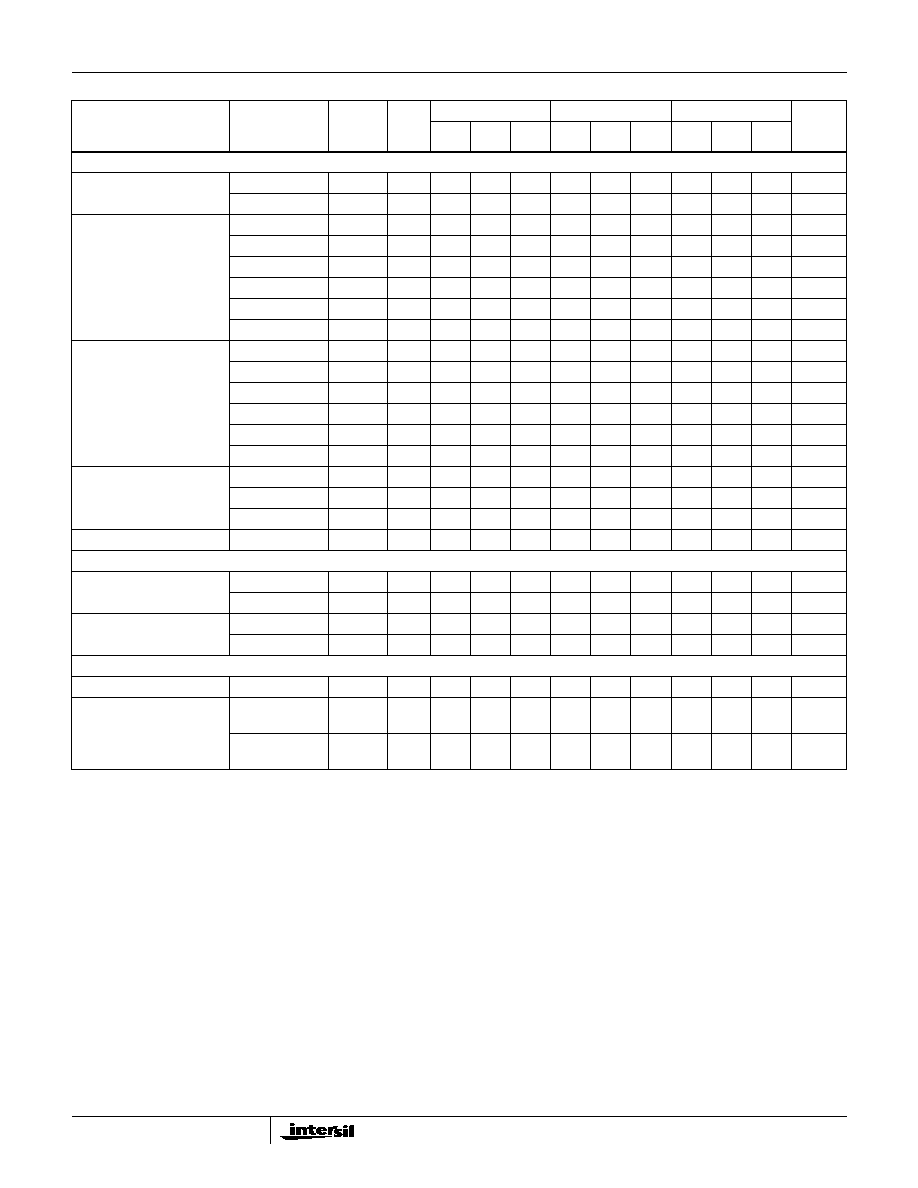
TRANSIENT CHARACTERISTICS A
V
= +2 (Note 3), Unless Otherwise Specified
Rise and Fall Times
(V
OUT
= 0.5V
P-P
, Note 3)
A
V
= +2
B
25
-
0.8
-
-
0.9
-
-
0.6
-
ns
A
V
= +6
B
25
-
2.9
-
-
4
-
-
-
-
ns
Overshoot
(V
OUT
= 0.5V
P-P
, V
IN
t
RISE
= 1ns, Notes 3, 6)
A
V
= -1, +OS
B
25
-
7
-
-
3
-
-
2
-
%
A
V
= -1, -OS
B
25
-
8
-
-
13
-
-
8
-
%
A
V
= +2, +OS
B
25
-
5
-
-
7
-
-
5
-
%
A
V
= +2, -OS
B
25
-
10
-
-
11
-
-
5
-
%
A
V
= +6, +OS
B
25
-
2
-
-
2
-
-
-
-
%
A
V
= +6, -OS
B
25
-
2
-
-
2
-
-
-
-
%
Slew Rate
(V
OUT
= 5V
P-P
,
Notes 3, 5)
A
V
= -1, +SR
B
25
-
2500
-
-
2500
-
-
2900
-
V/
µ
s
A
V
= -1, -SR
B
25
-
1900
-
-
1900
-
-
2500
-
V/
µ
s
A
V
= +2, +SR
B
25
-
1700
-
-
1600
-
-
2100
-
V/
µ
s
A
V
= +2, -SR
B
25
-
1700
-
-
1400
-
-
1900
-
V/
µ
s
A
V
= +6, +SR
B
25
-
1500
-
-
1000
-
-
-
-
V/
µ
s
A
V
= +6, -SR
B
25
-
1100
-
-
1000
-
-
-
-
V/
µ
s
Settling Time
(V
OUT
= +2V to 0V Step,
Note 5)
To 0.1%
B
25
-
23
-
-
23
-
-
30
-
ns
To 0.05%
B
25
-
30
-
-
30
-
-
33
-
ns
To 0.025%
B
25
-
37
-
-
40
-
-
50
-
ns
Overdrive Recovery Time
V
IN
=
±
2V
B
25
-
8.5
-
-
8.5
-
-
8.5
-
ns
VIDEO CHARACTERISTICS
A
V
= +2 (Note 3), Unless Otherwise Specified
Differential Gain
(f = 3.58MHz)
R
L
= 150
B
25
-
0.02
-
-
0.03
-
-
0.02
-
%
R
L
= 75
B
25
-
0.03
-
-
0.06
-
-
0.03
-
%
Differential Phase
(f = 3.58MHz)
R
L
= 150
B
25
-
0.03
-
-
0.03
-
-
0.03
-
Degrees
R
L
= 75
B
25
-
0.06
-
-
0.06
-
-
0.06
-
Degrees
POWER SUPPLY CHARACTERISTICS
Power Supply Range
C
25
±
4.5
-
±
5.5
±
4.5
-
±
5.5
±
4.5
-
±
5.5
V
Power Supply Current
(Note 5)
A
25
-
5.8
6.1
-
5.8
6.1
-
5.8
6.1
mA/Op
Amp
A
Full
-
5.9
6.3
-
5.9
6.3
-
5.9
6.3
mA/Op
Amp
NOTES:
3. The optimum feedback resistor depends on closed loop gain and package type. See the "Optimum Feedback Resistor" table in the Application
Information section for details.
4. Test Level: A. Production Tested; B. Typical or Guaranteed Limit Based on Characterization; C. Design Typical for Information Only.
5. See Typical Performance Curves for more information.
6. Undershoot dominates for output signal swings below GND (e.g., 2V
P-P
), yielding a higher overshoot limit compared to the V
OUT
= 0V to 2V
condition. See the "Application Information" section for details.
Electrical Specifications
V
SUPPLY
=
±
5V, A
V
= +1, R
F
= 510
,
R
L
= 100
,
Unless Otherwise Specified (Continued)
PARAMETER
TEST
CONDITIONS
(NOTE 4)
TEST
LEVEL
TEMP
(
o
C)
HFA1405IB (SOIC)
HFA1405IP (PDIP)
HFA1405IA (SSOP)
UNITS
MIN
TYP
MAX
MIN
TYP
MAX
MIN
TYP
MAX
HFA1405
5
package type. Graphs not labeled with a specific package
type are applicable to all packages.
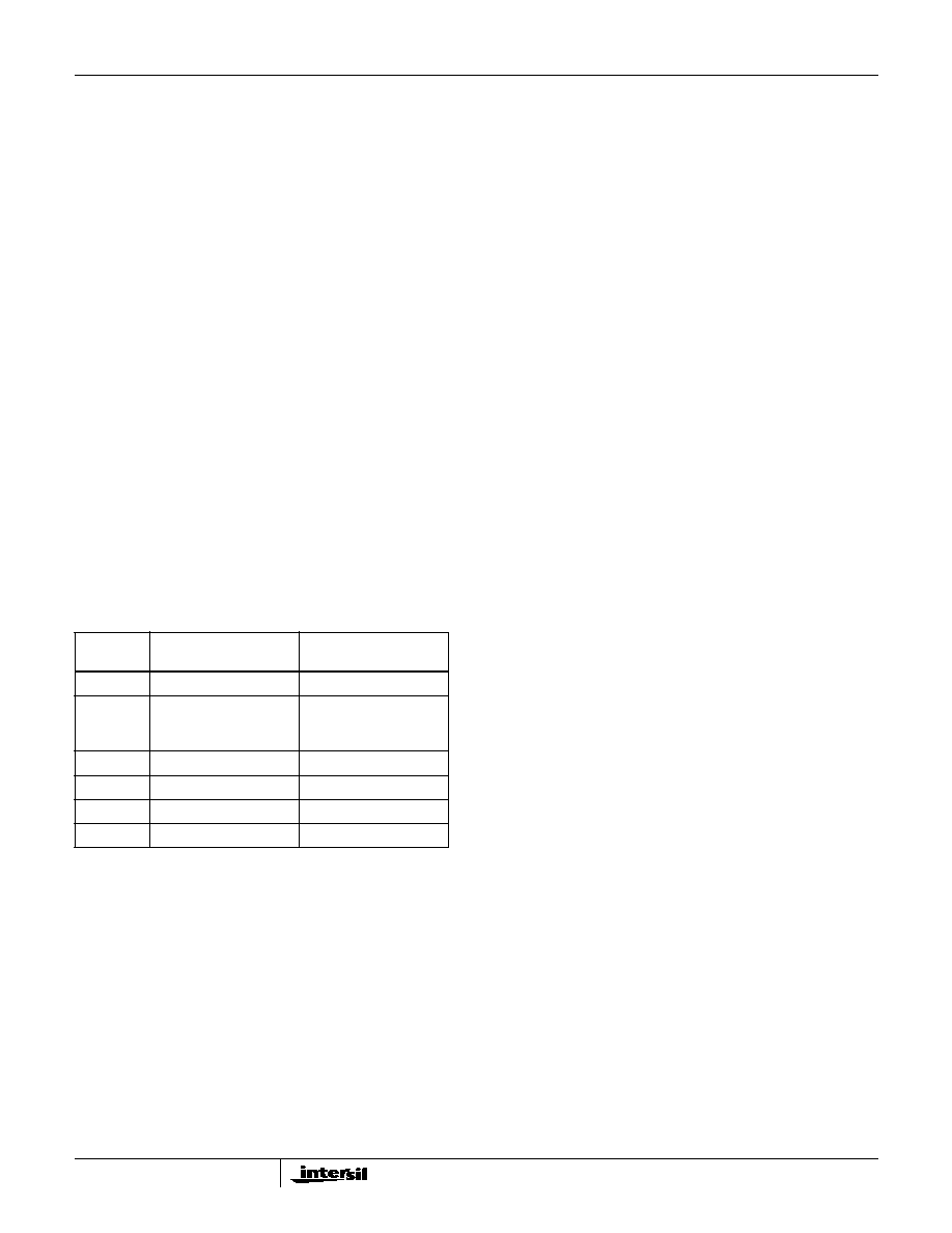
Optimum Feedback Resistor
Although a current feedback amplifier's bandwidth
dependency on closed loop gain isn't as severe as that of a
voltage feedback amplifier, there can be an appreciable
decrease in bandwidth at higher gains. This decrease may
be minimized by taking advantage of the current feedback
amplifier's unique relationship between bandwidth and R
F
.
All current feedback amplifiers require a feedback resistor,
even for unity gain applications, and R
F
, in conjunction with
the internal compensation capacitor, sets the dominant pole
of the frequency response. Thus, the amplifier's bandwidth is
inversely proportional to R
F
. The HFA1405 design is
optimized for R
F
= 402
/510
/681
(PDIP/SOIC/SSOP) at
a gain of +2. Decreasing R
F
decreases stability, resulting in
excessive peaking and overshoot (Note: Capacitive
feedback causes the same problems due to the feedback
impedance decrease at higher frequencies). However, at
higher gains the amplifier is more stable so R
F
can be
decreased in a trade-off of stability for bandwidth.
The table below lists recommended R
F
values for various
gains, and the expected bandwidth. For good channel-to-
channel gain matching, it is recommended that all resistors
(termination as well as gain setting) be
±
1% tolerance or
better.
NOTE:
R
F
= 500
is not the optimum value. It was chosen to
match the R
F
of the CLC414 and CLC415, for performance
comparison purposes. Performance at A
V
= +6 may be increased by
reducing R
F
below 500
.
Non-inverting Input Source Impedance
For best operation, the DC source impedance seen by the
non-inverting input should be
50
.
This is especially
important in inverting gain configurations where the non-
inverting input would normally be connected directly to GND.
Pulse Undershoot
The HFA1405 utilizes a quasi-complementary output stage
to achieve high output current while minimizing quiescent
supply current. In this approach, a composite device
replaces the traditional PNP pulldown transistor. The
composite device switches modes after crossing 0V,
resulting in added distortion for signals swinging below
ground, and an increased undershoot on the negative
portion of the output waveform (see Figure 8 and Figure 11).
This undershoot isn't present for small bipolar signals, or
large positive signals (see Figure 6 and Figure 7).
PC Board Layout
The frequency response of this amplifier depends greatly on
the amount of care taken in designing the PC board. The
use of low inductance components such as chip
resistors and chip capacitors is strongly recommended,
while a solid ground plane is a must!
Attention should be given to decoupling the power supplies.
A large value (10
µ
F) tantalum in parallel with a small value
(0.1
µ
F) chip capacitor works well in most cases.
Terminated microstrip signal lines are recommended at the
input and output of the device. Capacitance, parasitic or
planned, connected to the output must be minimized, or
isolated as discussed in the next section.
Care must also be taken to minimize the capacitance to
ground at the amplifier's inverting input (-IN). The larger this
capacitance, the worse the gain peaking, resulting in pulse
overshoot and eventual instability. To reduce this
capacitance the designer should remove the ground plane
under traces connected to -IN, and keep connections to -IN
as short as possible.
An example of a good high frequency layout is the
Evaluation Boards shown in Figures 3 and 5.
Driving Capacitive Loads
Capacitive loads, such as an A/D input, or an improperly
terminated transmission line will degrade the amplifier's
phase margin resulting in frequency response peaking and
possible oscillations. In most cases, the oscillation can be
avoided by placing a resistor (R
S
) in series with the output
prior to the capacitance.
Figure 1 details starting points for the selection of this
resistor. The points on the curve indicate the R
S
and C
L
combinations for the optimum bandwidth, stability, and
settling time, but experimental fine tuning is recommended.
Picking a point above or to the right of the curve yields an
overdamped response, while points below or left of the curve
indicate areas of underdamped performance.
R
S
and C
L
form a low pass network at the output, thus limiting
system bandwidth well below the amplifier bandwidth of
560MHz. By decreasing R
S
as C
L
increases (as illustrated in
the curve), the maximum bandwidth is obtained without
TABLE 1. OPTIMUM FEEDBACK RESISTOR
GAIN
(A
CL
)
R
F
(
)
PDIP/SOIC/SSOP
BANDWIDTH (MHz)
PDIP/SOIC/SSOP
-1
310/360/432
360/420/450
+1
510 (+R
S
= 510)/
464 (+R
S
= 649)/
681 (+R
S
= 806)
300/375/330
+2
402/510/681
400/560/675
+5
NA/200/649
NA/330/200
+6
500/500/NA (Note)
100/140/NA
+10
NA/180/681
NA/140/120
HFA1405