CAUTION: These devices are sensitive to electrostatic discharge; follow proper IC Handling Procedures.
1-888-INTERSIL or 321-724-7143
|
Intersil (and design) is a registered trademark of Intersil Americas Inc.
Copyright © Intersil Americas Inc. 2002. All Rights Reserved
3-33
Æ
HFA-0003,
HFA-0003L
Ultra High Speed Comparator
September 1998
Description
The HFA-0003/0003L are monolithic, ultra high speed,
voltage comparators. These comparators combine a low
input offset voltage (1.0mV) with a low propagation delay
(2.0ns) to achieve a large dynamic input range. The low off-
set voltage also makes these comparators ideally suited for
high speed, precision analog-to-digital processing applica-
tions. The circuits have differential analog inputs, and pro-
vide complementary, ECL compatible (10K and 100K) logic
outputs. The outputs are capable of supplying the current
required by terminated 50
transmission lines. Both outputs
are open emitter structures, requiring external pull-down
resistors. The recommended circuit is 50
connected to -
2.0V, but any equivalent ECL termination circuit may be
used.
The HFA-0003L is a latched version of the HFA-0003. The
latch function allows the HFA-0003L to operate in sample-
hold or track-hold modes, when synchronous detection is
required. The Latch Enable (LE) input can be driven by a
standard ECL gate. See the Applications section for more
information on this feature.
The HFA-0003L also has an additional feature, user
programmable hysteresis. By connecting a resistor from the
HYS pin to GND the user can select up to 20mV of input
hysteresis. See the Applications section for more informa-
tion on this feature.
The HFA-0003 is pin compatible with the MAX9690, and
SP9680 while providing improved performance. The HFA-
0003L is pin compatible with the MAX9685, AD96685,
SP9685, HCMP96850, and the VC7695 while providing
improved performance.
Features
∑ Low Propagation Delay (0003/0003L) . . . . . . . . . . 2.0/2.1ns
∑ Low Latch Set Up Time . . . . . . . . . . . . . . . . . . . . . . . . 0.8ns
∑ Low Offset Voltage, Drift Coefficient . . . . . 1.0mV, 4
µ
V/
o
C
∑ Wide Common Mode Range . . . . . . . . . . . . . . . . +5.2/-2.8V
∑ Low Power Dissipation . . . . . . . . . . . . . . . . . . . . . . 200mW
∑ Large Differential Input Resistance . . . . . . . . . . . . . . .1M
∑ Complementary ECL Outputs; 50
Driving Capability
∑ Resistor Programmable Hysteresis with HFA-0003L
∑ Pin Compatible with MAX9690/9685 and AD96685
∑ Available in SOIC
Applications
∑ Window Detector
∑ High Speed Peak Detector
∑ High Speed Threshold Detector
∑ High Speed Data Acquisition Systems
∑ Fiber Optic Decision Circuits
∑ High Speed Phase Detector
∑ Frequency Counter
Part Number Information
PART
NUMBER
TEMPERATURE
RANGE
PACKAGE
HFA1-0003L-5
0
o
C to +75
o
C
16 Lead Ceramic Sidebraze DIP
HFA1-0003L-9
-40
o
C to +85
o
C
16 Lead Ceramic Sidebraze DIP
HFA2-0003L-5
0
o
C to +75
o
C
10 Pin CAN
HFA2-0003L-9
-40
o
C to +85
o
C
10 Pin CAN
HFA3-0003-5
0
o
C to +75
o
C
8 Lead Plastic DIP
HFA3-0003-9
-40
o
C to +85
o
C
8 Lead Plastic DIP
HFA3-0003L-5
0
o
C to +75
o
C
16 Lead Plastic DIP
HFA3-0003L-9
-40
o
C to +85
o
C
16 Lead Plastic DIP
File Number
2749.5
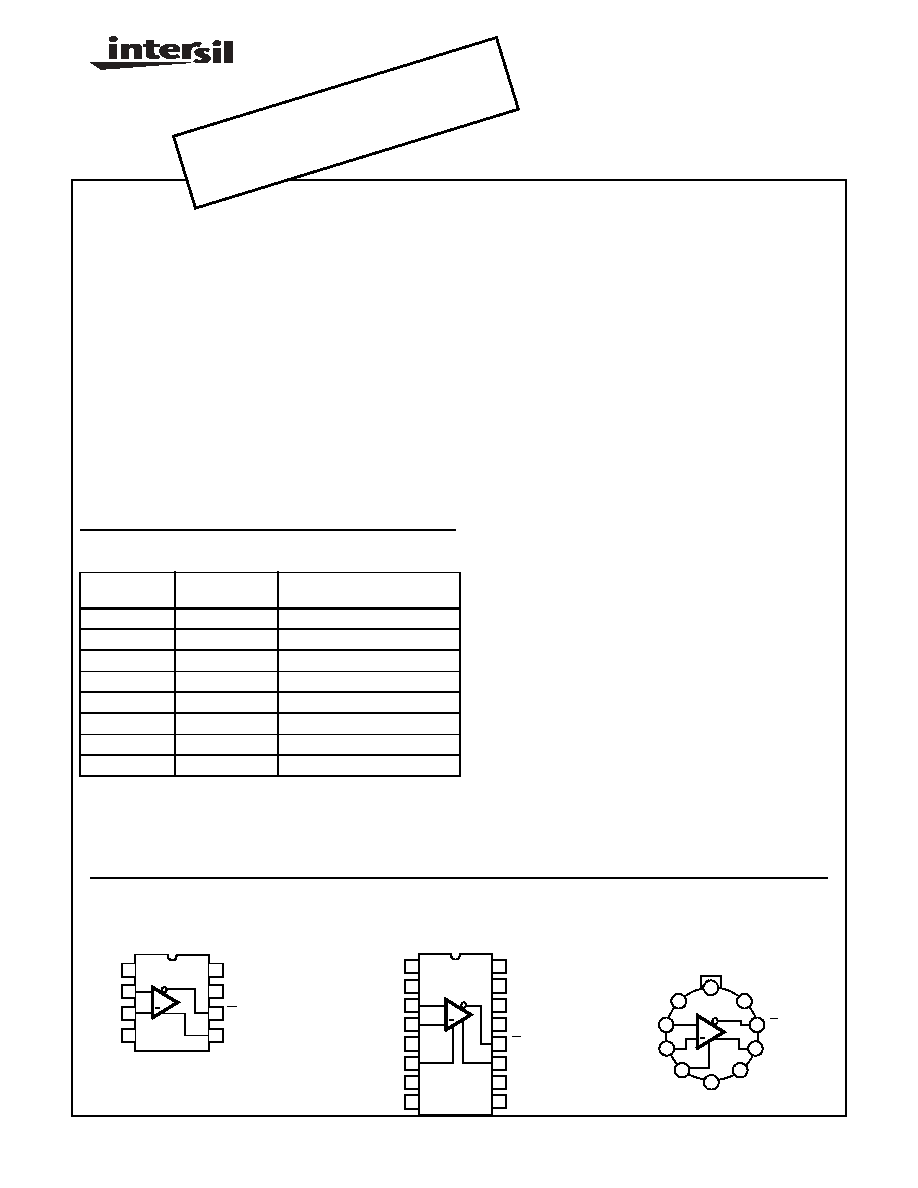
Pinouts
HFA-0003 (PDIP, CDIP, SOIC)
TOP VIEW
HFA-0003L (PDIP, CDIP, 150 mil SOIC)
TOP VIEW
HFA-0003L (TO-100 CAN)
TOP VIEW
2
3
4
1
7
6
5
8
+
V+
+IN
V-
GND 1 (DIGITAL)
Q OUT
Q OUT
GND 2 (ANALOG)
-IN
14
15
16
9
13
12
11
10
1
2
3
4
5
7
6
8
GND1
-IN
+IN
V-
LE
NC
V+
NC
GND 2
NC
NC
NC
Q OUT
Q OUT
NC
HYS
+
(DIGITAL)
(ANALOG)
2
4
6
1
7
5
8
+
9
3
10
GND 2
Q OUT
Q OUT
HYS
V-
LE
-IN
+IN
V+
GND1
(ANALOG)
(DIGITAL)
DB
5
0
0
OBS
OLE
TE P
ROD
UCT
No R
ecom
men
ded
Repl
acem
ent
or Co
ntac
t our
Tec
hnic
al Su
ppor
t Cen
ter a
t
1-88
8-INT
ERS
IL or
www
.inte
rsil.c
om/t
sc
3-34
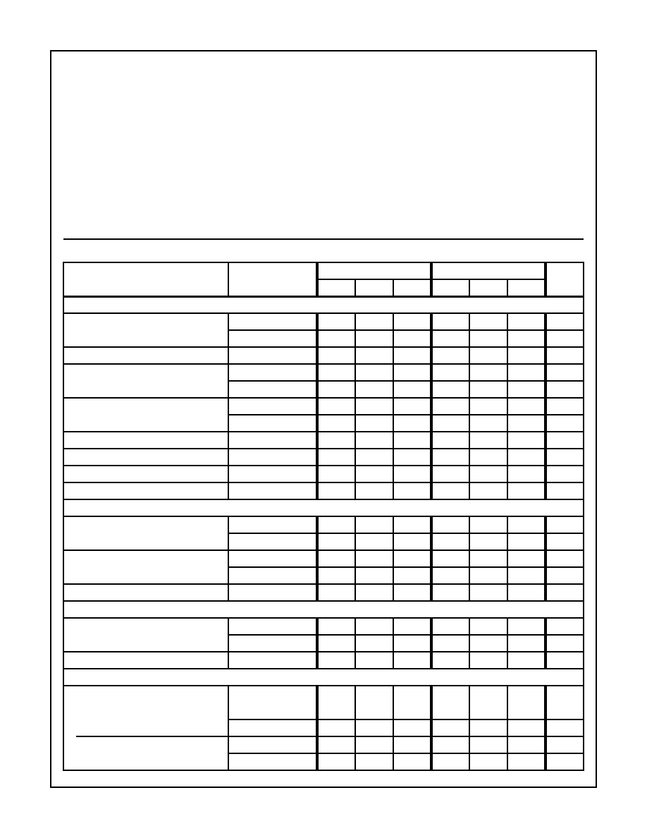
Specifications HFA-0003, HFA-0003L
Absolute Maximum Ratings
(Note 1)
Operating Conditions
Supply Voltage (GND to V+) . . . . . . . . . . . . . . . . . . . . . . . . . . . . 8V
Supply Voltage (GND to V-) . . . . . . . . . . . . . . . . . . . . . . . . . . . . 18V
Voltage Between V+ and V- Terminals . . . . . . . . . . . . . . . . . . . 20V
Differential Input Voltage . . . . . . . . . . . . . . . . . . . . . . . . . . . . . . 5.5V
Input Voltage
. . . . . . . . . . . . . . . . . . . . . . . . . . . . . . . . . . . . . . . . . . . . ±
5V
Differential Ground Voltage (GND1 to GND2)
. . . . . . . . . . . . . . . . ±
1V
Short Duration Output Current (Note 2) . . . . . . . . . . . . . . . . . -35mA
Junction Temperature. . . . . . . . . . . . . . . . . . . . . . . . . . . . . . +175
o
C
Junction Temperature (Plastic Package) . . . . . . . . . . . . . . . +150
o
C
Lead Temperature (Soldering 10 Sec.) . . . . . . . . . . . . . . . . +300
o
C
Operating Temperature Range
HFA-0003/HFA-0003L-9 . . . . . . . . . . . . . . . . -40
o
C
T
A
+85
o
C
HFA-0003/HFA-0003L-5 . . . . . . . . . . . . . . . . . . 0
o
C
T
A
+75
o
C
Storage Temperature Range . . . . . . . . . . . . . -65
o
C
T
A
+150
o
C
Thermal Package Characteristics (
o
C/W)
JA
JC
8 Lead Ceramic Sidebrazed DIP . . . . . . .
75
13
8 Lead Plastic DIP . . . . . . . . . . . . . . . . . .
96
34
8 Lead SOIC . . . . . . . . . . . . . . . . . . . . . .
157
43
16 Lead Ceramic Sidebrazed DIP . . . . . .
75
13
16 Lead Plastic DIP . . . . . . . . . . . . . . . . .
92
32
16 Lead SOIC . . . . . . . . . . . . . . . . . . . . .
114
35
TO-100 Metal CAN . . . . . . . . . . . . . . . . .
108
32
CAUTION: Stresses above those listed in "Absolute Maximum Ratings" may cause permanent damage to the device. This is a stress only rating and operation
of the device at these or any other conditions above those indicated in the operational sections of this specification is not implied.
Electrical Specifications
V+ = 5V, V- = -5.2V, R
L
= 50
to -2V, Unless Otherwise Specified
PARAMETER
TEMPERATURE
HFA-0003-5/-9
HFA-0003L-5/-9
UNITS
MIN
TYP
MAX
MIN
TYP
MAX
INPUT CHARACTERISTICS
Input Offset Voltage (V
OS
)
+25
o
C
-
1
3
-
1
3
mV
Full
-
-
4
-
-
4
mV
Average Offset Voltage Drift (Note 8)
Full
-
-
4
-
-
4
µ
V/
o
C
Input Bias Current
+25
o
C
-
5
8
-
5
8
µ
A
Full
-
8
13
-
8
13
µ
A
Input Offset Current
+25
o
C
-
0.15
0.2
-
0.15
0.2
µ
A
Full
-
-
0.3
-
-
0.3
µ
A
Common Mode Range
Full
-2.8
-
+5.2
-2.8
-
+5.2
V
Differential Input Resistance
+25
o
C
-
1
-
-
1
-
M
Common Mode Input Resistance
+25
o
C
-
9.5
-
-
9.5
-
M
Input Capacitance
+25
o
C
-
1
-
-
1
-
pF
TRANSFER CHARACTERISTICS
Large Signal Voltage Gain
+25
o
C
-
3100
-
-
3100
-
V/V
Full
-
1200
-
-
1200
-
V/V
Common Mode Rejection Ratio
(Note 3)
+25
o
C
70
75
-
70
75
-
dB
Full
70
-
-
70
-
-
dB
Tracking Bandwidth (Note 4)
+25
o
C
-
270
-
-
270
-
MHz
SWITCHING CHARACTERISTICS
Propagation Delay Input to Output
(t
PD
)(Notes 5, 8, 9)
+25
o
C
-
2.0
2.4
-
2.1
2.6
ns
Full
-
-
2.8
-
-
3.0
ns
Maximum Dispersion (Notes 6, 8)
Full
-
-
200
-
-
200
ps
OUTPUT CHARACTERISTICS
Output Voltage Level:
Logic Low (V
OL
)
+25
o
C
-
-1.83
-1.65
-
-1.83
-1.65
V
Full
-
-1.83
-1.57
-
-1.83
-1.57
V
Logic High (V
OH
)
+25
o
C
-0.938
-0.85
-
-0.938
-0.85
-
V
Full
-1.05
-0.96
-
-1.05
-0.96
-
V
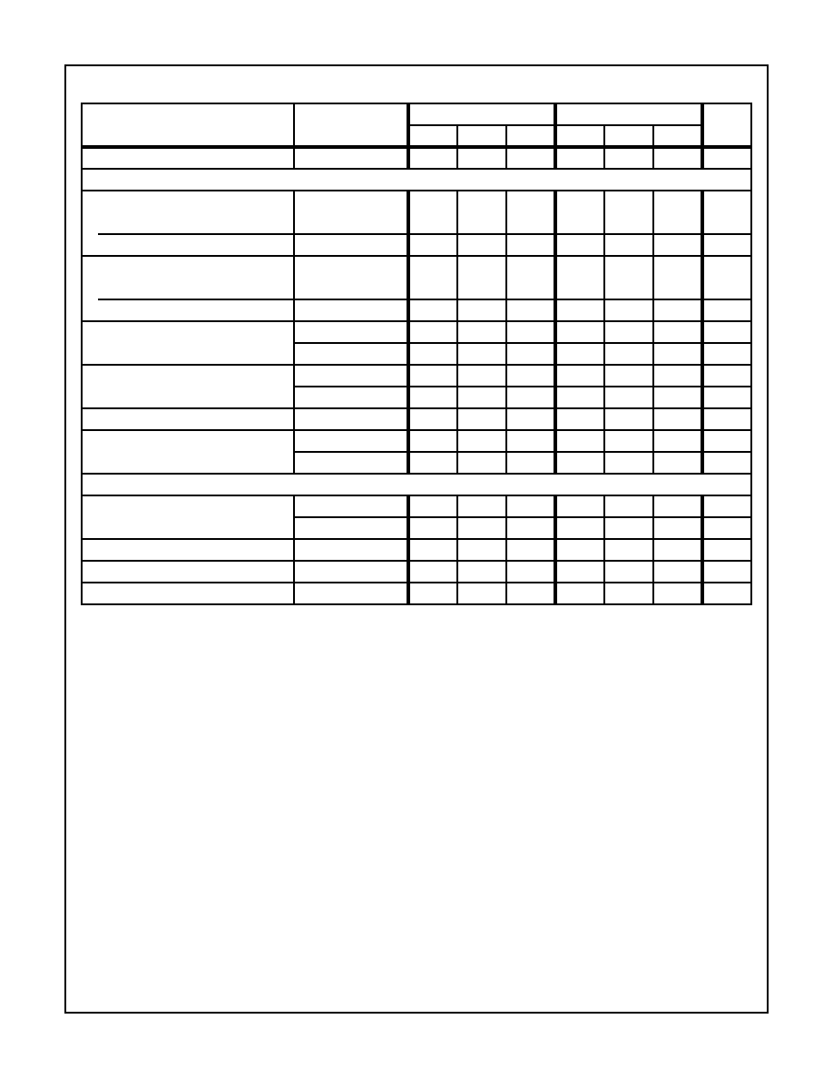
3-35
Specifications HFA-0003, HFA-0003L
Continuous Output Current (Note 2)
Full
-
-
-30
-
-
-30
mA
LATCH CHARACTERISTICS (HFA-0003L ONLY)
LE Input Voltage Level:
Logic Low (V
IL
)
Full
-
-
-
-
-
-1.475
V
Logic High (V
IH
)
Full
-
-
-
-1.105
-
-
V
LE Input Current Level:
Logic Low (V
IL
= -1.85V)
Full
-
-
-
-
0.06
0.5
µ
A
Logic High (V
IH
= -0.81V)
Full
-
-
-
-
11
20
µ
A
Propagation Delay from LE to Output (t
P-
DL
) (Notes 5, 8, 9)
+25
o
C
-
-
-
-
2.2
2.7
ns
Full
-
-
-
-
2.6
3.1
ns
Minimum Set-Up Time (t
S
) (Notes 8, 9)
+25
o
C
-
-
-
-
0.8
1.2
ns
Full
-
-
-
-
-
1.5
ns
Minimum Hold Time (t
H
) (Notes 8, 9)
Full
-
-
-
-
0.5
1.0
ns
Minimum LE Pulse Width (t
PW
)
(Notes 8, 9)
+25
o
C
-
-
-
-
0.9
0.95
ns
Full
-
-
-
-
-
1.1
ns
POWER SUPPLY
PSRR (Note 7)
+25
o
C
70
80
-
70
80
-
dB
Full
65
-
-
65
-
-
dB
I
CC
Full
-
11
13
-
11
13
mA
I
EE
Full
-
19
22
-
19
22
mA
Power Dissipation
Full
-
-
200
-
-
200
mW
NOTES:
1. Absolute maximum ratings are limiting values, applied individually, beyond which the servicability of the circuit may be impaired. Func-
tional operation under any of these conditions is not necessarily implied. Exposure to absolute maximum rating conditions may affect
device reliability.
2. Outputs have no sink current (+I) capability, since they are open emitter NPN transistors.
3. -2.0V
V
CM
+4.0V.
4. Tracking Bandwidth (TBW) is defined as the maximum input frequency at which the outputs still switch between V
OL
and V
OH
.
V
IN
= 15mVp-p sinewave centered on 0V.
5. V
IN
= 100mV. V
OD
is the amount of input overdrive.
6. Dispersion is defined as the change in propagation delay for input overdrives between 0.1V and 1.0V.
7. +4.5V
V+
+5.5V or -6.2V
V-
-4.7V.
8. This parameter is not tested. It is guaranteed by design, and by device characterization.
9. V
OD
= 10mV.
Electrical Specifications
V+ = 5V, V- = -5.2V, R
L
= 50
to -2V, Unless Otherwise Specified (Continued)
PARAMETER
TEMPERATURE
HFA-0003-5/-9
HFA-0003L-5/-9
UNITS
MIN
TYP
MAX
MIN
TYP
MAX
3-36
HFA-0003, HFA-0003L
Applications Information
HFA-0003L Latch Functionality
The Latch Enable (LE) pin of the HFA-0003L controls the
function of the on chip latch. When the LE input is at an ECL
Logic 1, the latch is open (transparent) and the comparator
functions normally. When the LE input switches to a Logic 0,
the outputs are latched in unambiguous states dependant on
the current input state, providing the set-up and hold times
are met. If the latch function is not utilized, the LE input must
be connected to an ECL Logic 1 (e.g. GND).
HFA-0003L Hysteresis Functionality
To improve performance in systems with slow transition
times, and/or high noise levels, the HFA-0003L allows the
user to easily set the amount of input hysteresis. The hyste-
resis level is set by the current flowing into the HYS input;
the larger the current the larger the level of hysteresis. This
current is provided by connecting a resistor (R
H
) between
the HYS pin and GND, and it is recommended that the input
current not exceed 1mA. The input current can be approxi-
mated from the following formula:
The table below gives approximate levels of hysteresis for
some values of I
H
, at T
A
= +25
o
C.
If the hysteresis function isn't used, the HYS input may be
left floating, or may be connected to V-. The HYS input
MUST NEVER BE CONNECTED directly to GND or V+, as
device damage will occur. Before inserting an HFA-0003L
into a competitor socket, the user must ensure that the cor-
responding socket pin is a true no connect (i.e. is floating).
I
H
(mA)
0.2
0.4
0.6
0.8
1.0
HYS (mV)
1
4
8
13
22
IH
GND
V-
( )
0.7V
≠
≠
RH
-------------------------------------------------
=
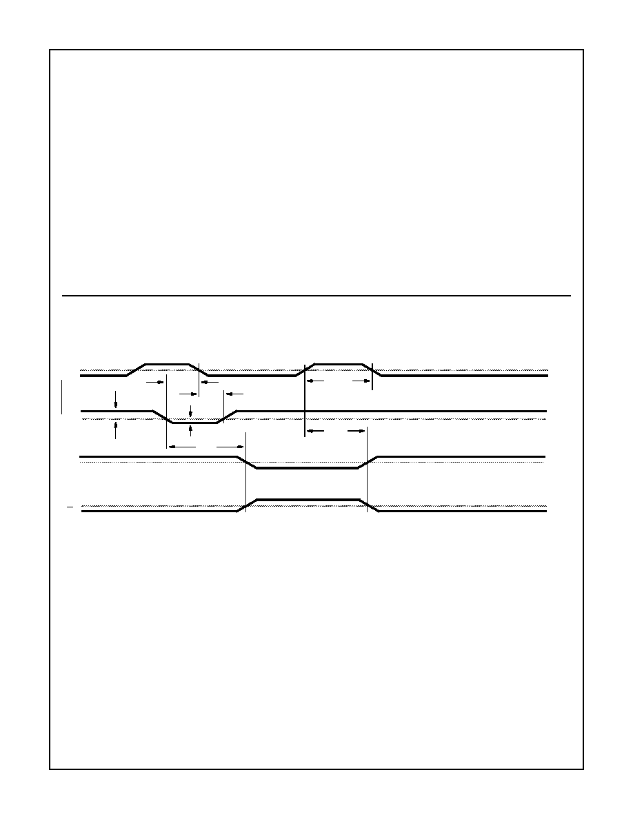
Timing Diagram
Q
tPD
50%
LE
tS
COMPARE
LATCHED
50%
IN
tH
V
IN
V
OD
tPD
L
V
OS
Q
50%
tPW