 | –≠–ª–µ–∫—Ç—Ä–æ–Ω–Ω—ã–π –∫–æ–º–ø–æ–Ω–µ–Ω—Ç: HFA3101BZ | –°–∫–∞—á–∞—Ç—å:  PDF PDF  ZIP ZIP |

1
Æ
FN3663.5
HFA3101
Gilbert Cell UHF Transistor Array
The HFA3101 is an all NPN transistor array configured as a
Multiplier Cell. Based on Intersil's bonded wafer UHF-1 SOI
process, this array achieves very high f
T
(10GHz) while
maintaining excellent h
FE
and V
BE
matching characteristics
that have been maximized through careful attention to circuit
design and layout, making this product ideal for
communication circuits. For use in mixer applications, the
cell provides high gain and good cancellation of 2nd order
distortion terms.
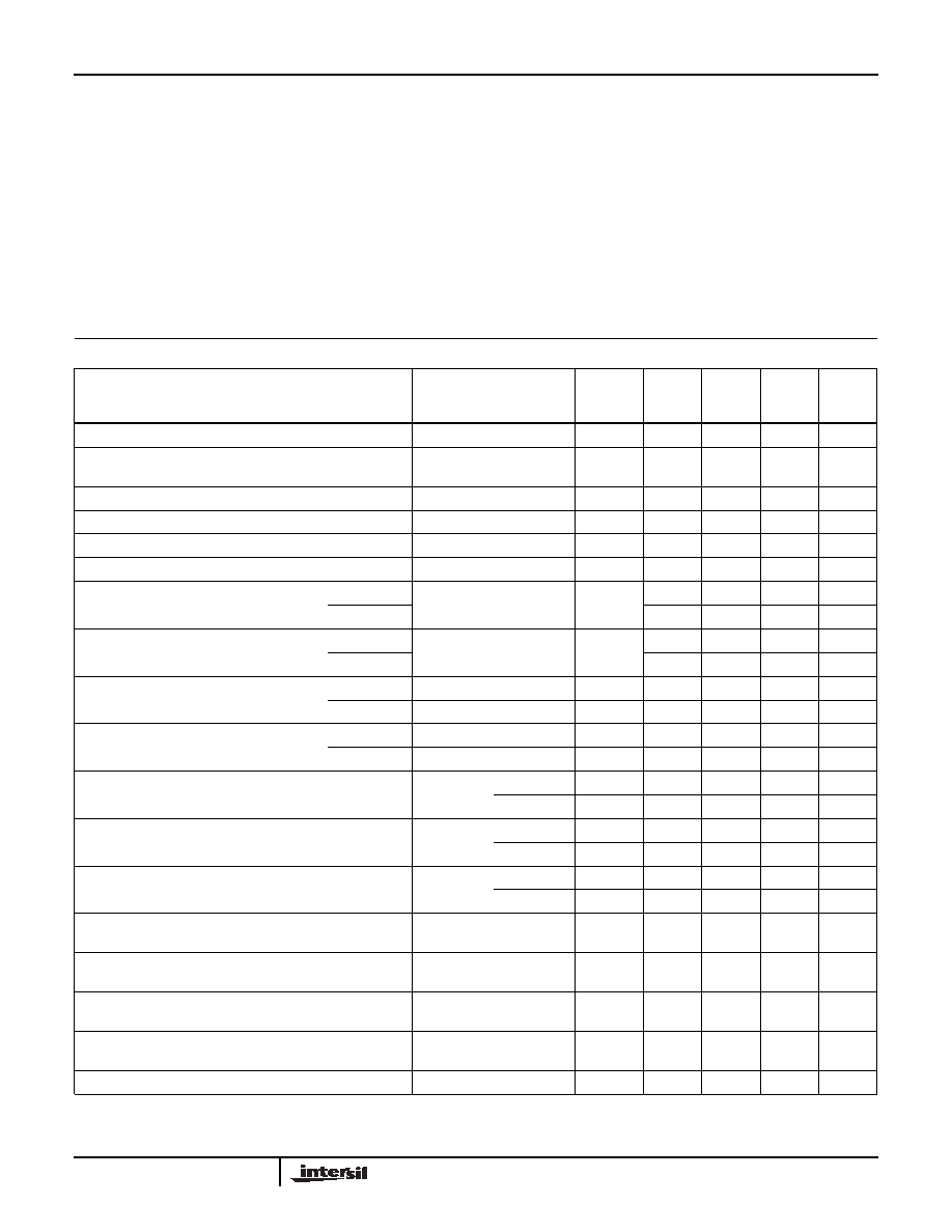
Pinout
HFA3101
(SOIC)
TOP VIEW
Features
∑
Pb-free Available as an Option
∑ High Gain Bandwidth Product (f
T
) . . . . . . . . . . . . . 10GHz
∑ High Power Gain Bandwidth Product . . . . . . . . . . . . 5GHz
∑ Current Gain (h
FE
) . . . . . . . . . . . . . . . . . . . . . . . . . . . . . 70
∑ Low Noise Figure (Transistor) . . . . . . . . . . . . . . . . . 3.5dB
∑ Excellent h
FE
and V
BE
Matching
∑ Low Collector Leakage Current . . . . . . . . . . . . . . <0.01nA
∑ Pin to Pin Compatible to UPA101
Applications
∑ Balanced Mixers
∑ Multipliers
∑ Demodulators/Modulators
∑ Automatic Gain Control Circuits
∑ Phase Detectors
∑ Fiber Optic Signal Processing
∑ Wireless Communication Systems
∑ Wide Band Amplification Stages
∑ Radio and Satellite Communications
∑ High Performance Instrumentation
Ordering Information
PART NUMBER
(BRAND)
TEMP.
RANGE (∞C)
PACKAGE
PKG.
DWG. #
HFA3101B
(H3101B)
-40 to 85
8 Ld SOIC
M8.15
HFA3101BZ
(H3101B) (Note)
-40 to 85
8 Ld SOIC
(Pb-free)
M8.15
HFA3101B96
(H3101B)
-40 to 85
8 Ld SOIC Tape
and Reel
M8.15
HFA3101BZ96
(H3101B) (Note)
-40 to 85
8 Ld SOIC Tape
and Reel (Pb-free)
M8.15
NOTE: Intersil Pb-free products employ special Pb-free material
sets; molding compounds/die attach materials and 100% matte tin
plate termination finish, which is compatible with both SnPb and
Pb-free soldering operations. Intersil Pb-free products are MSL
classified at Pb-free peak reflow temperatures that meet or exceed
the Pb-free requirements of IPC/JEDEC J STD-020C.
1
2
3
4
8
7
6
5
Q
5
Q
6
Q
1
Q
2
Q
3
Q
4
NOTE: Q
5
and Q
6
- 2 Paralleled 3
µ
m x 50
µ
m Transistors
Q
1
, Q
2
, Q
3
, Q
4
- Single 3
µ
m x 50
µ
m Transistors
Data Sheet
September 2004
CAUTION: These devices are sensitive to electrostatic discharge; follow proper IC Handling Procedures.
1-888-INTERSIL or 321-724-7143
|
Intersil (and design) is a registered trademark of Intersil Americas Inc.
Copyright © Intersil Americas Inc. 1998, 2004. All Rights Reserved
All other trademarks mentioned are the property of their respective owners.
2
Absolute Maximum Ratings
Thermal Information
V
CEO
, Collector to Emitter Voltage . . . . . . . . . . . . . . . . . . . . . . 8.0V
V
CBO
, Collector to Base Voltage . . . . . . . . . . . . . . . . . . . . . . . 12.0V
V
EBO
, Emitter to Base Voltage . . . . . . . . . . . . . . . . . . . . . . . . . 5.5V
I
C
, Collector Current . . . . . . . . . . . . . . . . . . . . . . . . . . . . . . . . 30mA
Operating Conditions
Temperature Range . . . . . . . . . . . . . . . . . . . . . . . . . . -40
o
C to 85
o
C
Thermal Resistance (Typical, Note 1)
JA
(
o
C/W)
SOIC Package . . . . . . . . . . . . . . . . . . . . . . . . . . . . .
185
Maximum Junction Temperature (Die) . . . . . . . . . . . . . . . . . . . 175
o
C
Maximum Junction Temperature (Plastic Package) . . . . . . . . . 150
o
C
Maximum Storage Temperature Range . . . . . . . . . . -65
o
C to 150
o
C
Maximum Lead Temperature (Soldering 10s) . . . . . . . . . . . . . 300
o
C
(SOIC - Lead Tips Only)
CAUTION: Stresses above those listed in "Absolute Maximum Ratings" may cause permanent damage to the device. This is a stress only rating and operation of the
device at these or any other conditions above those indicated in the operational sections of this specification is not implied.
NOTE:
1.
JA
is measured with the component mounted on an evaluation PC board in free air.
Electrical Specifications
T
A
= 25
o
C
PARAMETER
TEST CONDITIONS
(NOTE 2)
TEST
LEVEL
MIN
TYP
MAX
UNITS
Collector to Base Breakdown Voltage, V
(BR)CBO
, Q
1
thru Q
6
I
C
= 100
µ
A, I
E
= 0
A
12
18
-
V
Collector to Emitter Breakdown Voltage, V
(BR)CEO
,
Q
5
and Q
6
I
C
= 100
µ
A, I
B
= 0
A
8
12
-
V
Emitter to Base Breakdown Voltage, V
(BR)EBO
, Q
1
thru Q
6
I
E
= 10
µ
A, I
C
= 0
A
5.5
6
-
V
Collector Cutoff Current, I
CBO
, Q
1
thru Q
4
V
CB
= 8V, I
E
= 0
A
-
0.1
10
nA
Emitter Cutoff Current, I
EBO
, Q
5
and Q
6
V
EB
= 1V, I
C
= 0
A
-
-
200
nA
DC Current Gain, h
FE
, Q
1
thru Q
6
I
C
= 10mA, V
CE
= 3V
A
40
70
-
Collector to Base Capacitance, C
CB
Q
1
thru Q
4
V
CB
= 5V, f = 1MHz
C
-
0.300
-
pF
Q
5
and Q
6
-
0.600
-
pF
Emitter to Base Capacitance, C
EB
Q
1
thru Q
4
V
EB
= 0, f = 1MHz
B
-
0.200
-
pF
Q
5
and Q
6
-
0.400
-
pF
Current Gain-Bandwidth Product, f
T
Q
1
thru Q
4
I
C
= 10mA, V
CE
= 5V
C
-
10
-
GHz
Q
5
and Q
6
I
C
= 20mA, V
CE
= 5V
C
-
10
-
GHz
Power Gain-Bandwidth Product, f
MAX
Q
1
thru Q
4
I
C
= 10mA, V
CE
= 5V
C
-
5
-
GHz
Q
5
and Q
6
I
C
= 20mA, V
CE
= 5V
C
-
5
-
GHz
Available Gain at Minimum Noise Figure, G
NFMIN
,
Q
5
and Q
6
I
C
= 5mA,
V
CE
= 3V
f = 0.5GHz
C
-
17.5
-
dB
f = 1.0GHz
C
-
11.9
-
dB
Minimum Noise Figure, NF
MIN
, Q
5
and Q
6
I
C
= 5mA,
V
CE
= 3V
f = 0.5GHz
C
-
1.7
-
dB
f = 1.0GHz
C
-
2.0
-
dB
50
Noise Figure, NF
50
, Q
5
and Q
6
I
C
= 5mA,
V
CE
= 3V
f = 0.5GHz
C
-
2.25
-
dB
f = 1.0GHz
C
-
2.5
-
dB
DC Current Gain Matching, h
FE1
/h
FE2
, Q
1
and Q
2
,
Q
3
and Q
4
, and Q
5
and Q
6
I
C
= 10mA, V
CE
= 3V
A
0.9
1.0
1.1
Input Offset Voltage, V
OS
, (Q
1
and Q
2
), (Q
3
and Q
4
),
(Q
5
and Q
6
)
I
C
= 10mA, V
CE
= 3V
A
-
1.5
5
mV
Input Offset Current, I
C
, (Q
1
and Q
2
), (Q
3
and Q
4
),
(Q
5
and Q
6
)
I
C
= 10mA, V
CE
= 3V
A
-
5
25
µ
A
Input Offset Voltage TC, dV
OS
/dT, (Q1 and Q2, Q3 and Q
4
,
Q
5
and Q
6
)
I
C
= 10mA, V
CE
= 3V
C
-
0.5
-
µ
V/
o
C
Collector to Collector Leakage, I
TRENCH-LEAKAGE
V
TEST
= 5V
B
-
0.01
-
nA
NOTE:
2. Test Level: A. Production Tested, B. Typical or Guaranteed Limit Based on Characterization, C. Design Typical for Information Only.
HFA3101
3-3
PSPICE Model for a 3
µ
m x 50
µ
m Transistor
.Model NUHFARRY NPN
+ (IS = 1.840E-16
XTI = 3.000E+00
EG = 1.110E+00
VAF = 7.200E+01
+ VAR = 4.500E+00
BF = 1.036E+02
ISE = 1.686E-19
NE = 1.400E+00
+ IKF = 5.400E-02
XTB = 0.000E+00
BR = 1.000E+01
ISC = 1.605E-14
+ NC = 1.800E+00
IKR = 5.400E-02
RC = 1.140E+01
CJC = 3.980E-13
+ MJC = 2.400E-01
VJC = 9.700E-01
FC = 5.000E-01
CJE = 2.400E-13
+ MJE = 5.100E-01
VJE = 8.690E-01
TR = 4.000E-09
TF = 10.51E-12
+ ITF = 3.500E-02
XTF = 2.300E+00
VTF = 3.500E+00
PTF = 0.000E+00
+ XCJC = 9.000E-01
CJS = 1.689E-13
VJS = 9.982E-01
MJS = 0.000E+00
+ RE = 1.848E+00
RB = 5.007E+01
RBM = 1.974E+00
KF = 0.000E+00
+ AF = 1.000E+00)
Common Emitter S-Parameters of 3
µ
m x 50
µ
m Transistor
FREQ. (Hz)
|S
11
|
PHASE(S
11
)
|S
12
|
PHASE(S
12
)
|S
21
|
PHASE(S
21
)
|S
22
|
PHASE(S
22
)
V
CE
= 5V and I
C
= 5mA
1.0E+08
0.83
-11.78
1.41E-02
78.88
11.07
168.57
0.97
-11.05
2.0E+08
0.79
-22.82
2.69E-02
68.63
10.51
157.89
0.93
-21.35
3.0E+08
0.73
-32.64
3.75E-02
59.58
9.75
148.44
0.86
-30.44
4.0E+08
0.67
-41.08
4.57E-02
51.90
8.91
140.36
0.79
-38.16
5.0E+08
0.61
-48.23
5.19E-02
45.50
8.10
133.56
0.73
-44.59
6.0E+08
0.55
-54.27
5.65E-02
40.21
7.35
127.88
0.67
-49.93
7.0E+08
0.50
-59.41
6.00E-02
35.82
6.69
123.10
0.62
-54.37
8.0E+08
0.46
-63.81
6.27E-02
32.15
6.11
119.04
0.57
-58.10
9.0E+08
0.42
-67.63
6.47E-02
29.07
5.61
115.57
0.53
-61.25
1.0E+09
0.39
-70.98
6.63E-02
26.45
5.17
112.55
0.50
-63.96
1.1E+09
0.36
-73.95
6.75E-02
24.19
4.79
109.91
0.47
-66.31
1.2E+09
0.34
-76.62
6.85E-02
22.24
4.45
107.57
0.45
-68.37
1.3E+09
0.32
-79.04
6.93E-02
20.53
4.15
105.47
0.43
-70.19
1.4E+09
0.30
-81.25
7.00E-02
19.02
3.89
103.57
0.41
-71.83
1.5E+09
0.28
-83.28
7.05E-02
17.69
3.66
101.84
0.40
-73.31
1.6E+09
0.27
-85.17
7.10E-02
16.49
3.45
100.26
0.39
-74.66
1.7E+09
0.25
-86.92
7.13E-02
15.41
3.27
98.79
0.38
-75.90
1.8E+09
0.24
-88.57
7.17E-02
14.43
3.10
97.43
0.37
-77.05
1.9E+09
0.23
-90.12
7.19E-02
13.54
2.94
96.15
0.36
-78.12
2.0E+09
0.22
-91.59
7.21E-02
12.73
2.80
94.95
0.35
-79.13
2.1E+09
0.21
-92.98
7.23E-02
11.98
2.68
93.81
0.35
-80.09
2.2E+09
0.20
-94.30
7.25E-02
11.29
2.56
92.73
0.34
-80.99
2.3E+09
0.20
-95.57
7.27E-02
10.64
2.45
91.70
0.34
-81.85
2.4E+09
0.19
-96.78
7.28E-02
10.05
2.35
90.72
0.33
-82.68
2.5E+09
0.18
-97.93
7.29E-02
9.49
2.26
89.78
0.33
-83.47
2.6E+09
0.18
-99.05
7.30E-02
8.96
2.18
88.87
0.33
-84.23
2.7E+09
0.17
-100.12
7.31E-02
8.47
2.10
88.00
0.33
-84.97
HFA3101

4
2.8E+09
0.17
-101.15
7.31E-02
8.01
2.02
87.15
0.33
-85.68
2.9E+09
0.16
-102.15
7.32E-02
7.57
1.96
86.33
0.33
-86.37
3.0E+09
0.16
-103.11
7.32E-02
7.16
1.89
85.54
0.33
-87.05
V
CE
= 5V and I
C
= 10mA
1.0E+08
0.72
-16.43
1.27E-02
75.41
15.12
165.22
0.95
-14.26
2.0E+08
0.67
-31.26
2.34E-02
62.89
13.90
152.04
0.88
-26.95
3.0E+08
0.60
-43.76
3.13E-02
52.58
12.39
141.18
0.79
-37.31
4.0E+08
0.53
-54.00
3.68E-02
44.50
10.92
132.57
0.70
-45.45
5.0E+08
0.47
-62.38
4.05E-02
38.23
9.62
125.78
0.63
-51.77
6.0E+08
0.42
-69.35
4.31E-02
33.34
8.53
120.37
0.57
-56.72
7.0E+08
0.37
-75.26
4.49E-02
29.47
7.62
116.00
0.51
-60.65
8.0E+08
0.34
-80.36
4.63E-02
26.37
6.86
112.39
0.47
-63.85
9.0E+08
0.31
-84.84
4.72E-02
23.84
6.22
109.36
0.44
-66.49
1.0E+09
0.29
-88.83
4.80E-02
21.75
5.69
106.77
0.41
-68.71
1.1E+09
0.27
-92.44
4.86E-02
20.00
5.23
104.51
0.39
-70.62
1.2E+09
0.25
-95.73
4.90E-02
18.52
4.83
102.53
0.37
-72.28
1.3E+09
0.24
-98.75
4.94E-02
17.25
4.49
100.75
0.35
-73.76
1.4E+09
0.22
-101.55
4.97E-02
16.15
4.19
99.16
0.34
-75.08
1.5E+09
0.21
-104.15
4.99E-02
15.19
3.93
97.70
0.33
-76.28
1.6E+09
0.20
-106.57
5.01E-02
14.34
3.70
96.36
0.32
-77.38
1.7E+09
0.20
-108.85
5.03E-02
13.60
3.49
95.12
0.31
-78.41
1.8E+09
0.19
-110.98
5.05E-02
12.94
3.30
93.96
0.31
-79.37
1.9E+09
0.18
-113.00
5.06E-02
12.34
3.13
92.87
0.30
-80.27
2.0E+09
0.18
-114.90
5.07E-02
11.81
2.98
91.85
0.30
-81.13
2.1E+09
0.17
-116.69
5.08E-02
11.33
2.84
90.87
0.30
-81.95
2.2E+09
0.17
-118.39
5.09E-02
10.89
2.72
89.94
0.29
-82.74
2.3E+09
0.16
-120.01
5.10E-02
10.50
2.60
89.06
0.29
-83.50
2.4E+09
0.16
-121.54
5.11E-02
10.13
2.49
88.21
0.29
-84.24
2.5E+09
0.16
-122.99
5.12E-02
9.80
2.39
87.39
0.29
-84.95
2.6E+09
0.15
-124.37
5.12E-02
9.49
2.30
86.60
0.29
-85.64
2.7E+09
0.15
-125.69
5.13E-02
9.21
2.22
85.83
0.29
-86.32
2.8E+09
0.15
-126.94
5.13E-02
8.95
2.14
85.09
0.29
-86.98
2.9E+09
0.15
-128.14
5.14E-02
8.71
2.06
84.36
0.29
-87.62
3.0E+09
0.14
-129.27
5.15E-02
8.49
1.99
83.66
0.29
-88.25
Common Emitter S-Parameters of 3
µ
m x 50
µ
m Transistor
(Continued)
FREQ. (Hz)
|S
11
|
PHASE(S
11
)
|S
12
|
PHASE(S
12
)
|S
21
|
PHASE(S
21
)
|S
22
|
PHASE(S
22
)
HFA3101
3-5
Application Information
The HFA3101 array is a very versatile RF Building block. It
has been carefully laid out to improve its matching
properties, bringing the distortion due to area mismatches,
thermal distribution, betas and ohmic resistances to a
minimum.
The cell is equivalent to two differential stages built as two
"variable transconductance multipliers" in parallel, with their
outputs cross coupled. This configuration is well known in
the industry as a Gilbert Cell which enables a four quadrant
multiplication operation.
Due to the input dynamic range restrictions for the input
levels at the upper quad transistors and lower tail transistors,
the HFA3101 cell has restricted use as a linear four quadrant
multiplier. However, its configuration is well suited for uses
where its linear response is limited to one of the inputs only,
as in modulators or mixer circuit applications. Examples of
these circuits are up converters, down converters, frequency
doublers and frequency/phase detectors.
Although linearization is still an issue for the lower pair input,
emitter degeneration can be used to improve the dynamic
range and consequent linearity. The HFA3101 has the lower
pair emitters brought to external pins for this purpose.
In modulators applications, the upper quad transistors are
used in a switching mode where the pairs Q
1
/Q
2
and Q
3
/Q
4
act as non saturating high speed switches. These switches
are controlled by the signal often referred as the carrier
input. The signal driving the lower pair Q
5
/Q
6
is commonly
used as the modulating input. This signal can be linearly
transferred to the output by either the use of low signal levels
(Well below the thermal voltage of 26mV) or by the use of
emitter degeneration. The chopped waveform appearing at
the output of the upper pair (Q
1
to Q
4
) resembles a signal
that is multiplied by +1 or -1 at every half cycle of the
switching waveform.
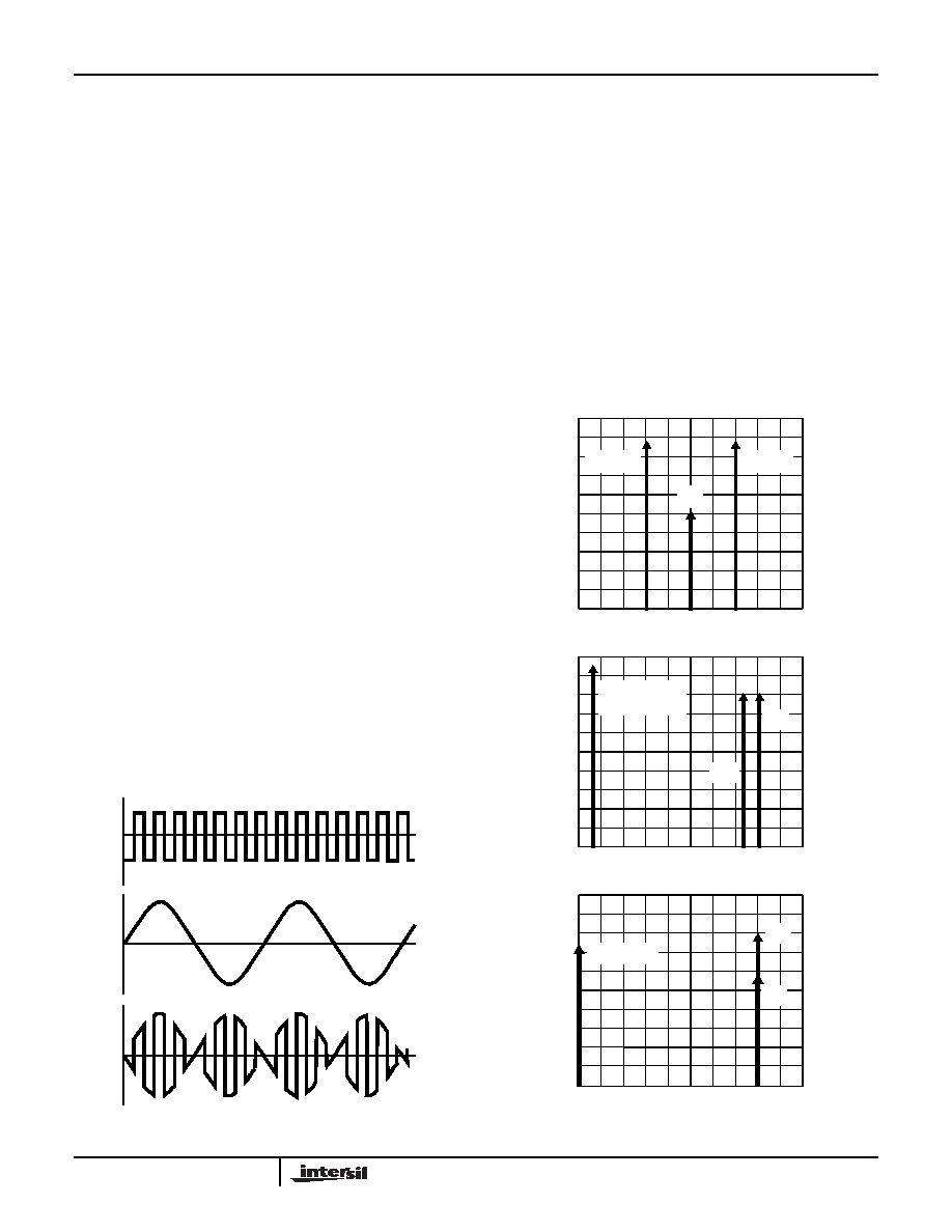
Figure 1 shows the typical input waveforms where the
frequency of the carrier is higher than the modulating signal.
The output waveform shows a typical suppressed carrier
output of an up converter or an AM signal generator.
Carrier suppression capability is a property of the well known
Balanced modulator in which the output must be zero when
one or the other input (carrier or modulating signal) is equal
to zero. however, at very high frequencies, high frequency
mismatches and AC offsets are always present and the
suppression capability is often degraded causing carrier and
modulating feedthrough to be present.
Being a frequency translation circuit, the balanced modulator
has the properties of translating the modulating frequency
(
M
) to the carrier frequency (
C
), generating the two side
bands
U
=
C
+
M
and
L
=
C
-
M
. Figure 2 shows
some translating schemes being used by
balanced mixers.
CARRIER SIGNAL
MODULATING SIGNAL
DIFFERENTIAL OUTPUT
+1
-1
FIGURE 1. TYPICAL MODULATOR SIGNALS
FIGURE 2A. UP CONVERSION OR SUPPRESSED CARRIER AM
FIGURE 2B. DOWN CONVERSION
FIGURE 2C. ZERO IF OR DIRECT DOWN CONVERSION
FIGURE 2. MODULATOR FREQUENCY SPECTRUM
C
+
M
C
-
M
C
IF
(
C -
M)
FOLDED BACK
M
C
BASEBAND
C
M
HFA3101