 | –≠–ª–µ–∫—Ç—Ä–æ–Ω–Ω—ã–π –∫–æ–º–ø–æ–Ω–µ–Ω—Ç: HFA3127MJ | –°–∫–∞—á–∞—Ç—å:  PDF PDF  ZIP ZIP |
1
CAUTION: These devices are sensitive to electrostatic discharge; follow proper IC Handling Procedures.
1-888-INTERSIL or 321-724-7143 | Copyright © Intersil Corporation 1999
HFA3127/883
Ultra High Frequency Transistor Array
Description
The HFA3127/883 is an Ultra High Frequency Transistor
Array fabricated on the Intersil Corporation complementary
bipolar UHF-1 process. This array consists of five dielectri-
cally isolated transistors on a common monolithic substrate.
The high f
T
(8GHz) and low noise figure (3.5dB) of these
transistors make them ideal for high frequency amplifier and
mixer applications.
The HFA3127/883 is an all-NPN array. Access is provided to
each of the terminals of the individual transistors for maxi-
mum application flexibility. The monolithic construction of the
array provides close electrical and thermal matching of the
five transistors.
SMD 5962-9474901MEA version is also available from Inter-
sil Corporation.
Ordering Information
PART NUMBER
TEMPERATURE
PACKAGE
HFA3127MJ/883
-55
o
C to +125
o
C
16 Lead CerDIP
Features
∑ This Circuit is Processed in Accordance to MIL-STD-
883 and is Fully Conformant Under the Provisions of
Paragraph 1.2.1.
∑ NPN Transistor (f
T
). . . . . . . . . . . . . . . . . . . . .8GHz (Typ)
∑ NPN Current Gain . . . . . . . . . . . . . . . . . . . . . . . 40 (Min)
∑ NPN Early Voltage (VA) . . . . . . . . . . . . . . . . . . . 20 (Min)
∑ Noise Figure (50
) at 1.0GHz . . . . . . . . . . . 3.5dB (Typ)
∑ Collector-to-Collector Leakage. . . . . . . . . . . <1pA (Typ)
∑ Complete Isolation Between Transistors
∑ Pin Compatible with Industry Standard 3XXX Series
Applications
∑ VHF/UHF Amplifiers
∑ VHF/UHF Mixers
∑ IF Converters
∑ Synchronous Detectors
February 1995
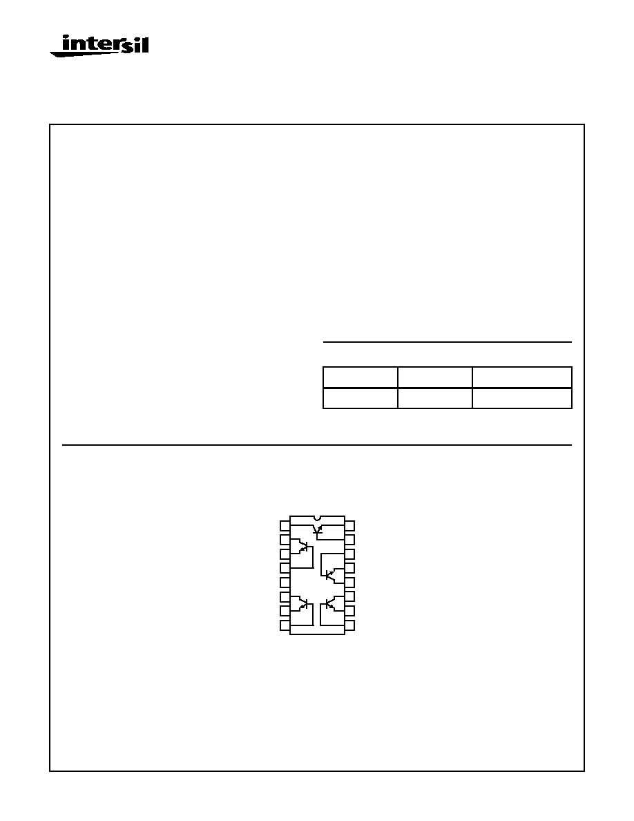
Pinout
HFA3127/883
(CERDIP)
TOP VIEW
14
15
16
9
13
12
11
10
1
2
3
4
5
7
6
8
Q1
Q2
Q3
Q4
NC
Q5
File Number
3967
Spec Number
511120
2
Specifications HFA3127/883
Absolute Maximum Ratings
Thermal Information
Collector to Emitter Voltage . . . . . . . . . . . . . . . . . . . . . . . . . . . . 8.0V
Collector to Base Voltage . . . . . . . . . . . . . . . . . . . . . . . . . . . . . 12.0V
Emitter to Base Voltage . . . . . . . . . . . . . . . . . . . . . . . . . . . . . . . 5.5V
Collector Current at 100% Duty Cycle, 175
o
C T
J
. . . . . . . . . 11.3mA
Storage Temperature Range . . . . . . . . . . . . . . . . . . -65
o
C to 150
o
C
Junction Temperature (DIE) . . . . . . . . . . . . . . . . . . . . . . . . . +175
o
C
Lead Temperature (Soldering 10s) . . . . . . . . . . . . . . . . . . . . +300
o
C
ESD Rating. . . . . . . . . . . . . . . . . . . . . . . . . . . . . . . . . . . . . . <2000V
Thermal Resistance
JA
JC
CerDIP Package . . . . . . . . . . . . . . . . . . . 80
o
C/W 24
o
C/W
Maximum Package Power Dissipation at +75
o
CerDIP Package . . . . . . . . . . . . . . . . . . . . . . . . . . . . . . . . . 1.25W
Derating Factor Above +75
o
C
CerDIP Package . . . . . . . . . . . . . . . . . . . . . . . . . . . . .12.5mW/
o
C
CAUTION: Stresses above those listed in "Absolute Maximum Ratings" may cause permanent damage to the device. This is a stress only rating and operation
of the device at these or any other conditions above those indicated in the operational sections of this specification is not implied.
Operating Conditions
Operating Temperature Range . . . . . . . . . . . . . . . . -55
o
C to +125
o
C
TABLE 1. DC ELECTRICAL PERFORMANCE CHARACTERISTICS
PARAMETER
SYMBOL
CONDITIONS
GROUP A
SUBGROUPS
TEMPERATURE
LIMITS
UNITS
MIN
MAX
Collector-to-Base
Breakdown Voltage
V
(BR)CBO
I
C
= 100
µ
A, I
E
= 0
1
+25
o
C
12
-
V
2, 3
+125
o
C to -55
o
C
12
-
V
Collector-to-Emitter
Breakdown Voltage
V
(BR)CEO
I
C
= 100
µ
A, I
B
= 0
1
+25
o
C
8
-
V
2, 3
+125
o
C to -55
o
C
8
-
V
Collector-to-Emitter
Breakdown Voltage
V
(BR)CES
I
C
= 100
µ
A, Base Shorted
tp Emitter
1
+25
o
C
10
-
V
2, 3
+125
o
C to -55
o
C
10
-
V
Emitter-to-Base Breakdown
Voltage
V
(BR)EBO
I
E
= 10
µ
A, I
C
= 0
1
+25
o
C
5.5
-
V
2, 3
+125
o
C to -55
o
C
5.5
-
V
Collector-Cutoff Current
I
CEO
V
CE
= 6V, I
B
= 0
1
+25
o
C
-
100
nA
2, 3
+125
o
C to -55
o
C
-
100
nA
Collector-Cutoff Current
I
CBO
V
CB
= 8V, I
E
= 0
1
+25
o
C
-
10
nA
2, 3
+125
o
C to -55
o
C
-
10
nA
Collector-to-Emitter
Saturation Voltage
V
CE(SAT)
I
C
= 10mA, I
B
= 1mA
1
+25
o
C
-
0.5
V
2, 3
+125
o
C to -55
o
C
-
0.5
V
Base-to-Emitter Voltage
V
BE
I
C
= 10mA
1
+25
o
C
-
0.95
V
2, 3
+125
o
C to -55
o
C
-
1.05
V
DC Forward Current
Transfer Ratio
h
FE
I
C
= 10mA, V
CE
= 2V
1
+25
o
C
40
-
-
2, 3
+125
o
C to -55
o
C
20
-
-
Early Voltage
V
A
I
C
= 10mA, V
CE
= 3.5V
1
+25
o
C
20
-
V
2, 3
+125
o
C to -55
o
C
20
-
V
Spec Number
511120
3
Specifications HFA3127/883
TABLE 2. ELECTRICAL PERFORMANCE CHARACTERISTICS
Table 2 Intentionally Left Blank.
TABLE 3. ELECTRICAL PERFORMANCE CHARACTERISTICS
Table 3 Intentionally Left Blank.
TABLE 4. ELECTRICAL TEST REQUIREMENTS
MIL-STD-883 TEST REQUIREMENTS
SUBGROUPS (SEE TABLE 1)
Interim Electrical Parameters (Pre Burn-In)
1
Final Electrical Test Parameters
1 (Note 1), 2, 3
Group A Test Requirements
1, 2, 3
Groups C and D Endpoints
1
NOTE:
1. PDA applies to Subgroup 1 only.
Spec Number
511120
4
HFA3127/883
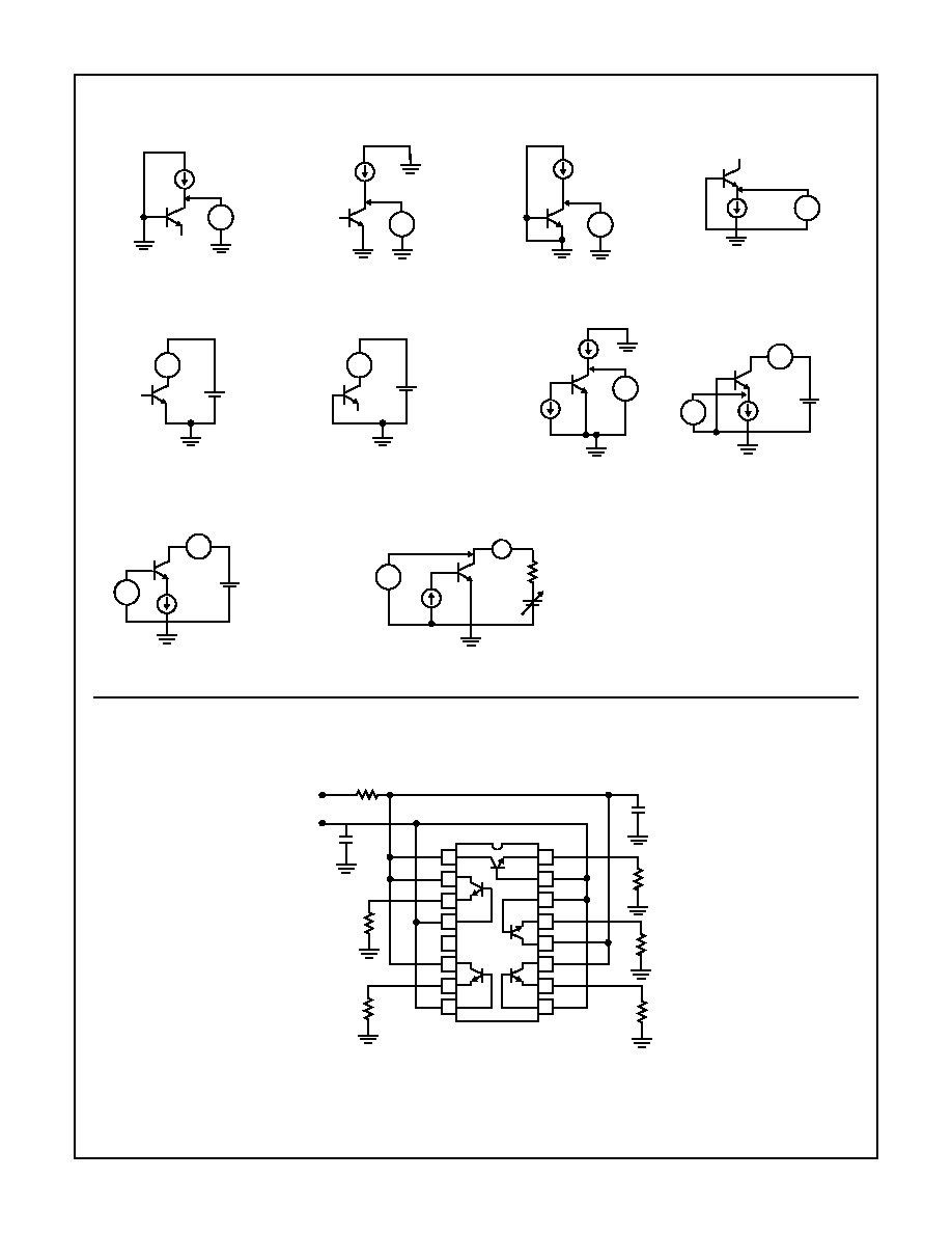
Test Circuits
(Applies to Table 1)
BVCBO
BVCEO
BVCES
BVEBO
ICEO
ICBO
VCE(SAT)
VBE
HFE
VA
Burn-In Circuit
V
100
µ
A
V
100
µ
A
V
100
µ
A
V
10
µ
A
A
6V
A
8V
V
10mA
1mA
V
A
READ 10mA
ADJ.
2V
A
READ 10mA
ADJ.
2V
A
MONITOR
ADJ.
V
R
MONITOR
ADJUST
A
14
15
16
9
13
12
11
10
1
2
3
4
5
7
6
8
Q1
Q2
Q3
Q4
NC
1K
±
5%
1K
±
5%
1K
±
5%
1K
±
5%
1K
±
5%
0.01
µ
F
100
±
5%
10.5V
±
0.5V
5.5V
±
0.5V
0.01
µ
F
Q5
Spec Number
511120
5
HFA3127/883
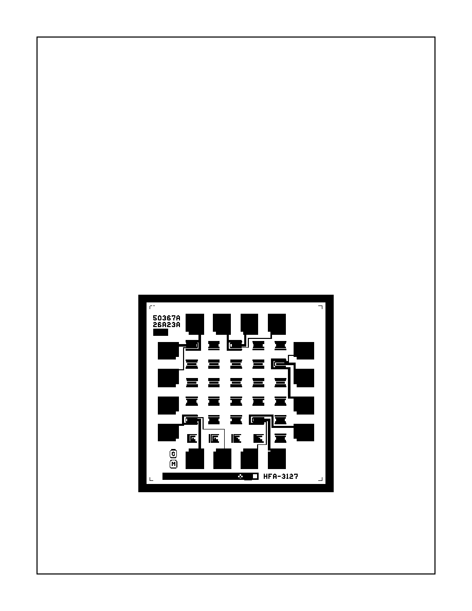
Die Characteristics
DIE DIMENSIONS:
52 x 52.8 x 15 1mils
1320
µ
m x 1340
µ
m x 381
µ
m
±
25.4
µ
m
METALIZATION:
Type: Metal 1: AlCu(2%)/TiW
Thickness: Metal 1: 8k
≈
±
0.5k
≈
Type: Metal 2: AlCu(2%)
Thickness: Metal 2: 16k
≈
±
0.8k
≈
GLASSIVATION:
Type: Nitride
Thickness: 4k
≈
±
0.5k
≈
WORST CASE CURRENT DENSITY:
3.04 x 10
5
A/cm
2
TRANSISTOR COUNT:
5
SUBSTRATE POTENTIAL:
Floating
Metallization Mask Layout
Pad numbers correspond to the 16 pin DIP pinout.
HFA3127/883
1
2
3
4
5
6
7
8
9
10
11
12
13
14
15
16
Spec Number
511120