 | –≠–ª–µ–∫—Ç—Ä–æ–Ω–Ω—ã–π –∫–æ–º–ø–æ–Ω–µ–Ω—Ç: HFA3421IB | –°–∫–∞—á–∞—Ç—å:  PDF PDF  ZIP ZIP |

2-1
TM
File Number
4288.1
CAUTION: These devices are sensitive to electrostatic discharge; follow proper IC Handling Procedures.
1-888-INTERSIL or 321-724-7143
|
Intersil and Design is a trademark of Intersil Corporation.
|
Copyright
©
Intersil Corporation 2000
PRISMÆ is a registered trademark of Intersil Corporation. PRISM logo is a trademark of Intersil Corporation.
HFA3421
1.7GHz - 2.3GHz Low Noise Amplifier
The Intersil HFA3421 PRISMÆ is a high
performance low noise amplifier in a
low cost SOIC 8 lead surface mount
plastic package. The HFA3421 employs
a fully monolithic design which
eliminates the need for external tuning networks. It can be
biased using 3V or 5V supplies and has an option for biasing
at higher currents for increased dynamic range.
The HFA3421 is ideally suited for use where low noise
figure, high gain, high dynamic range and low power
consumption are required. Typical applications include
receiver front ends in the Wireless Local Loop (WLL)
systems, as well as standard gain blocks, buffer amps, driver
amps and IF amps in both fixed and portable systems.
Pinout
HFA3421
(SOIC)
TOP VIEW
Features
∑ Low Noise Figure . . . . . . . . . . . . . . . . . . . . . . . . . . 1.65dB
∑ High Gain . . . . . . . . . . . . . . . . . . . . . . . . . . . . . . . . . .20dB
∑ Low Power Consumption . . . . . . . . . . . . . . 3V to 5V, 8mA
∑ High Dynamic Range
∑ DC Decoupled RF Input and Output
∑ No External RF Tuning Elements Necessary
∑ Low Cost SOIC 8 Lead Plastic Package
Applications
∑ Wireless Local Loop
∑ TDD Quadrature-Modulated Communication Systems
∑ Wireless Local Area Networks
∑ PCMCIA Wireless Transceivers
∑ TDMA Packet Protocol Radio
∑ PCS/Wireless PBX
Functional Block Diagram
Ordering Information
PART NUMBER
TEMP.
RANGE (
o
C)
PACKAGE
PKG.
NO.
HFA3421IB
-40 to 85
8 Ld SOIC
M8.15
HFA3421IB96
-40 to 85
Tape and Reel
GND
V
BIAS
RF IN
GND
1
2
3
4
8
7
6
5
GND
V
DD
RF OUT
GND
V
DD
RF IN
LNA 1
RF OUT
EXTENDED
BIAS
Data Sheet
September 1997
2-2
Absolute Maximum Ratings
Thermal Information
Supply Voltage, V
DD
. . . . . . . . . . . . . . . . . . . . . . . . . . . . . . +10V
DC
Input Power . . . . . . . . . . . . . . . . . . . . . . . . . . . . . . . . . . . . . +17dBm
Supply Current (Note 1) . . . . . . . . . . . . . . . . . . . . . . . . . . . . . . 30mA
Operating Conditions
Temperature Range . . . . . . . . . . . . . . . . . . . . . . . . . . -40
o
C to 85
o
C
Thermal Resistance (Typical, Note 2)
JA
(
o
C/W)
SOIC Package . . . . . . . . . . . . . . . . . . . . . . . . . . . . .
165
Maximum Storage Temperature Range . . . . . . . . . . -65
o
C to 150
o
C
Maximum Lead Temperature (Solder 10s). . . . . . . . . . . . . . . .300
o
C
(SOIC - Lead Tips Only)
CAUTION: Stresses above those listed in "Absolute Maximum Ratings" may cause permanent damage to the device. This is a stress only rating and operation of the
device at these or any other conditions above those indicated in the operational sections of this specification is not implied.
NOTES:
1. Only if pin #2 is used to increase current.
2.
JA
is measured with the component mounted on an evaluation PC board in free air.
Electrical Specifications
T
A
= 25
o
C, Z
0
= 50
, V
DD
= +5V, P
IN
= -30dBm, f = 1.7-2.3GHz, V
BIAS
= Open Circuit
Unless Otherwise Specified
PARAMETER
MIN
TYP
MAX
UNITS
LNA Input Frequency Range
1.7
-
2.3
GHz
Gain
14
20
dB
Noise Figure
-
1.65
2.30
dB
Input VSWR
-
1.5:1
-
Output VSWR
-
1.5:1
-
Input Return Loss
-
-14.0
-
dB
Output Return Loss
-
-14.0
-
dB
Output 1dB Compression
-
7
-
dBm
Input IP
3
-
-1
-
dBm
Reverse Isolation
-
30
-
dB
Supply Current at V
CC
= 5V
-
8
-
mA
Supply Range
2.7
-
5.5
V
V
BIAS
Voltage
TBD
TBD
TBD
V
V
BIAS
Current
TBD
TBD
TBD
mA
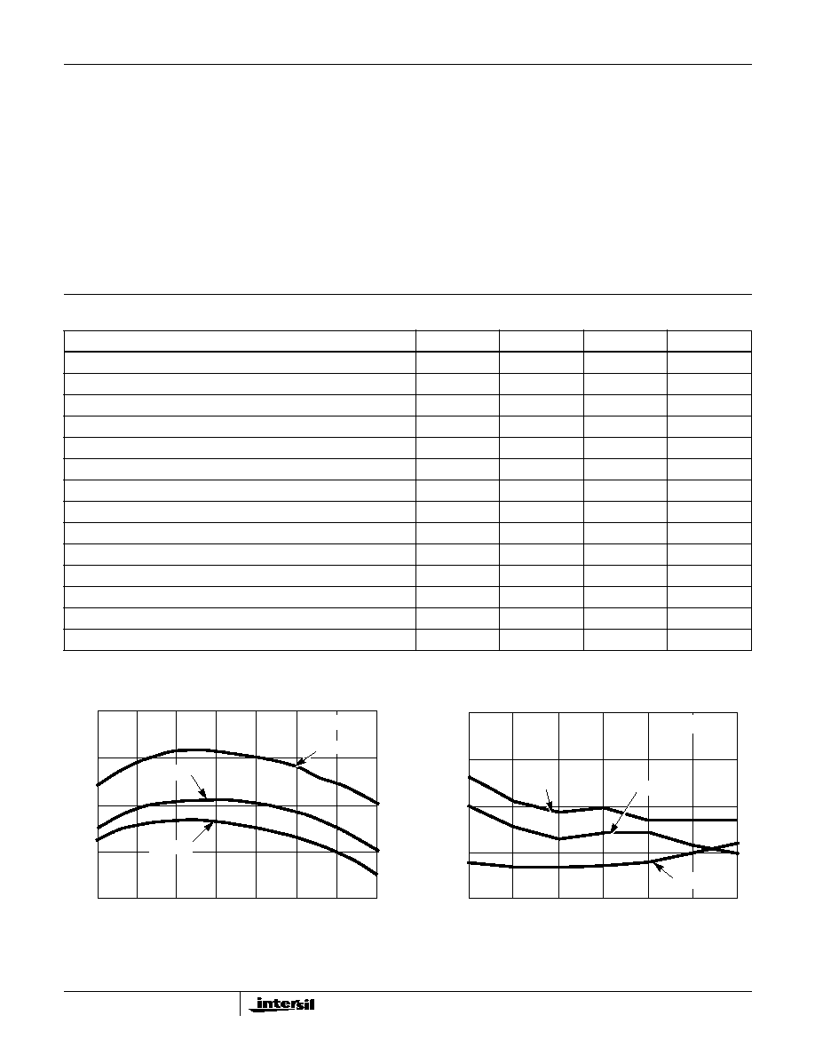
Typical Performance Curves
FIGURE 1. GAIN vs FREQUENCY
FIGURE 2. NOISE FIGURE vs FREQUENCY
24
22
20
18
16
1.5
1.6
1.7
1.8
1.9
2.0
2.1
2.2
FREQUENCY (GHz)
GAIN (dB)
T
A
= 25
o
C
5V, 20mA
5V, 8mA
3V, 8mA
1.9
1.8
1.7
1.6
1.5
1.70
1.75
1.80
1.85
1.90
1.95
2.00
FREQUENCY (GHz)
NOISE FIGURE (dB)
T
A
= 25
o
C
5V, 20mA
5V, 8mA
3V, 8mA
HFA3421

2-3
Typical Application Circuit
FIGURE 3. VSWR vs FREQUENCY
FIGURE 4. INPUT IP
3
vs FREQUENCY
FIGURE 5. GAIN vs FREQUENCY
FIGURE 6. NOISE FIGURE vs FREQUENCY
Typical Performance Curves
(Continued)
3.0
2.5
2.0
1.5
1.0
1.5
1.6
1.7
1.8
1.9
2.0
2.1
2.2
FREQUENCY (GHz)
VSWR
T
A
= 25
o
C
5V, 8mA
INPUT
OUTPUT
2
0
-4
-8
1.70
1.75
1.80
1.85
1.90
1.95
2.00
FREQUENCY (GHz)
INPUT IP
3
(dBm)
T
A
= 25
o
C
-2
-6
5V, 20mA
5V, 8mA
3V, 8mA
24
22
20
18
16
1.5
1.6
1.7
1.8
1.9
2.0
2.1
2.2
FREQUENCY (GHz)
GAIN (dB)
T
A
= 25
o
C
25
o
C
85
o
C
-40
o
C
2.4
2.1
1.8
1.5
1.2
1.70
1.75
1.80
1.85
1.90
1.95
2.00
FREQUENCY (GHz)
NOISE FIGURE (dB)
5V, 8mA
25
o
C
85
o
C
-40
o
C
R
BB
1
2
3
4
8
7
6
5
+V
DD
RF SIGNAL OUTPUT
15nH
2.4GHz
500pF
RF SIGNAL INPUT
2.4GHz
PIN 2 ALLOWS FOR AN EXTERNAL RESISTOR
R
BB
TO BE USED TO GROUND FOR AN OPTIONAL
20mA CURRENT OPERATION. RECOMMENDED
VALUES FOR THE CHIP RESISTOR ARE 30
TO 35
.
V
BIAS
(PIN 2)
NORMAL BIAS
EXTENDED BIAS
Open
30
to 35
to Ground
FIGURE 7. REFERENCE APPLICATION/TEST DESIGN SETUP SCHEMATIC: LOW NOISE AMPLIFIER
HFA3421