 | –≠–ª–µ–∫—Ç—Ä–æ–Ω–Ω—ã–π –∫–æ–º–ø–æ–Ω–µ–Ω—Ç: HFA3524IA | –°–∫–∞—á–∞—Ç—å:  PDF PDF  ZIP ZIP |
TM
1
File Number
4062.8
HFA3524
2.5GHz/600MHz Dual Frequency
Synthesizer
The Intersil 2.4GHz PRISMÆ chip set is
a highly integrated six-chip solution for
RF modems employing Direct
Sequence Spread Spectrum (DSSS)
signaling. The HFA3524 600MHz Dual
Frequency Synthesizer is one of the six chips in the PRISM
chip set (see the Typical Application Diagram).
The HFA3524 is a monolithic, integrated dual frequency
synthesizer, including prescaler, is to be used as a local
oscillator for RF and first IF of a dual conversion transceiver.
The HFA3524 contains a dual modulus prescaler. A 32/33 or
64/65 prescaler can be selected for the RF synthesizer and a
8/9 or a 16/17 prescaler can be selected for the IF
synthesizer. Using a digital phase locked loop technique, the
HFA3524 can generate a very stable, low noise signal for the
RF and IF local oscillator. Serial data is transferred into the
HFA3524 via a three wire interface (Data, Enable, Clock).
Supply voltage can range from 2.7V to 5.5V. The HFA3524
features very low current consumption of 13mA at 3V.
Features
∑ 2.7V to 5.5V Operation
∑ Low Current Consumption
∑ Selectable Powerdown Mode I
CC
= 1
µ
A Typical at 3V
∑ Dual Modulus Prescaler, 32/33 or 64/65
∑ Selectable Charge Pump High Z State Mode
Applications
∑ Systems Targeting IEEE 802.11 Standard
∑ PCMCIA Wireless Transceiver
∑ Wireless Local Area Network Modems
∑ TDMA Packet Protocol Radios
∑ Part 15 Compliant Radio Links
∑ Portable Battery Powered Equipment
Functional Block Diagram
Ordering Information
PART
NUMBER
TEMP.
RANGE (
o
C)
PACKAGE
PKG. NO.
HFA3524IA
-40 to 85
20 Ld TSSOP
M20.173
HFA3524IA96
-40 to 85
Tape and Reel
IF
PRESCALER
15-BIT IF
N COUNTER
15-BIT IF
R COUNTER
15-BIT RF
R COUNTER
18-BIT RF
N COUNTER
OSC
RF
PRESCALER
CHARGE
PUMP
f
OUT
FASTLOCK
LOCK
DETECT
f
IN
IF
OSC
IN
f
IN
RF
CLOCK
DATA
LE
PHASE
COMP
D
O
IF
LD
RF
PHASE
COMP
D
O
RF
F
O
/LD
CHARGE
PUMP
22-BIT DATA
REGISTER
IF
LD
MUX
Data Sheet
March 2000
CAUTION: These devices are sensitive to electrostatic discharge; follow proper IC Handling Procedures.
1-888-INTERSIL or 321-724-7143
|
Intersil and Design is a trademark of Intersil Corporation.
|
Copyright
©
Intersil Corporation 2000
PRISMÆ is a registered trademark of Intersil Corporation. PRISM logo is a trademark of Intersil Corporation.
2
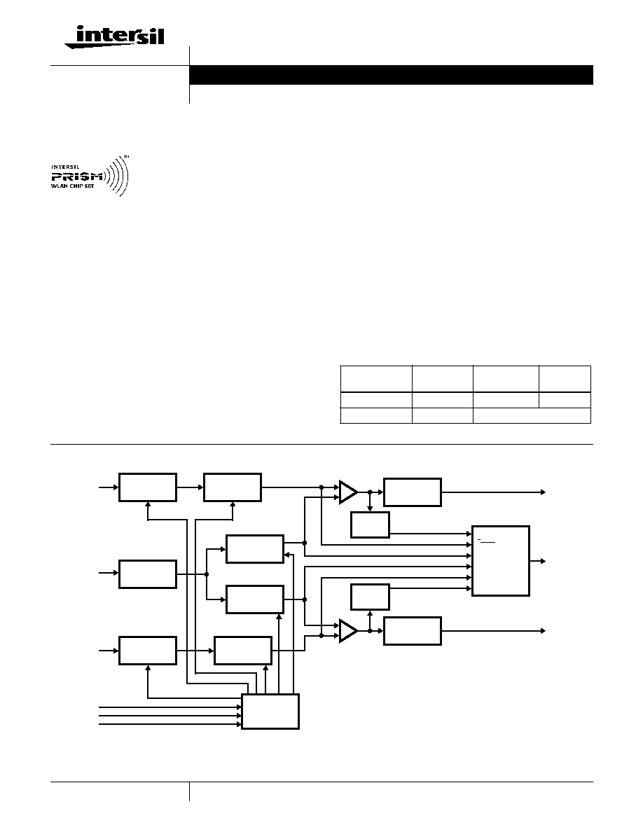
Typical Application Diagram
For additional information on the PRISM chip set, see us on
the web http://www.intersil.com/prism or call (321) 724-7800
to access Intersil' AnswerFAX system. When prompted, key
in the four-digit document number (File #) of the datasheets
you wish to receive.
The four-digit file numbers are shown in Typical Application
Diagram, and correspond to the appropriate circuit.
QUAD IF MODULATOR
RFPA
HFA3925
HFA3724
DSSS BASEBAND PROCESSOR
D
A
T
A
T
O
MA
C
CTRL
HSP3824
TUNE/SELECT
HFA3524
0
o
/90
o
VCO
A/D
A/D
MAC-PHY
INTERFACE
802.11
VCO
HFA3624
UP/DOWN
CONVERTER
A/D
(FILE# 4067)
(FILE# 4064)
(FILE# 4062)
(FILE# 4066)
(FILE# 4132)
PRISM CHIP SET FILE #4063
M
U
X
M
U
X
DPSK
DEMOD
DPSK
MOD.
DE-
SPREAD
SPREAD
Q
I
HFA3424
(NOTE)
(FILE# 4131)
NOTE: Required for systems targeting 802.11 specifications.
TYPICAL TRANSCEIVER APPLICATION CIRCUIT USING THE HFA352
CCA
RXI
RXQ
RSSI
TXI
TXQ
˜
2
DUAL SYNTHESIZER
HFA3524
3
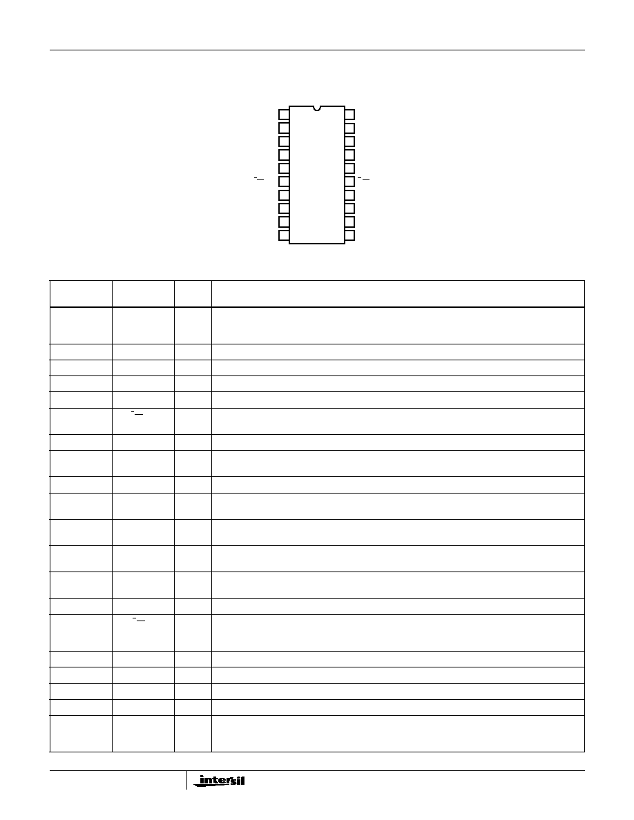
Pinout
HFA3524 (TSSOP)
TOP VIEW
Pin Descriptions
PIN
NUMBER
PIN NAME
I/O
DESCRIPTION
1
V
CC1
-
Power supply voltage input. Input may range from 2.7V to 5.5V. V
CC1
must equal V
CC2
. Bypass
capacitors should be placed as close as possible to this pin and be connected directly to the ground
plane.
2
V
P1
-
Power Supply for RF charge pump. Must be > V
CC
.
3
D
O
RF
O
Internal charge pump output. For connection to a loop filter for driving the input of an external V
CO
.
4
GND
-
Ground.
5
f
IN
RF
I
RF prescaler input. Small signal input from the V
CO
.
6
f
IN
RF
l
RF prescaler complimentary input. A bypass capacitor should be placed as close as possible to this
pin and be connected directly to the ground plane. Capacitor is optional with some loss of sensitivity.
7
GND
-
Ground.
8
OSC
IN
I
Oscillator input. The input has a V
CC
/2 input threshold and can be driven from an external CMOS
or TTL logic gate.
9
GND
-
Ground.
10
F
O
/LD
O
Multiplexed output of the RF/lF programmable or reference dividers, RF/lF lock detect signals and
Fastlock mode. CMOS output (see Programmable Modes).
11
Clock
I
High impedance CMOS Clock input. Data for the various counters is clocked in on the rising edge,
into the 22-bit shift register.
12
Data
l
Binary serial data input. Data entered MSB first. The last two bits are the control bits. High
impedance CMOS input.
13
LE
l
Load enable CMOS input. When LE goes HIGH, data stored in the shift registers is loaded into one
of the 4 appropriate latches (control bit dependent).
14
GND
-
Ground.
15
f
IN
IF
I
IF prescaler complimentary input. A bypass capacitor should be placed as close as possible to
this pin and be connected directly to the ground plane. Capacitor is optional with some loss of
sensitivity.
16
f
IN
IF
I
IF prescaler input. Small signal input from the V
CO
.
17
GND
-
Ground.
18
D
O
IF
O
IF charge pump output. For connection to a loop filter for driving the input of an external V
CO
.
19
V
P2
-
Power Supply for IF charge pump. Must be >V
CC
.
20
V
CC2
-
Power supply voltage input Input may range from 2.7V to 5.5V. V
CC2
must equal V
CC1
. Bypass
capacitors should be placed as close as possible to this pin and be connected directly to the ground
plane.
11
12
13
14
15
16
17
18
20
19
10
9
8
7
6
5
4
3
2
1
V
CC1
V
P1
D
O
RF
GND
f
IN
RF
f
IN
RF
OSC
IN
GND
GND
F
O
/LD
V
CC2
D
O
IF
GND
f
IN
IF
V
P2
f
IN
IF
GND
LE
DATA
CLOCK
HFA3524

4
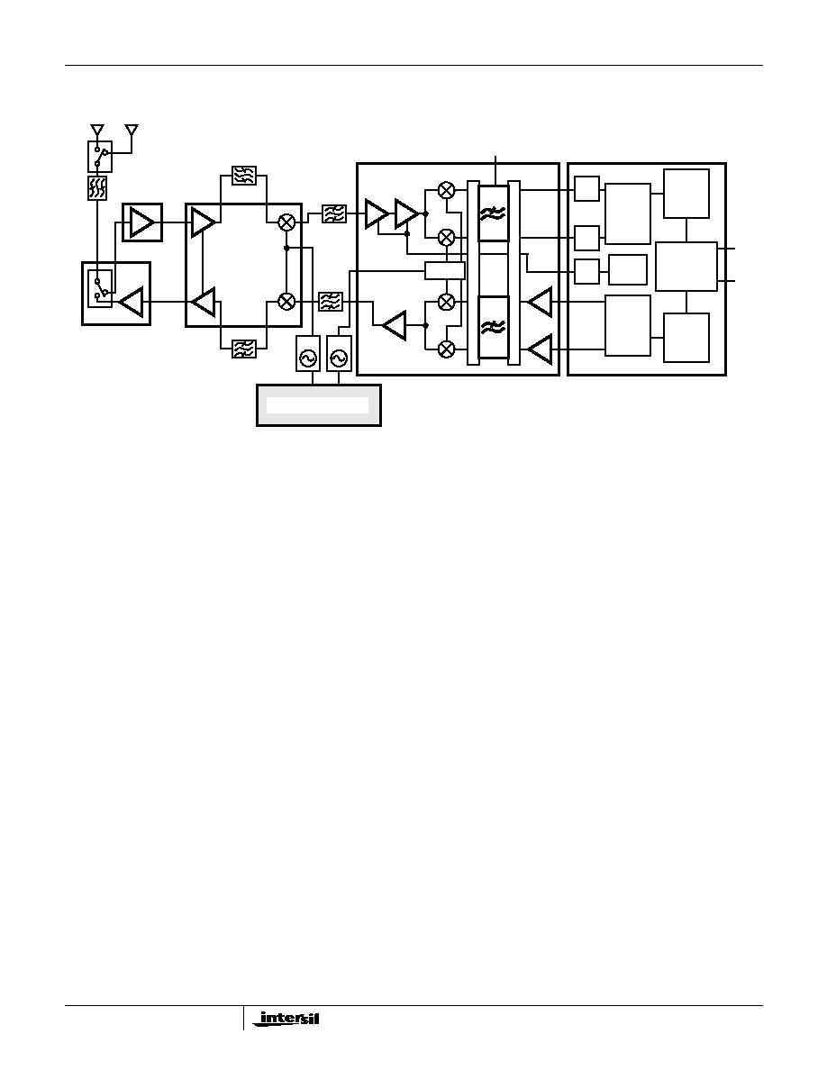
Block Diagram
LOCK DETECT/
FASTLOCK
MULTIPLEXER
f
OUT
/
LOCK
DETECT
RF
RF CHARGE PUMP
1X
4X
V
CC1
1
V
P1
2
3
GND
4
D
O
RF
RF PRESCALER
32/33 OR 64/65
CONTROL
SWALLOW
FR 1
FP 1
PHASE
DETECTOR
RF
PD
PU
+
-
f
IN
RF
5
6
GND
7
f
IN
RF
(RF) 18-BIT N-LATCH
LATCH
1-BIT P1
PWDN
1-BIT RF
15-BIT R1 LATCH
5-BIT MODE LATCH
LOCK
DETECT
IF
IF CHARGE PUMP
4X
1X
V
CC2
20
V
P2
19
18
GND
17
D
O
IF
15-BIT (IF)
N-COUNTER
PROGRAMMABLE
IF PRESCALER
8/9 OR 16/17
CONTROL
SWALLOW
FR 2
FP 2
PHASE
DETECTOR
IF
PD
PU
+
-
f
IN
IF
16
15
GND
14
f
IN
IF
(IF) 15-BIT N-LATCH
LATCH
1-BIT P2
PWDN
1-BIT IF
PROGRAMMABLE 15-BIT
(R2) REFERENCE COUNTER
OSC
IN
8
GND
9
15-BIT R2 LATCH
5-BIT MODE LATCH
10
F
O
LD
DECODE
LATCH
20-BIT SHIFT REGISTER
18-BIT (RF)
N-COUNTER
PROGRAMMABLE
PROGRAMMABLE 15-BIT
(R1) REFERENCE COUNTER
CONTROL
2-BIT
LATCH
13
LE
12
DATA
11
CLOCK
NOTES:
1. V
CC1
supplies power to the RF prescaler, N-counter and phase detector. V
CC2
supplies power to the IF prescaler, N-counter and phase detector,
RF and IF R-counters along with the OSC
IN
buffer and all digital circuitry. V
CC1
and V
CC2
are separated by a diode and must be run at the
same voltage level.
2. V
P1
and V
P2
can be run independently as long as V
P
V
CC
.
HFA3524
5
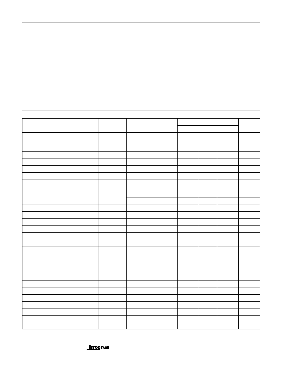
Absolute Maximum Ratings
Thermal Information
Power Supply Voltage
V
CC
. . . . . . . . . . . . . . . . . . . . . . . . . . . . . . . . . . . . -0.3V to +6.5V
V
P
. . . . . . . . . . . . . . . . . . . . . . . . . . . . . . . . . . . . . . -0.3V to +6.5V
Voltage on Any Pin with GND = 0V (V
I
) . . . . . . . . . . . -0.3V to +6.5V
Operating Conditions
Power Supply Voltage
V
CC
. . . . . . . . . . . . . . . . . . . . . . . . . . . . . . . . . . . . . . 2.7V to 5.5V
V
P
. . . . . . . . . . . . . . . . . . . . . . . . . . . . . . . . . . . . . . . . . . . .V
CC
to +5.5V
Temperature (T
A
) . . . . . . . . . . . . . . . . . . . . . . . . . . . . -40
o
C to 85
o
C
Thermal Resistance (Typical, Note 3)
JA
(
o
C/W)
TSSOP Package . . . . . . . . . . . . . . . . . . . . . . . . . . .
130
Maximum Storage Temperature Range (T
S
) . . . . . . -55
o
C to 150
o
C
Maximum Lead Temperature (Soldering 4s) (T
L
) . . . . . . . . . .260
o
C
(TSSOP - Lead Tips Only)
CAUTION: Stresses above those listed in "Absolute Maximum Ratings" may cause permanent damage to the device. This is a stress only rating and operation of the
device at these or any other conditions above those indicated in the operational sections of this specification is not implied.
NOTE:
3.
JA
is measured with the component mounted on an evaluation PC board in free air.
Electrical Specifications
V
CC
= 3.0V, V
P
= 3.0V, -40
o
C < T
A
< 85
o
C, Unless Otherwise Specified
PARAMETER
SYMBOL
TEST CONDITIONS
HFA3524
UNITS
MIN
TYP
MAX
Power Supply Current
I
CC
RF + IF
V
CC
= 2.7V to 5.5V
-
13
-
mA
RF Only
V
CC
= 2.7V to 5.5V
-
10
-
mA
Powerdown Current
I
CC-PWDN
V
CC
= 3.0V
-
1
25
µ
A
Operating Frequency
f
IN
RF
0.5
-
2.5
GHz
Operating Frequency
f
IN
IF
45
-
600
MHz
Oscillator Frequency
f
OSC
5
-
44
MHz
Maximum Phase Detector
Frequency
f
10
-
-
MHz
RF Input Sensitivity
Pf
IN
RF
V
CC
= 3.0V
-15
-
+4
dBm
V
CC
= 5.0V
-10
-
+4
dBm
IF Input Sensitivity
Pf
IN
IF
V
CC
= 2.7V to 5.5V
-10
-
+4
dBm
Oscillator Sensitivity
V
OSC
OSC
IN
0.5
-
-
V
P-P
High Level Input Voltage
V
IH
(Note)
0.8V
CC
-
-
V
Low Level Input Voltage
V
IL
(Note)
-
-
0.2V
CC
V
High Level Input Current
I
IH
V
IH
= V
CC
= 5.5V (Note)
-1.0
-
1.0
µ
A
Low Level Input Current
I
IL
V
IL
= 0V, V
CC
= 5.5V (Note)
-1.0
-
1.0
µ
A
Oscillator Input Current
I
IH
V
IH
= V
CC
= 5.5V
-
-
100
µ
A
Oscillator Input Current
I
IL
V
IL
= 0V, V
CC
= 5.5V
-100
-
-
µ
A
High Level Output Voltage
V
OH
I
OH
= -500
µ
A
V
CC
-0.4
-
-
V
High Level Output Voltage
V
OH
I
OH
= -1mA
-
-
-
V
Low Level Output Voltage
V
OL
I
OL
= 500
µ
A
-
-
0.4
V
Low Level Output Voltage
V
OL
I
OL
= 1mA
-
-
-
V
Data to Clock Set Up Time
t
CS
See Data Input Timing
50
-
-
ns
Data to Clock Hold Time
t
CH
See Data Input Timing
10
-
-
ns
Clock Pulse Width High
t
CWH
See Data Input Timing
50
-
-
ns
Clock Pulse Width Low
t
CWL
See Data Input Timing
50
-
-
ns
Clock to Load Enable Set Up Time
t
ES
See Data Input Timing
50
-
-
ns
Load Enable Pulse Width
t
EW
See Data Input Timing
50
-
-
ns
NOTE: Clock, Data and LE does not include f
IN
RF, f
IN
IF and OSC
IN
.
HFA3524