
4-1
TM
HFA3664
2.7GHz UpConverter with Gain Control
The HFA3664 UpConverter with Gain
Control is a monolithic bipolar PRISMÆ
device for up conversion applications in
the 2.3GHz to 2.7GHz range.
Manufactured in the Intersil UHF1X
process, the device consists of a double balanced mixer
followed by a variable gain power preamp. An energy saving,
TTL Compatible, power enable input provides on/off bias
current control to the mixer and amplifier. The device
requires low drive levels from the local oscillator and is
housed in a small outline 20 lead SSOP package ideally
suited for PCMCIA card applications.
Pinout
HFA3664
(SSOP)
TOP VIEW
Features
∑ RF Frequency Range . . . . . . . . . . . . . . 2.3GHz to 2.7GHz
∑ IF Operation . . . . . . . . . . . . . . . . . . . . . 10MHz to 400MHz
∑ Gain Control Range . . . . . . . . . . . . . . . . . . . . . . . . . .20dB
∑ Single Supply Operation. . . . . . . . . . . . . . . . . 2.7V to 5.5V
∑ High Output 1dB Compression. . . . . . . . . . . . . . . . . 6dBm
∑ High Power Gain . . . . . . . . . . . . . . . . . . . . . . . . . . . .18dB
∑ Power Enable/Disable Control
Applications
∑ Wireless Local Loop Systems
∑ PCMCIA Wireless Transceiver
∑ Wireless Local Area Network Modems
∑ CDMA/TDMA Packet Protocol Radios
∑ Full Duplex Transceivers
∑ Portable Battery Powered Equipment
Block Diagram
Ordering Information
PART NUMBER
TEMP.
RANGE (
o
C)
PACKAGE
PKG.
NO.
HFA3664IA
-40 to 85
20 Ld SSOP
M20.15
HFA3664IA96
-40 to 85
Tape and Reel
TX_PE
GND
IF_IN
IF_BY
TXM_RF
MIX_V
CC
AGC_CTRL
LO_BY
PRE_V
CC
3
GND
PRE_OUT
GND
BIAS_V
CC
PRE_IN
PRE_V
CC
1
GND
GND
LO_IN
GND
PRE_V
CC
2
11
12
13
14
15
16
17
18
20
19
10
9
8
7
6
5
4
3
2
1
POWER CONTROL TRUTH TABLE
STATE
TX_PE
Power Down - Energy Saving Mode
Low
Transmit Mode
High
LO_IN
IF_IN
PRE_OUT
PRE_IN
TXM_RF
AGC_CTRL
IF_BY
AGC CONTROL
BIAS
TX_PE
PRE_V
CC
3
PRE_V
CC
2
PRE_V
CC
1
BIAS_V
CC
LO_BY
Data Sheet
April 1999
File Number
4242.3
CAUTION: These devices are sensitive to electrostatic discharge; follow proper IC Handling Procedures.
1-888-INTERSIL or 321-724-7143
|
Intersil and Design is a trademark of Intersil Corporation.
|
Copyright
©
Intersil Corporation 2000
PRISMÆ is a registered trademark of Intersil Corporation. PRISM logo is a trademark of Intersil Corporation.
4-2
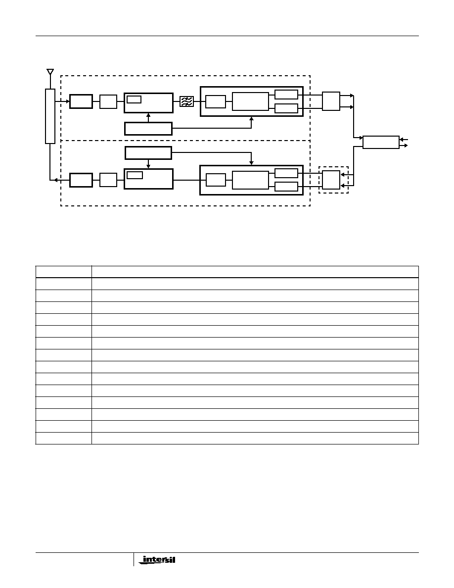
Typical Application Diagram
SYNTHESIZER
LNA
BPF
RF/IF
CONVERTER
IF AGC
LPF
QMODEM
IF/RF
CONVERTER
BASEBAND
FILTER
SYNTHESIZER
HFA3424/21
HFA3661
HFA3524
HFA3663 (File #4241)
HFA3925
HFA3761 (File #4236)
HFA3763
LPF
AGC
LPF
QMODEM
LPF
D/A
PA
BPF
HFA3664 (File #4242)
(File #4240)
(File #4062)
HFA3524
(File #4062)
(File #4132)
(File #4131)
(File #4237)
PRISM FULL DUPLEX RADIO
CHIP SET, FILE #4238
A/D
PRISM FULL DUPLEX CHIP SET
AGC
LNA
IF LO1
IF LO2
RF LO1
RF LO2
D
U
P
L
E
X
E
R
OPTIONAL WHEN IN
ANALOG MODE
Pin Descriptions
NAME
DESCRIPTION
LO_IN
Local Oscillator Input.
LO_BY
Local Oscillator Input Bypass (AC coupled to GND).
PRE_IN
Power Pre-Amplifier Input.
PRE_OUT
Power Pre-Amplifier Output.
PRE_V
CC
1
Power Pre-Amplifier 1st Stage Positive Power Supply. Use high quality RF decoupling capacitors.
PRE_V
CC
2
Power Pre-Amplifier 2nd Stage Positive Power Supply. Use high quality RF decoupling capacitors.
PRE_V
CC
3
Power Pre-Amplifier 3rd Stage Positive Power Supply. Use high quality RF decoupling capacitors.
BIAS_V
CC
LO Buffer, Bias, Mixer and AGC Control Positive Power Supply. Requires an isolation coil to V
CC
.
MIX_V
CC
Transmit Mixer Output Stage Positive Power Supply. Use high quality RF decoupling capacitors.
RX_PE
Power Enable Control Input. Refer to the Power Control Truth Table.
TXM_RF
Transmit Mixer RF Output.
IF_IN
Transmit Mixer Positive IF Input. Requires external bias resistor to V
CC
.
IF_BY
Transmit Mixer Negative IF Input (AC coupled to GND).
GND
Circuit Ground Pins (Qty 6). Internally connected with the exception of pin 17.
HFA3664
4-3
Absolute Maximum Ratings
Thermal Information
Supply Voltage . . . . . . . . . . . . . . . . . . . . . . . . . . . . . . . . -0.3 to 6.0V
Voltage on Any Other Pin. . . . . . . . . . . . . . . . . . . . -0.3 to V
CC
0.3V
Operating Conditions
Supply Voltage Range . . . . . . . . . . . . . . . . . . . . . . . . . . 2.7V to 5.5V
Thermal Resistance (Typical, Note 1)
JA
(
o
C/W)
20 Lead SSOP . . . . . . . . . . . . . . . . . . . . . . . . . . . . .
110
Package Power Dissipation at 70
o
C
20 Lead SSOP . . . . . . . . . . . . . . . . . . . . . . . . . . . . . . . . . . . .0.7W
Maximum Junction Temperature (Plastic Package) . . . . . . . . .150
o
C
Maximum Temperature Range. . . . . . . . . . . . . . . -40
o
C
T
A
85
o
C
Maximum Storage Temperature Range . . . . . . . -65
o
C
T
A
150
o
C
Maximum Lead Temperature (Soldering 10s) . . . . . . . . . . . . 300
o
C
(Lead Tips Only)
CAUTION: Stresses above those listed in "Absolute Maximum Ratings" may cause permanent damage to the device. This is a stress only rating and operation of the
device at these or any other conditions above those indicated in the operational sections of this specification is not implied.
NOTE:
1.
JA
is measured with the component mounted on an evaluation PC board in free air.
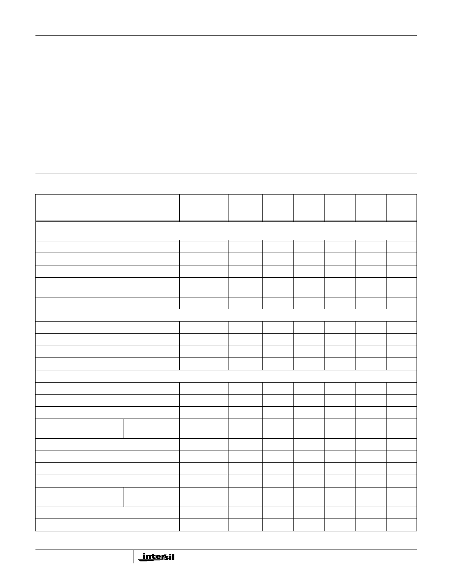
Electrical Specifications
V
CC
= 5.5V, LO = 2400MHz, IF = 100MHz, RF = 2500MHz, Z
O
= 50W,
Unless Otherwise Specified
PARAMETER
SYMBOL
(NOTE 2)
TEST
LEVEL
TEMP
(
o
C)
MIN
TYP
MAX
UNITS
CASCADED CHARACTERISTICS
(-3dB Loss RF Image Filter with 35dB LO Suppression,
LO_IN = 2400MHz/-6dBm, IF_IN = 100MHz/-30dBm, AGC_CTRL = 0.7V (Max Gain))
Cascaded Output 1dB Compression
CTX_P1D
B
25
6
7.5
-
dBm
Cascaded Output Third Order Intercept
CTX_IP3
C
25
-
14
-
dBm
Cascaded Power Gain
CTX_PG
B
25
18
23
-
dB
Cascaded Power Gain Flatness
(2.3GHz to 2.7GHz)
CTX_PGF
C
25
-2.5
0
+2.5
dB
Cascaded LO Leakage
CTX_LEAK
B
25
-
-23.8
-
dBm
LO INPUT CHARACTERISTICS (LO_IN = 2400MHz/-6dBm, all unused inputs and outputs are terminated into 50
)
LO Input Frequency Range
LO_f
B
25
1.9
-
2.29
GHz
LO Input Drive Level
LO_dr
A
25, 85
-
-6
-
dBm
LO Input VSWR
LO_SWR
A
25, 85
1.0:1
1.62:1
2.3:1
-
LO Input Return Loss
LO_IRL
A
25, 85
8.09
12.5
-
dB
TRANSMIT MIXER CHARACTERISTICS (LO_IN = 2400MHz/-6dBm, TXM_IF = 100MHz/-30dBm)
IF Input Frequency Range
TXM_IFf
B
25, 85
10
-
400
MHz
IF Input VSWR
TXM_SWR
A
25, 85
-
1.22:1
2.0:1
-
IF Input Return Loss
TXM_IRL
A
25, 85
9.5
20
-
dB
Power Conversion Gain
(Note 3)
V
CC
= 5.5V
TXM_PGH
A
25, 85
3.0
4.5
TBD
dB
Transmit Mixer LO Leakage
TXM_LEAK
A
25, 85
-
-20
-10
dBm
RF Output Frequency Range
TXM_RFf
B
25, 85
2.4
-
2.7
GHz
RF Output VSWR
TXM_OSWR
A
25, 85
1.01
1.68:1
2.3:1
-
RF Output Return Loss
TXM_ORL
A
25, 85
8.09
12
-
dB
RF Output 1dB Compression
(Note 3)
V
CC
= 5.5V
TXM_P1DH
A
25, 85
-10
-7.5
-
dBm
RF Output Third Order Intercept
TXM_IP3
C
25
-
-1.0
-
dBm
Transmit Mixer Noise Figure
TXM_NF
B
25
-
18
-
dB
HFA3664

4-4
TRANSMIT POWER PREAMP CHARACTERISTICS (PRE_IN = 2400MHz/-30dBm, AGC_CTRL = 0.7V (Max Gain))
Frequency Range
PRE_f
B
25
2.3
-
2.7
GHz
Power Gain
(AGC_CTRL = 0.7V)
V
CC
= 5.5V
PRE_PGH
A
25, 85
21
24
27
dB
Pre-Amp Noise Figure (Max Gain)
PRE_NF
B
25
-
8
-
dB
Pre-Amp AGC Range (Max - Min Gain)
PRE_AGC
A
25, 85
20
30
-
dB
AGC Control Voltage Range
AGC_V
A
25, 85
0.7
-
1.7
V
AGC Control Linearity
AGC_LIN
B
25
-
5:1
-
-
AGC Settling Time (Min to Max Gain)
AGC_T1
B
25
-
8.0
-
µ
S
AGC Settling Time (Max to Min Gain)
AGC_T2
B
25
-
0.1
-
µ
S
Pre-Amp RF Output 1dB
Compression
V
CC
= 5.5V
PRE_P1DH
A
25, 85
6
8
-
dBm
RF Output Third Order Intercept
PRE_IP3
C
25
-
14
-
dBm
Input VSWR
PRE_ISWR
A
25, 85
1.0:1
2.0:1
3.0:1
-
Input Return Loss
PRE_IRL
A
25, 85
6
7
-
dB
Output VSWR
PRE_OSWR
A
25, 85
1.0:1
1.28:1
2.3:1
-
Output Return Loss
PRE_ORL
A
25, 85
8.09
20
-
dB
POWER SUPPLY AND LOGIC CHARACTERISTICS
Voltage Supply Range
V
CC
A
25, 85
-
5.5
-
V
Supply Current (V
CC
= 5.5V)
I
CC HI
A
25, 85
90
103
110
mA
I
CC HI
T
C
Full
-
-
110
mA
Power Down Supply Current (V
CC
= 5.5V)
I
CC
_PD
A
25, 85
2
3.3
4
mA
Logic Input Low Level
V
IL
A
25, 85
-0.2
-
0.8
V
Logic Input High Level
V
IH
A
25, 85
2.0
-
V
CC
V
Logic Low Input Bias Current
(V
PE
= 0V, V
CC
= 5.5V)
I
B
_LO
A
25, 85
-5
-0.1
5
µ
A
Logic High Input Bias Current
(V
PE
= 5.5V, V
CC
= 5.5V)
I
B
_HI
A
25, 85
-5
0.6
5
µ
A
Vagc High Input Bias Current
(Vagc = 2.1V, V
CC
= 5.5V)
Ivagc_HI
A
25, 85
10
200
400
µ
A
Vagc Low Input Bias Current
(Vagc = 0.7V, V
CC
= 5.5V)
Ivagc_LO
A
25, 85
-400
-235
-10
µ
A
Power Enable Time (50% V
PE
to 90% I
CC)
PEt
B
25
-
5
10
µ
s
Power Disable Time (50% V
PE
to 10% I
CC
)
PDt
B
25
-
0.1
10
µ
s
NOTES:
2. Test Level: A = 100% production tested, B = Typical or Limit based on characterization data, C = Design information, goal or condition.
3. Bias Resistor at pin 16 changes according to the relationship mentioned in Note 4 of the Typical Applications Circuit.
Electrical Specifications
V
CC
= 5.5V, LO = 2400MHz, IF = 100MHz, RF = 2500MHz, Z
O
= 50W,
Unless Otherwise Specified (Continued)
PARAMETER
SYMBOL
(NOTE 2)
TEST
LEVEL
TEMP
(
o
C)
MIN
TYP
MAX
UNITS
HFA3664
4-5
Typical Application Circuit
20
19
18
17
16
15
14
13
12
11
1
2
3
4
5
6
7
8
9
10
TX_PE
LO_IN
LO_BY
GND
GND
MIX_V
CC
AGC_CTRL
IF_BY
PRE_V
CC
3
GND
PRE_OUT
GND
PRE_V
CC
2
PRE_IN
PRE_V
CC
1
GND
GND
IF_IN
TXM_RF
BIAS_V
CC
V
CC
= 5.0V
C5
22pF
C3
330pF
TRANSMIT
ENABLE
C1
2.2
µ
F
C2
3300pF
C8
330pF
C14
7pF
C11
RF OUTPUT
50
C9
7pF
C10
7pF
LO INPUT
50
IF INPUT
50
C12
3300pF
AGC
CONTROL
C15
3300pF
3300pF
C13
7pF
C7
7pF
AGC CONTROL
C4
7pF
50
BPF
LO REJECT
FILTER
7pF
7pF
7pF
330pF
330pF
4.7nH
NOTE 5
1.69K
NOTE
NOTE 5
NOTES:
4. Required external resistor for Mixer biasing. Value optimized for 2.7mA bias current with R = (V
CC
- 0.93) /2.7mA. Most Mixer cell characteristics
like Gain, NF etc., can be affected when biasing is outside the optimum value.
5. The combination of these attenuator pads and the Band Pass Filter insertion loss shall bring the overall Cascaded Gain at the desired frequency
of operation from 21dB to 22dB for best performance. The selection of these values is optional. The total gain, LO feedthru, Mixer and Pre-
amplifier interaction (stability) and output compression point performances can be manipulated according to the user needs.
4
HFA3664