 | –≠–ª–µ–∫—Ç—Ä–æ–Ω–Ω—ã–π –∫–æ–º–ø–æ–Ω–µ–Ω—Ç: HFA3665 | –°–∫–∞—á–∞—Ç—å:  PDF PDF  ZIP ZIP |
1
TM
PRELIMINARY
May 1999
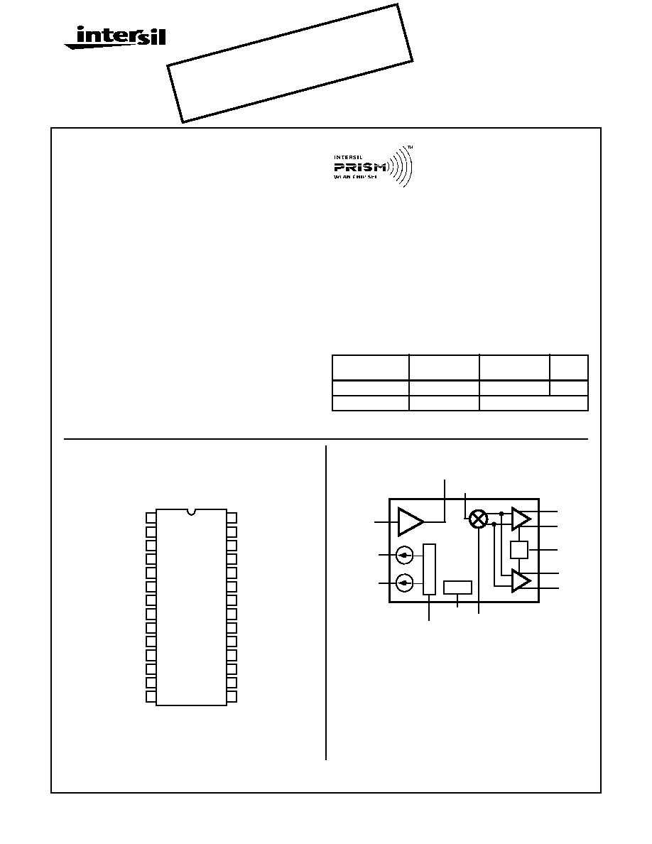
HFA3665
CDMA/AMPS Downconverter with AGC Capability
Features
∑ RF Frequency Range . . . . . . . . . . . . 869MHz to 895MHz
∑ IF Operation . . . . . . . . . . . . . . . . . . . . 10MHz to 100MHz
∑ LNA Gain. . . . . . . . . . . . . . . . . . . . . . . . . . . . . . . . . .16dB
∑ LNA NF . . . . . . . . . . . . . . . . . . . . . . . . . . . . . . . . . . 2.3dB
∑ Mixer Gain. . . . . . . . . . . . . . . . . . . . . . . . . . . . . . . . .16dB
∑ Mixer NF . . . . . . . . . . . . . . . . . . . . . . . . . . . . . . . . . .11dB
∑ Single Supply Battery Operation . . . . . . . . 2.7V to 3.3V
∑ Power Enable/Disable Control
∑ PIN Diode Attenuator DC Control
Applications
∑ IS95A CDMA/AMPS Dual Mode Handsets
∑ Wideband CDMA Handsets
∑ CDMA/TDMA Packet Protocol Radios
∑ Full Duplex Transceivers
∑ Portable Battery Powered Equipment
Description
The HFA3665 is a monolithic bipo-
lar downconverter for CDMA/AMPS
cellular applications. Manufactured
in the Intersil UHF1X process, the
device consists of a low noise cascode amplifier, a double
balanced downconversion mixer and a pair of linearized and
temperature
compensated
PIN
diode
biasing
current
sources for external RF AGC applications. In addition, the
device offers two independent and selectable differential
mixer IF output ports to be used with dual mode IF filters and
requires low drive levels from the local oscillator. The
HFA3665 is one of the four chips in the PRISMTM chip set
and is housed in a small outline 28 lead SSOP package ide-
ally suited for cellular handset applications.
PRISMTM and the PRISMTM logo are trademarks of Intersil Corporation.
Ordering Information
PART NUMBER
TEMP.
RANGE (
o
C)
PACKAGE
PKG.
NO.
HFA3665IA
-40 to 85
28 Ld SSOP
M28.15
HFA3665IA96
-40 to 85
Tape and Reel
Pinout
HFA3665
(SSOP)
TOP VIEW
Block Diagram
V
CC
GND
AGC_CTRL
PIN_O_IBIAS1
GND
LNA_OUT
LNA_OUT
GND
LNA_IN
PIN_O_IBIAS2
PIN_I_GND
RX_PE
BIAS_GND
MIX_V
CC
MIX_V
CC
RF_IN
MIX_IND
MIX_GND
LO_RET
CDMA_OUT-
CDMA_OUT+
FM_OUT-
BIAS_V
CC
SEL
RF_RET
LO_IN
28
27
26
25
24
23
22
21
20
19
18
17
16
15
1
2
3
4
5
6
7
8
9
10
11
12
13
14
R_REF
FM_OUT+
RX_PE
C
T
R
L
BIAS
SW
LNA
AGC_CTRL
LNA_OUT
LNA_IN
CDMA_OUT-
CDMA_OUT+
FM_OUT-
LO_IN
FM_OUT+
SEL
PIN_O_IBIAS2
PIN_O_IBIAS1
RF_IN
CAUTION: These devices are sensitive to electrostatic discharge. Users should follow proper IC Handling Procedures.
Copyright
©
Intersil Corporation 1999
File Number
4301.5
OBSOLETE PR
ODUCT
NO RECOMMENDED REPLA
CEMENT
Call Central Applications 1-800-442-7747
or email: centapp@Inter
sil.com
2
Pin Descriptions
PIN NUMBER
NAME
DESCRIPTION
1
V
CC
LNA and PIN diode bias control Power Supply.Use high quality RF decoupling capacitors
at the pin.
2
AGC_CTRL
AGC control current input pin. Requires a 9.53K 1% resistor for scale factor and tempera-
ture compensation of the current sources.
3
PIN_O_IBIAS1
Current output for a PIN diode bias control. Use a 2200pF filter capacitor to ground.
4
GND
LNA bias ground return.
5, 6
LNA_OUT
LNA open collector output. This pins are internally bonded to the same device output.
7, 8
GND
LNA RF ground return. Degeneration (inductance) can be added to this pin.
9
LNA_IN
LNA input.
10
PIN_O_IBIAS2
Second current output for PIN diode bias control. Use a 2200pF filter capacitor to ground.
11
PIN_I_GND
PIN diode bias control ground return.
12
RX_PE
Power enable control input. HIGH for normal operation. LOW for power down.
13
R_REF
Bias setting resistor. 523
1% for optimum performance and parameter distribution.
14
BIAS_GND
Reference circuit ground return.
15
BIAS_V
CC
Reference circuit Power Supply. Use high quality RF decoupling capacitors right at the pin.
16
FM_OUT+
Positive IF FM output. Open collector PNP. Requires a DC return to ground.
17
FM_OUT-
Negative IF FM output. Open collector PNP. Requires a DC return to ground.
18
CDMA_OUT+
Positive IF CDMA output. Open collector PNP. Requires a DC return to ground.
19
CDMA_OUT-
Negative IF CDMA output. Open collector PNP. Requires a DC return to ground.
20
LO_IN
Mixer Local Oscillator input. Requires AC coupling and directly matches to 50
.
21
LO_RET
Mixer Local Oscillator complementary input. Requires a bypass capacitor to ground as a
return reference.
22
MIX_GND
Mixer ground return.
23
RF_RET
MIxer RF port complementary input. Requires a bypass capacitor to ground as a return ref-
erence.
24
RF_IN
Mixer RF input. Requires AC coupling and a match network to 50
.
25
MIX_IND
Mixer common mode bias inductor. Use a RF choke to ground with high impedance at
900MHz. Low loss inductors with parallel resonance close to 900MHz are ideal.
26, 28
MIX_V
CC
Mixer Power Supply Pins.Use high quality RF decoupling capacitors at each one of the
pins.
27
SEL
Selects the CDMA or the FM output IF amplifier. HIGH selects the CDMA amplifier. LOW
the FM amplifier output.
HFA3665

3
Absolute Maximum Ratings
Thermal Information
Supply Voltage . . . . . . . . . . . . . . . . . . . . . . . . . . . . . . . . -0.3 to 3.6V
Voltage on Any Other Pin except 5 and 6 (6.0V) . -0.3 to V
CC
+0.3V
Operating Conditions
Supply Voltage Range . . . . . . . . . . . . . . . . . . . . . . . . . .2.7V to 3.3V
Temperature Range . . . . . . . . . . . . . . . . . . . . . . -40
o
C
T
A
85
o
C
Thermal Resistance (Typical, Note 1)
JA
(
o
C/W)
SSOP Package . . . . . . . . . . . . . . . . . . . . . . . . . . . .
88
Maximum Junction Temperature (Plastic Package) . . . . . . . . 150
o
C
Maximum Temperature Range . . . . . . . . . . . . . . -40
o
C
T
A
85
o
C
Maximum Storage Temperature Range . . . . . ..-65
o
C
T
A
150
o
C
Maximum Lead Temperature (Soldering 10s) . . . . . . . . . . . . 300
o
C
(Lead Tips Only)
CAUTION: Stresses above those listed in "Absolute Maximum Ratings" may cause permanent damage to the device. This is a stress only rating and operation
of the device at these or any other conditions above those indicated in the operational sections of this specification is not implied.
NOTE:
1.
JA
is measured with the component mounted on an evaluation PC board in free air.
Electrical Specifications
PARAMETER
TEST CONDITION
(NOTE 2)
TEST
LEVEL
TEMP
(
o
C)
MIN
TYP
MAX
UNITS
LNA SPECIFICATIONS AT 885MHz, V
CC
= 3.0V,VLNA = 3.0V unless otherwise specified (Test schematics as in page 5)
RF Frequency Range
Output Match net.
B
25
869
-
895
MHz
Power Gain
-30dBm input
A
25
14
16.0
17.5
dB
IP3I, Input referenced 3rd Order Intercept
VLNA = 3.0V
A
25
-
+2
-
dBm
VLNA = 3.6V
A
25
-
+6
-
dBm
VLNA = 5.0V
A
25
-
+7.5
-
dBm
IP1dB, Input Referenced Compression Point
VLNA = 3.6V
A
25
-
-7
-
dBm
Noise Figure
B
25
-
2.3
-
dB
Input VSWR
A
25
-
2.2:1
2.5:1
-
Output VSWR
Output network as in
the Apps. diagram
A
25
-
1.6:1
2.0:1
-
MIXER SPECIFICATIONS AT -3dBm LO at 970MHz AND IF of 85MHz
RF Frequency Range (Typical)
B
25
869
-
895
MHz
IF Frequency Range
B
25
10
85
100
MHz
LO Frequency Range (Typical)
B
25
954
-
980
MHz
Power Conversion Gain
Note 3
A
25
15.1
16.7
18.3
dB
Voltage Conversion Gain
Differential IF output
load = 2.95K
B
25
-
34.4
-
dB
Gain Flatness Across the RF Freq. Range
B
25
-
-
0.6
dB
Noise Figure, SSB
Note 3
B
25
-
10.6
11.4
dB
IP3I, Input Referenced 3rd Order Intercept
A
25
0
2.6
-
dBm
IP1dB, Input Referenced Compression Point
A
25
-
-10
-
dBm
LO Drive Level
A
25
-6
-3
0
dBm
LO to IF Isolation
A
25
-
30
-
LO to RF Isolation
A
25
20
32
-
dB
RF VSWR
Input network as in the
Apps diagram
A
25
-
1.6:1
2:1
-
HFA3665
4
LO VSWR
A
25
-
2.0:1
-
-
IF Output Parallel Resistance CDMA or FM
port (85MHz) Single End to GND.
B
25
-
12.4
-
k
IF Output Parallel Capacitance CDMA or FM
port (85MHz) Single End to GND.
B
25
-
1.7
-
pF
PIN DIODE BIAS CURRENT SOURCE SPECIFICATIONS (EACH OUTPUT Terminated into 0.7V)
Typical PIN diode AGC Range
Application schematic.
B
Full
33
38
-
dB
AGC_CTRL Voltage control Range
Rseries = 9.53K
A
25
0.5
-
2.5
V
PIN_O_IBIAS Max. Source Current.
AGC_CTRL = 2.0V
A
25
-
5.2
-
mA
PIN_O_IBIAS Current
AGC_CTRL = 1.8
A
25
-
3.0
-
mA
AGC_CTRL = 1.4V
A
25
-
0.47
-
mA
AGC_CTRL = 1.0V
A
25
-
0.04
-
mA
PIN_O_BIAS Leakage current
AGC_CTRL = 0.5V
A
25
-
0.0
-
mA
PIN_O_IBIAS Current Vs Temperature
AGC_CTRL = 1.8V
B
25
-
200
-
µ
A/
o
C
PIN_O_IBIAS Current Vs Supply Voltage
AGC_CTRL = 1.8V
B
25
-
330
-
µ
A/V
POWER SUPPLY AND LOGIC SPECIFICATIONS
Supply Voltage
B
25
2.7
-
3.3
V
LNA Power supply (VLNA)
C
25
2.7
-
5.5
V
SEL And RX_PE,V
IL
A
25
-
-
0.8
V
SEL And RX_PE,V
IH
A
25
2.0
-
-
V
SEL AND RX_PE, Input Bias Currents at V
CC
= 3.0V
VIH = 3.0V
A
25
-200
-
+
200
µ
A
VIL = 0.0V
A
25
-200
-
+200
µ
A
LNA/Mixer Supply Current
AGC_CTRL = 0.5V
A
25
-
45
-
mA
Total PIN Diode Bias Circuit Supply Current
AGC_CTRL = 1.8V
B
25
-
11
-
mA
Power Down Supply Current
RX_PE = Low
A
25
-
10
100
µ
A
Power Down Speed
B
25
-
-
10
µ
s
NOTES:
2. A = Production Tested, B = Based on Characterization, C = By Design
3. Output differential to single end match network to 50
for both CDMA and FM IF ports (Production Test Diagram in page 5).
Electrical Specifications
(Continued)
PARAMETER
TEST CONDITION
(NOTE 2)
TEST
LEVEL
TEMP
(
o
C)
MIN
TYP
MAX
UNITS
HFA3665
5
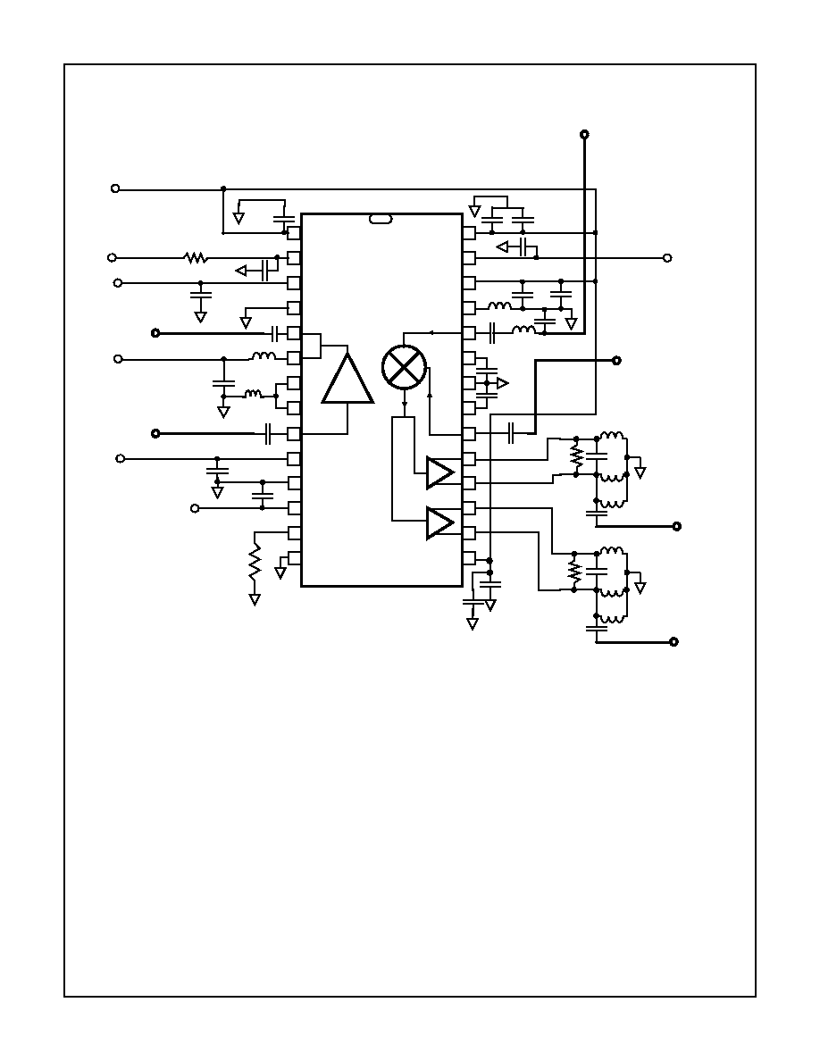
Production Test Diagram
NOTE:
4. PC trace degeneration inductor. 93mil by 8mil trace terminating in a 10mil via. Via is tied to a buried solid ground plane 12mils deep.
Material is FR4 Er = 4.7.
2
3
4
5
6
7
1
8
9
10
11
12
13
14
AGC_CTRL
PIN_O_IBIAS1
LNA_OUT
LNA_GND
LNA_IN
PIN_O_IBIAS2
PIN_I_GND
RX_PE
R_REF
BIAS_GND
BIAS_V
CC
FM_OUT+
FM_OUT-
CDMA_OUT+
CDMA_OUT-
LO_IN
RF_RET
LO_RET
MIX_GND
RF_IN
MIX_V
CC
MIX_IND
SEL
?
523 1%
0.01
HFA3665
PE
SEL
V
CC
100p
RF_LO_INPUT
MIX_V
CC
GND
8.2n
9.53k
100p
220p
220p
V
CC
15p
12p
47p
0.1
47p
220p
0.1
18n
15n
100p
4.7p
100p
0.33
2200p
2200p
AGC
LNA_OUT
C1
C3
220nH
220nH
330nH
12p
7.5p
6.6K
1.5p
R9
VLNA
220nH
220nH
330nH
12p
7.5p
6.6K
CDMA IF OUTPUT
FM IF OUTPUT
PIN BIAS 1
LNA IN
PIN BIAS 2
100p
NOTE 4
MIXER RF IN
LNA OUT
50
50
50
50
50
50
HFA3665