 | –≠–ª–µ–∫—Ç—Ä–æ–Ω–Ω—ã–π –∫–æ–º–ø–æ–Ω–µ–Ω—Ç: HFA3983 | –°–∫–∞—á–∞—Ç—å:  PDF PDF  ZIP ZIP |
4-1
TM
File Number
4635.4
CAUTION: These devices are sensitive to electrostatic discharge; follow proper IC Handling Procedures.
1-888-INTERSIL or 321-724-7143
|
Intersil and Design is a trademark of Intersil Corporation.
|
Copyright
©
Intersil Corporation 2000
PRISM is a registered trademark of Intersil Corporation. PRISM logo is a trademark of Intersil Corporation.
Further information is attainable upon NDA Agreement. NDA available on CD ROM or by contacting centapp@intersil.com.
HFA3983
2.4GHz Power Amplifier and Detector
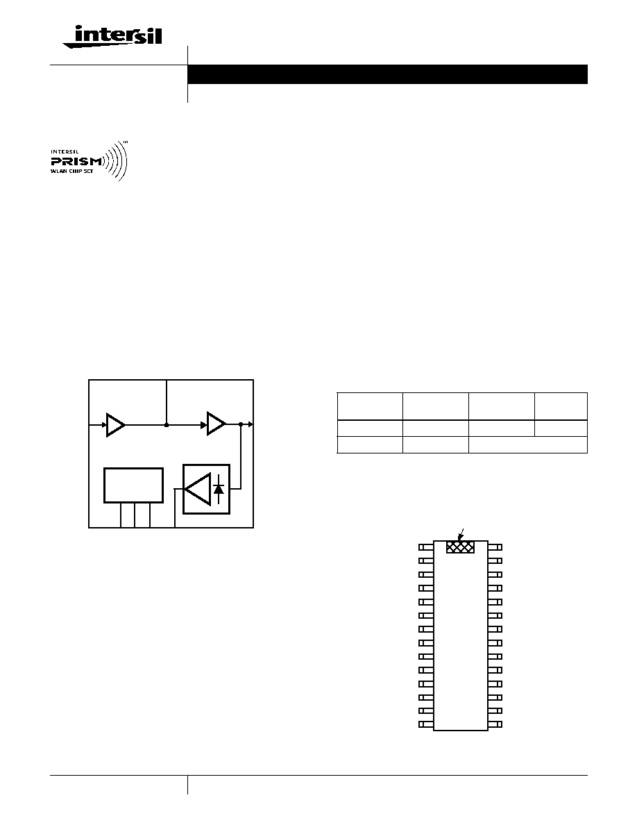
The HFA3983 is a 2.4GHz monolithic
SiGe Power Amplifier designed to
operate in the ISM Band. It features two
low voltage single supply stages.
Cascaded, they deliver a 18dBm (Typ.)
of an output power for the typical DSSS signal (ACPR,
1st Side Lobe < -30dBc, 2nd Side Lobe < -50dBc).
In addition, the device includes a 2.4GHz detector which is
accurate over a 15dB of dynamic range with (
±
)1dB.
Therefore, an accurate ALC function can be implemented.
The HFA3983 is housed in a 28 lead exposed paddle
EPTSSOP package well suited for PCMCIA board
applications.
Simplified Block Diagram
Features
∑ Single Supply . . . . . . . . . . . . . . . . . . . . . . . . . 2.7V to 3.6V
∑ Output Power . . . . . . . . . . . 18dBm (Typ) at ACPR, DSSS,
1st Side Lobe < -30dBc, 2nd Side Lobe < -50dBc
∑ Power Gain . . . . . . . . . . . . . . . . . . . . . . . . . . . .30dB (Typ.)
∑ Detector Linear Input Power Range . . . . . . . . . . . . . .15dB
∑ Detector Accuracy
. . . . . . . . . . . . . . . . . . . . . . . . . . . . ±
1.0dB
Applications
∑ EEE802.11 1 and 2Mbps Standard
∑ Systems Targeting IEEE802.11, 11Mbps Standard
∑ Wireless Local Area Networks
∑ PCMCIA Wireless Transceivers
∑ ISM Systems Including Automatic Level Control (ALC)
∑ TDMA Packet Protocol Radios
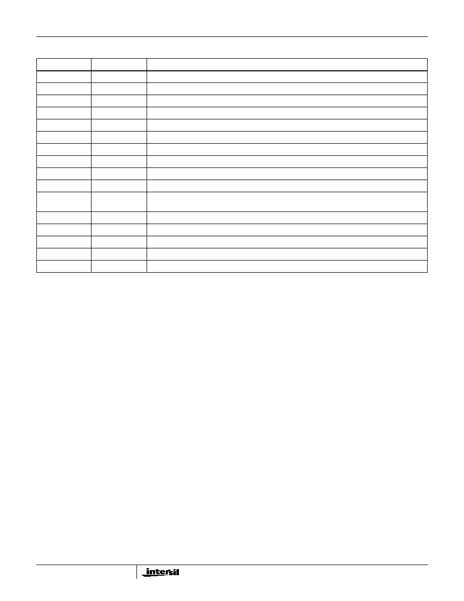
Pinout
HFA3983
(EPTSSOP)
TOP VIEW
BIAS
PEAK DETECTOR
DET_V
OUT
RF_OUT
RF_IN
DS_VCC
DS_REXT
LOG
PE
OS_REXT
Ordering Information
PART NUMBER
TEMP. RANGE
(
o
C)
PACKAGE
PKG. NO.
HFA3983IV
-40 to 85
28 Ld EPTSSOP M28.173A
HFA3983IV96
-40 to 85
Tape and Reel
INDEX AREA
GND
VCC
PE
VCC
OS_REXT
DS_REXT
GND
GND
RF_OUT
VCC
GND
DET_VOUT
GND
GND
RF_IN
GND
GND
GND
GND
DS_VCC
GND
GND
GND
GND
GND
GND
GND
GND
1
2
3
5
6
7
9
10
11
4
8
12
13
14
28
27
26
24
23
22
20
19
18
25
21
17
16
15
P
A
CKA
GE PINOUT SUBJECT T
O
CHANGE
Data Sheet
March 2000
4-2
As part of the Prism II WLAN chip set, the HFA3983 works
seamlessly with the chip set components to give you a highly
integrated, cost effective 11Mb/s WLAN solution in the 2.4 to
2.5GHz ISM band. The HFA3983 is fabricated in the fastest
SiGe BiCMOS process available, allowing superior RF
performance, normally found only in GaAs ICs. Cost
effective functions, normally requiring external components,
are integrated into one IC. The HFA3983 integrates the
following functions in one compact 28 pin EPTSSOP:
Two Stage, 30dB Gain RFPA,
Logarithmic power detect function (15dB Dynamic Range),
CMOS level compatible Power Up/Down function,
Single Supply, 2.7V to 3.6V Operation.
The HFA3983 contains a highly linear RFPA designed to
deliver 18dBm and meet an ACPR specification of -30dBc in
the 2.4 to 2.5GHz ISM band. The performance of this two
stage RFPA can be optimized by adjusting the bias current in
each stage with a dedicated resistor. No external positive or
negative power supplies are required to set the bias
currents. The on chip bias network provides the optimum
bias current temperature compensation when low TC
external resistors are used. To get the best performance
from the HFA3983, the output stage matching network can
be tailored using external components.
The HFA3983 power detect function provides a DC output
voltage that is proportional to the logarithm of the output
power. For an output power of 18dBm, the detector is
accurate to within a dB. The slope of the detector output
voltage is 100mV/dB over a 15dB dynamic range. A simple
application of the detector is to provide in-line monitoring of
the output power using a DC voltmeter. No longer is a power
meter or spectrum analyzer required. A more value added
application would use the HFA3861 Baseband Processor to
dynamically monitor the HFA3983 output power and to
control transmit power by adjusting the AGC of the HFA3783
IF Quadrature Modem to provide the best possible error free
data transfer rate for any given environment. Closed loop
power control is very important feature which compensates
for variability in the transmit chain (radio to radio, channel to
channel, over temperature...).
The HFA3983 power up/down feature integrates the power
down capability onto the IC and requires no external
components, thus freeing up board space and reducing
external component count and cost. When the CMOS
compatible PE (power enable) pin is driven low, the total
supply current drops to under 200
µ
A in, typically, 230nS.
When the PE pin is driven high, the full HFA3983 output
power is available in a few hundred nanoseconds.
In summary, the HFA3983 RFPA provides a highly cost
effective solution for the PA function by integrating many
features that would require significant development time,
drive up the total bill of materials cost and consume precious
board space. It interfaces seamlessly with the other Prism II
ICs to provide a highly integrated, cost effective 11Mb/s
WLAN solution in the 2.4 to 2.5GHz ISM band.
Pin Descriptions
PIN NUMBER
NAME
DESCRIPTION
1
GND
DC and RF Ground.
2
VCC
Power supply.
3
PE
Digital input control pin to enable the operation of the Power Amplifier. Enable logic level is High.
4
GND
DC and RF Ground.
5
VCC
Power supply.
6
OS_REXT
Output stage bias resistor, biasing scheme independent of absolute temperature.
7
DS_REXT
Driver stage bias resistor, biasing scheme independent of absolute temperature.
8
DS_VCC
Driver stage power supply.
9, 10
GND
DC and RF Ground.
11
RF_OUT
RF Output of the Power Amplifier.
12, 13, 14, 15, 16,
17, 18, 19, 20, 21
GND
DC and RF Ground.
22
RF_IN
RF Input of the Power Amplifier.
23, 24, 25
GND
DC and RF Ground.
26
DET_VOUT
Detector output.
27
GND
DC and RF Ground.
28
VCC
Power supply.
HFA3983
4-3
Absolute Maximum Ratings
Thermal Information
Supply Voltage . . . . . . . . . . . . . . . . . . . . . . . . . . . . . . . . . . . . . . . .4V
Voltage on Any Other Pin. . . . . . . . . . . . . . . . . . . -0.3 to V
CC
+0.3V
V
CC
to V
CC
Decouple . . . . . . . . . . . . . . . . . . . . . . . . . -0.3 to +0.3V
Any GND to GND. . . . . . . . . . . . . . . . . . . . . . . . . . . . . -0.3 to +0.3V
Operating Conditions
Temperature Range . . . . . . . . . . . . . . . . . . . . . . . . . . . . -40 to 85
o
C
Supply Voltage Range . . . . . . . . . . . . . . . . . . . . . . . . . . 2.7V to 3.6V
Thermal Resistance (Typical, Note 1)
JC
(
o
C/W)
EPTSSOP Package . . . . . . . . . . . . . . . . . . . . . . . . .
15
Maximum Junction Temperature (Plastic Package) . . . . . . . .150
o
C
Maximum Storage Temperature Range . . . . . . . . . . -65
o
C to 150
o
C
Maximum Lead Temperature (Soldering 10s) . . . . . . . . . . . . .300
o
C
Moisture Sensitive Level (See Tech Brief 363) . . . . . . . . 72 Hrs (L4)
CAUTION: Stresses above those listed in "Absolute Maximum Ratings" may cause permanent damage to the device. This is a stress only rating and operation of the
device at these or any other conditions above those indicated in the operational sections of this specification is not implied.
NOTE:
1.
JC
is measured with the component mounted on an evaluation PC board in free air with the exposed paddle soldered to an infinite heatsink.
General DC Electrical Specifications
PARAMETER
TEMP.
(
o
C)
MIN
TYP
MAX
UNITS
Supply Voltage
Full
2.7
-
3.6
V
Total Power Amplifier Supply Current at 3.3V, 18dBm Output
25
-
180
-
mA
RF Detector Supply Current
25
-
-
5
mA
Power Down Supply Current
Full
-
200
-
µ
A
Power Up/ Down Speed
Full
-
230
-
ns
CMOS Low Level Input Voltage
Full
-
-
0.3*V
DD
V
CMOS High Level Input Voltage (V
DD
= 3.3V)
Full
0.7*V
DD
-
3.6
V
CMOS Threshold Voltage
Full
-
0.5*V
DD
-
V
CMOS High or Low Level Input Current
Full
-10
-
+10
µ
A
Power Amplifier AC Electrical Specifications
V
CC
= 3.3V, f = 2.45GHz, Unless Otherwise Specified. Typical Application Circuit
(external input and output matching networks) has been used.
PARAMETER
TEST CONDITIONS
TEMP.
(
o
C)
MIN
TYP
MAX
UNITS
RF Frequency Range
Full
2400
-
2500
MHz
Power/Voltage Gain
Full
28
30
32
dB
Noise Figure
Full
-
-
7
dB
Input 50
VSWR
25
-
-
2.00:1
-
Output 50
VSWR
Output matching network
optimized for P1dB
compression
25
-
-
3.00:1
-
Output Power
ACPR, DSSS,
1st Side Lobe <-30dBc,
2nd Side Lobe <-50dBc
Full
17
18
dBm
Output Stability VSWR
Output Spurs Less than
-60dBc
Full
-
-
10:1
-
Output Load Mismatch
(Note 2)
Full
-
-
10:1
-
NOTE:
2. Devices sustain no damage when subjected to a mismatch of maximum 10:1.
HFA3983

4-4
HFA3983EVAL Board Schematic
TYPICAL APPLICATION EXAMPLE
Peak Detector AC Electrical Specifications
PARAMETER
TEST CONDITIONS
TEMP.
(
o
C)
MIN
TYP
MAX
UNITS
RF Output Detector Response Time
External Capacitor, C = 5pF
Full
-
0.1
1
µ
s
RF Output Detector Voltage Range
Load > 1M
Full
0
-
1.5
V
RF Output Detector Linearity
Over Linear Range
Full
-0.5
-
+0.5
dB/V
RF Output Detector Accuracy
600mVDC Output
Full
-1
-
+1
dB
RF Output Detector Slope
Over Linear Range
Full
-
10
-
dB/V
1
2
3
5
6
7
9
10
11
4
8
12
13
14
28
27
26
24
23
22
20
19
18
25
21
17
16
15
3.74k
3.74k
RFOUT (50
)
DETOUT
RFIN (50
)
V
CC
PE
BLM10A1215
V
CC
BLM31P5005
4.7
µ
F
1000pF
P1
P2
3.3V
V
CC
L
1
C
1
C
2
L
4
C
8
0.1
µ
F
V
CC
R
6
100k
C
6
1000pF
C
7
1000pF
R
4
R
5
L
2
2.2nH
L
3
BLM10A1215
C
9
0.1
µ
F
L
5
6.8nH
C
11
1000pF
C
13
1pF
C
10
2.7pF
L
6
4.7nH
C
12
7pF
C
3
270pF
R
1
1k
R
2
10
R
3
10
C
4
1000pF
C
5
1000pF
D
1
DL4001
HFA3983
4-5
Typical Performance Curves
FIGURE 1. INPUT RETURN LOSS OVER VOLTAGE
FIGURE 2. INPUT RETURN LOSS OVER TEMPERATURE
FIGURE 3. OUTPUT RETURN LOSS OVER VOLTAGE
FIGURE 4. OUTPUT RETURN LOSS OVER TEMPERATURE
FIGURE 5. LINEAR GAIN OVER VOLTAGE
FIGURE 6. LINEAR GAIN OVER TEMPERATURE
0
-12
-15
-30
2.0
2.4
2.5
3.0
INPUT RETURN LOSS (dB)
FREQUENCY (GHz)
2.7V
3.6V
0
-12
-15
-30
2.0
2.4
2.5
3.0
INPUT RETURN LOSS (dB)
FREQUENCY (GHz)
85
o
C
-40
o
C
25
o
C
0
-6
-8
-10
2.0
2.4
2.5
3.0
OUTPUT RETURN LOSS (dB)
FREQUENCY (GHz)
2.7V
3.6V
0
-5
-8
-10
2.0
2.4
2.5
3.0
INPUT RETURN LOSS (dB)
FREQUENCY (GHz)
85
o
C
-40
o
C
25
o
C
34
30
28
14
2.0
2.4
2.5
3.0
LINEAR GAIN (dB)
FREQUENCY (GHz)
2.7V
3.6V
34
30
28
14
2.0
2.4
2.5
3.0
LINEAR GAIN (dB)
FREQUENCY (GHz)
26
85
o
C
-40
o
C
25
o
C
HFA3983