 | –≠–ª–µ–∫—Ç—Ä–æ–Ω–Ω—ã–π –∫–æ–º–ø–æ–Ω–µ–Ω—Ç: HI5812JIB | –°–∫–∞—á–∞—Ç—å:  PDF PDF  ZIP ZIP |
6-1789
Semiconductor
August 1997
HI5812
CMOS 20 Microsecond, 12-Bit, Sampling A/D
Converter with Internal Track and Hold
Features
∑ Conversion Time . . . . . . . . . . . . . . . . . . . . . . . . . . . 20
µ
s
∑ Throughput Rate . . . . . . . . . . . . . . . . . . . . . . . .50 KSPS
∑ Built-In Track and Hold
∑ Guaranteed No Missing Codes Over Temperature
∑ Single Supply Voltage . . . . . . . . . . . . . . . . . . . . . . . . +5V
∑ Maximum Power Consumption. . . . . . . . . . . . . . .25mW
∑ Internal or External Clock
Applications
∑ Remote Low Power Data Acquisition Systems
∑ Digital Audio
∑ DSP Modems
∑ General Purpose DSP Front End
∑
µ
P Controlled Measurement System
∑ Professional Audio Positioner/Fader
Description
The HI5812 is a fast, low power, 12-bit, successive
approximation analog-to-digital converter. It can operate from
a single 3V to 6V supply and typically draws just 1.9mA when
operating at 5V. The HI5812 features a built-in track and hold.
The conversion time is as low as 15
µ
s with a 5V supply.
The twelve data outputs feature full high speed CMOS three-
state bus driver capability, and are latched and held through a
full conversion cycle. The output is user selectable: (i.e.) 12-
bit, 8-bit (MSBs), and/or 4-bit (LSBs). A data ready flag, and
conversion-start inputs complete the digital interface.
An internal clock is provided and is available as an output.
The clock may also be over-driven by an external source.
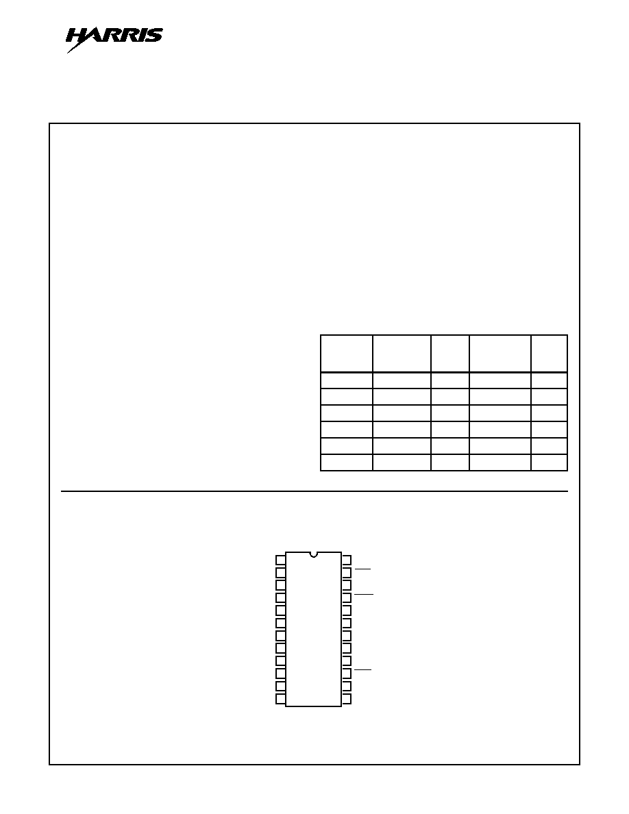
Pinout
HI5812
(PDIP, CERDIP, SOIC)
TOP VIEW
Ordering Information
PART
NUMBER
INL (LSB)
(MAX OVER
TEMP.)
TEMP.
RANGE
(
o
C)
PACKAGE
PKG.
NO.
HI5812JIP
±
1.5
-40 to 85 24 Ld PDIP
E24.3
HI5812KIP
±
1.0
-40 to 85 24 Ld PDIP
E24.3
HI5812JIB
±
1.5
-40 to 85 24 Ld SOIC
M24.3
HI5812KIB
±
1.0
-40 to 85 24 Ld SOIC
M24.3
HI5812JIJ
±
1.5
-40 to 85 24 Ld CERDIP F24.3
HI5812KIJ
±
1.0
-40 to 85 24 Ld CERDIP F24.3
1
2
3
4
5
6
7
8
9
10
11
12
DRDY
(LSB) D0
D1
D2
D3
D4
D5
D6
D7
D8
D9
V
SS
16
17
18
19
20
21
22
23
24
15
14
13
V
DD
CLK
STRT
V
REF
-
V
REF
+
V
AA
+
OEM
D11 (MSB)
D10
OEL
V
IN
V
AA
-
CAUTION: These devices are sensitive to electrostatic discharge. Users should follow proper IC Handling Procedures.
Copyright
©
Harris Corporation 1997
File Number
3214.4
6-1790
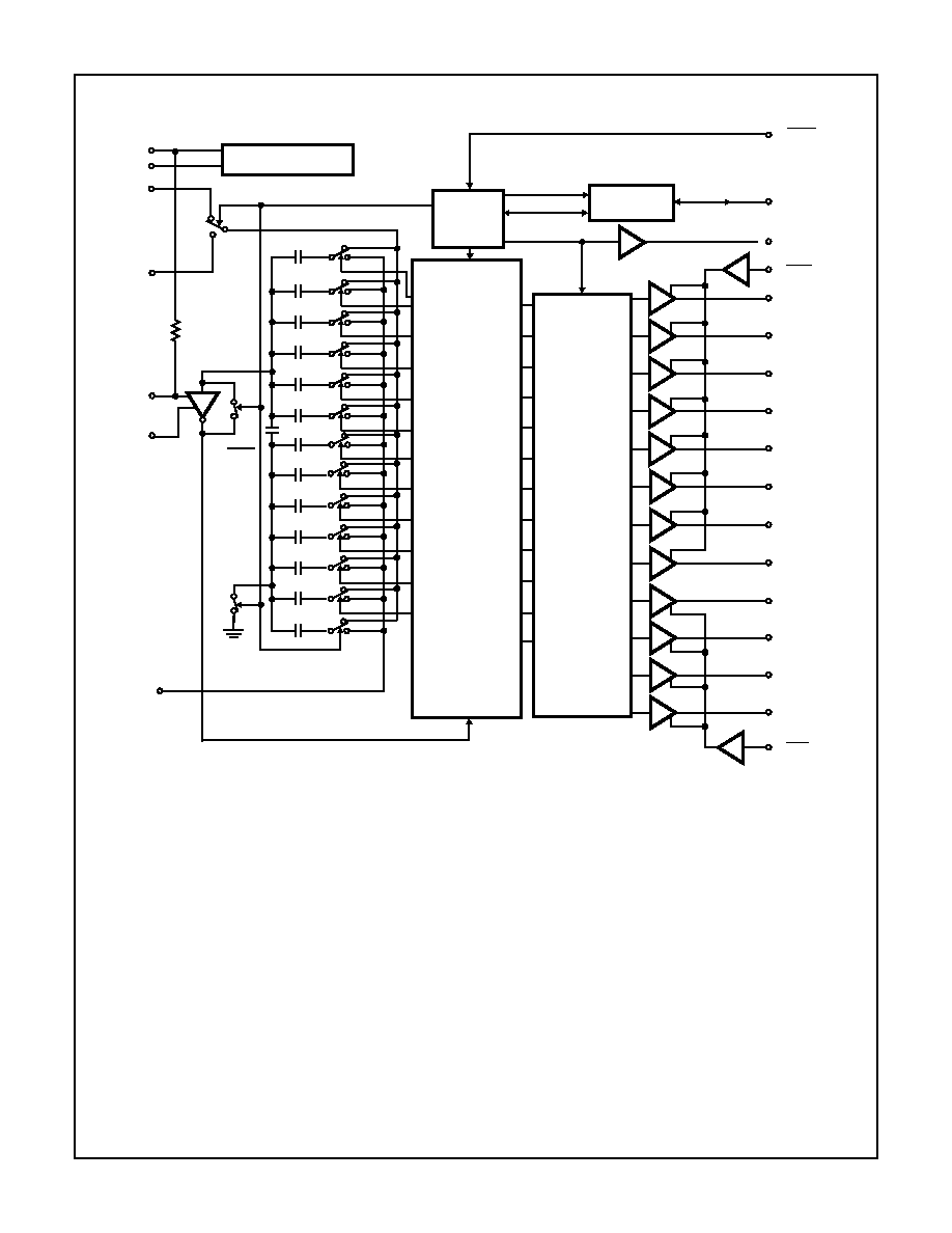
Functional Block Diagram
12-BIT
SUCCESSIVE
APPROXIMATION
REGISTER
CLOCK
TO INTERNAL LOGIC
V
DD
V
SS
V
IN
V
REF
+
V
AA
+
V
AA
-
V
REF
-
64C
63
P1
50
SUBSTRATE
16C
32C
8C
4C
2C
C
16C
32C
8C
4C
2C
C
C
CLK
DRDY
OEM
D11 (MSB)
D10
D9
D8
D7
D6
D5
D4
D3
D2
D1
D0 (LSB)
OEL
STRT
12-BIT EDGE
TRIGGERED
"D" LATCHED
CONTROL
+
TIMING
HI5812
6-1791
Absolute Maximum Ratings
Thermal Information
Supply Voltage
V
DD
to V
SS
. . . . . . . . . . . . . . . . . . . . (V
SS
-0.5V) < V
DD
< +6.5V
V
AA
+ to V
AA
-. . . . . . . . . . . . . . . . . . . . (V
SS
-0.5V) to (V
SS
+6.5V)
V
AA
+ to V
DD
. . . . . . . . . . . . . . . . . . . . . . . . . . . . . . . . . . . .
±
0.3V
Analog and Reference Inputs
V
IN
, V
REF
+, V
REF
-. . . . . . . . . (V
SS
-0.3V) < V
INA
< (V
DD
+0.3V)
Digital I/O Pins . . . . . . . . . . . . . . (V
SS
-0.3V) < VI/O < (V
DD
+0.3V)
Operating Conditions
Temperature Range
PDIP, SOIC, and CERDIP Packages . . . . . . . . . . . . . -40
o
C to 85
o
C
Thermal Resistance (Typical, Note 1)
JA
(
o
C/W)
JC
(
o
C/W)
CERDIP Package . . . . . . . . . . . . . . . .
60
12
PDIP Package . . . . . . . . . . . . . . . . . . .
80
N/A
SOIC Package . . . . . . . . . . . . . . . . . . .
75
N/A
Maximum Junction Temperature
Plastic Packages . . . . . . . . . . . . . . . . . . . . . . . . . . . . . . . . . 150
o
C
Ceramic Package . . . . . . . . . . . . . . . . . . . . . . . . . . . . . . . . 175
o
C
Maximum Storage Temperature Range . . . . . . . . . .-65
C to 150
o
C
Maximum Lead Temperature (Soldering, 10s) . . . . . . . . . . . . 300
o
C
(SOIC - Lead Tips Only)
CAUTION: Stresses above those listed in "Absolute Maximum Ratings" may cause permanent damage to the device. This is a stress only rating and operation
of the device at these or any other conditions above those indicated in the operational sections of this specification is not implied.
NOTE:
1.
JA
is measured with the component mounted on an evaluation PC board in free air.
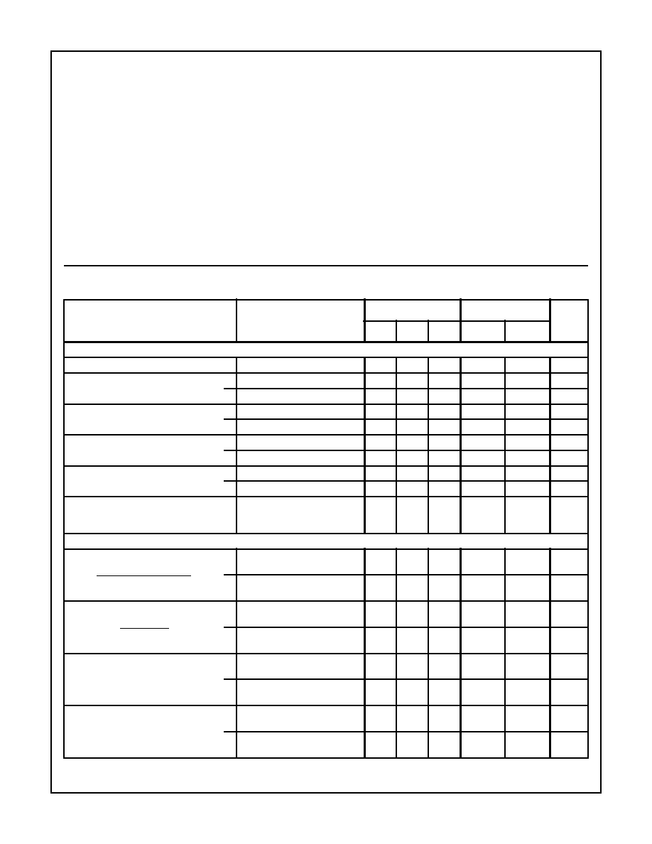
Electrical Specifications
V
DD
= V
AA
+ = 5V, V
REF
+ = +4.608V, V
SS
= V
AA
- = V
REF
- = GND, CLK = External 750kHz,
Unless Otherwise Specified
PARAMETER
TEST CONDITIONS
25
o
C
-
40
o
C TO 85
o
C
UNITS
MIN
TYP
MAX
MIN
MAX
ACCURACY
Resolution
12
-
-
12
-
Bits
Integral Linearity Error, INL
(End Point)
J
-
-
±
1.5
-
±
1.5
LSB
K
-
-
±
1.0
-
±
1.0
LSB
Differential Linearity Error, DNL
J
-
-
±
2.0
-
±
2.0
LSB
K
-
-
±
1.0
-
±
1.0
LSB
Gain Error, FSE
(Adjustable to Zero)
J
-
-
±
3.0
-
±
3.0
LSB
K
-
-
±
2.5
-
±
2.5
LSB
Offset Error, V
OS
(Adjustable to Zero)
J
-
-
±
2.0
-
±
2.0
LSB
K
-
-
±
1.0
-
±
1.0
LSB
Power Supply Rejection, PSRR
Offset Error PSRR
Gain Error PSRR
V
REF
= 4V
V
DD
=
V
AA
+ = 5V
±
5%
V
DD
=
V
AA
+ = 5V
±
5%
0.1
0.1
±
0.5
±
0.5
±
0.5
±
0.5
LSB
LSB
DYNAMIC CHARACTERISTICS
Signal to Noise Ratio, SINAD
RMS Signal
RMS Noise + Distortion
J
f
S
= Internal Clock, f
IN
= 1kHz
f
S
= 750kHz, f
IN
= 1kHz
-
68.8
69.2
-
-
-
dB
dB
K
f
S
= Internal Clock, f
IN
= 1kHz
f
S
= 750kHz, f
IN
= 1kHz
-
71.0
71.5
-
-
-
dB
dB
Signal to Noise Ratio, SNR
RMS Signal
RMS Noise
J
f
S
= Internal Clock, f
IN
= 1kHz
f
S
= 750kHz, f
IN
= 1kHz
-
70.5
71.1
-
-
-
dB
dB
K
f
S
= Internal Clock, f
IN
= 1kHz
f
S
= 750kHz, f
IN
= 1kHz
-
71.5
72.1
-
-
-
dB
dB
Total Harmonic Distortion, THD
J
f
S
= Internal Clock, f
IN
= 1kHz
f
S
= 750kHz, f
IN
= 1kHz
-
-73.9
-73.8
-
-
-
dBc
dBc
K
f
S
= Internal Clock, f
IN
= 1kHz
f
S
= 750kHz, f
IN
= 1kHz
-80.3
-79.0
-
-
-
dBc
dBc
Spurious Free Dynamic Range,
SFDR
J
f
S
=Internal Clock, f
IN
= 1kHz
f
S
= 750kHz, f
IN
= 1kHz
-
-75.4
-75.1
-
-
-
dB
dB
K
f
S
= Internal Clock, f
IN
= 1kHz
f
S
= 750kHz, f
IN
= 1kHz
-
-80.9
-79.6
-
-
-
dB
dB
HI5812
6-1792
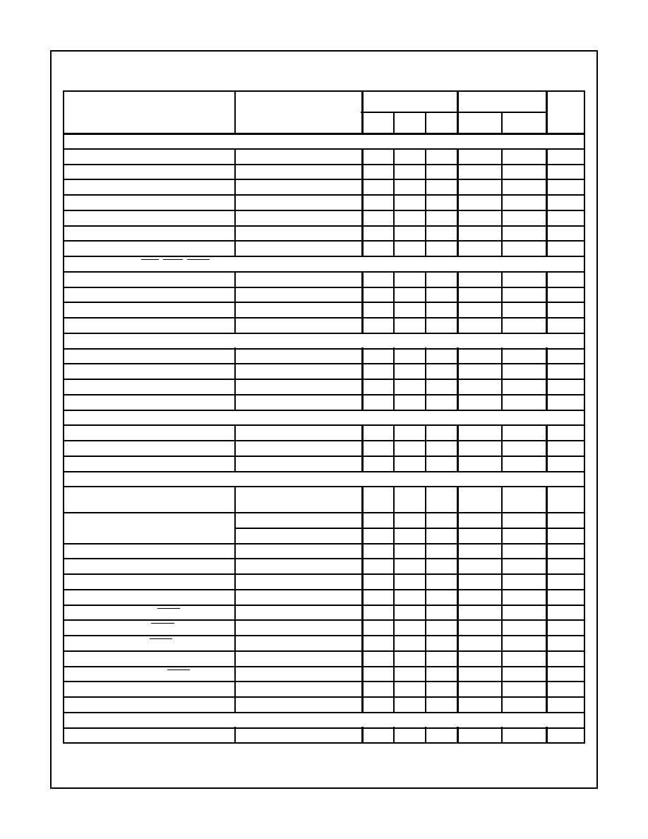
ANALOG INPUT
Input Current, Dynamic
At V
IN
= V
REF
+, 0V
-
±
50
±
100
-
±
100
µ
A
Input Current, Static
Conversion Stopped
-
±
0.4
±
10
-
±
10
µ
A
Input Bandwidth -3dB
-
1
-
-
-
MHz
Reference Input Current
-
160
-
-
-
µ
A
Input Series Resistance, R
S
In Series with Input C
SAMPLE
-
420
-
-
-
Input Capacitance, C
SAMPLE
During Sample State
-
380
-
-
-
pF
Input Capacitance, C
HOLD
During Hold State
-
20
-
-
-
pF
DIGITAL INPUTS OEL, OEM, STRT
High-Level Input Voltage, V
IH
2.4
-
-
2.4
-
V
Low-Level Input Voltage, V
IL
-
-
0.8
-
0.8
V
Input Leakage Current, I
IL
Except CLK, V
IN
= 0V, 5V
-
-
±
10
-
±
10
µ
A
Input Capacitance, C
IN
-
10
-
-
-
pF
DIGITAL OUTPUTS
High-Level Output Voltage, V
OH
I
SOURCE
= -400
µ
A
4.6
-
-
4.6
-
V
Low-Level Output Voltage, V
OL
I
SINK
= 1.6mA
-
-
0.4
-
0.4
V
Three-State Leakage, I
OZ
Except DRDY, V
OUT
= 0V, 5V
-
-
±
10
-
±
10
µ
A
Output Capacitance, C
OUT
Except DRDY
-
20
-
-
-
pF
CLOCK
High-Level Output Voltage, V
OH
I
SOURCE
= -100
µ
A (Note 2)
4
-
-
4
-
V
Low-Level Output Voltage, V
OL
I
SINK
= 100
µ
A (Note 2)
-
-
1
-
1
V
Input Current
CLK Only, V
IN
= 0V, 5V
-
-
±
5
-
±
5
mA
TIMING
Conversion Time (t
CONV
+ t
ACQ
)
(Includes Acquisition Time)
20
-
-
20
-
µ
s
Clock Frequency
Internal Clock, (CLK = Open)
200
300
400
150
500
kHz
External CLK (Note 2)
0.05
2
1.5
0.05
1.5
MHz
Clock Pulse Width, t
LOW
, t
HIGH
External CLK (Note 2)
100
-
-
100
-
ns
Aperture Delay, t
D
APR
(Note 2)
-
35
50
-
70
ns
Clock to Data Ready Delay, t
D1
DRDY
(Note 2)
-
105
150
-
180
ns
Clock to Data Ready Delay, t
D2
DRDY
(Note 2)
-
100
160
-
195
ns
Start Removal Time, t
R
STRT
(Note 2)
75
30
-
75
-
ns
Start Setup Time, t
SU
STRT
(Note 2)
85
60
-
100
-
ns
Start Pulse Width, t
W
STRT
(Note 2)
10
4
-
15
-
ns
Start to Data Ready Delay, t
D3
DRDY
(Note 2)
-
65
105
-
120
ns
Clock Delay from Start, t
D
STRT
(Note 2)
-
60
-
-
-
ns
Output Enable Delay, t
EN
(Note 2)
-
20
30
-
50
ns
Output Disabled Delay, t
DIS
(Note 2)
-
80
95
-
120
ns
POWER SUPPLY CHARACTERISTICS
Supply Current, I
DD
+ I
AA
-
1.9
5
-
8
mA
NOTE:
2. Parameter guaranteed by design or characterization, not production tested.
Electrical Specifications
V
DD
= V
AA
+ = 5V, V
REF
+ = +4.608V, V
SS
= V
AA
- = V
REF
- = GND, CLK = External 750kHz,
Unless Otherwise Specified (Continued)
PARAMETER
TEST CONDITIONS
25
o
C
-
40
o
C TO 85
o
C
UNITS
MIN
TYP
MAX
MIN
MAX
HI5812
6-1793
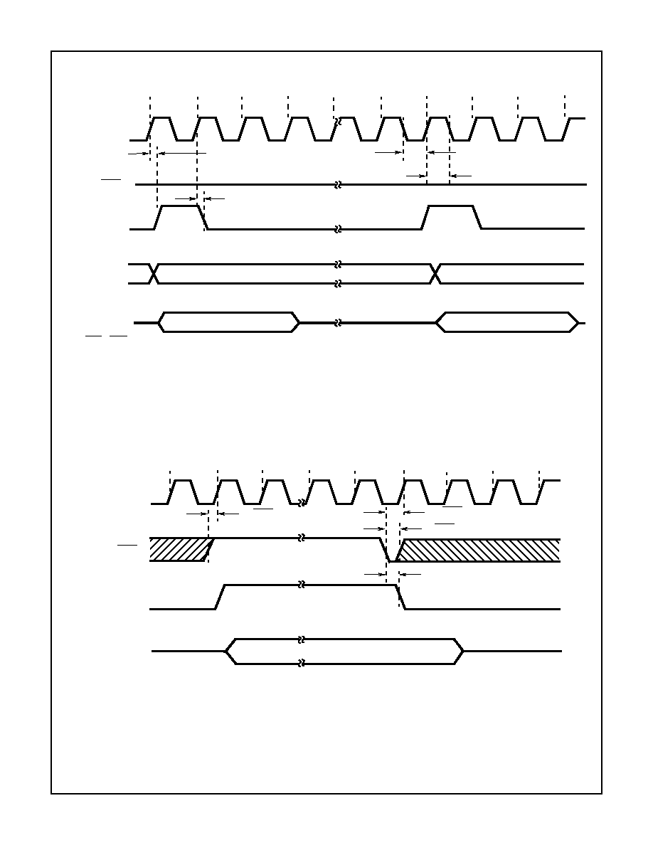
Timing Diagrams
FIGURE 1. CONTINUOUS CONVERSION MODE
FIGURE 2. SINGLE SHOT MODE EXTERNAL CLOCK
D0 - D11
CLK
(EXTERNAL
t
D2
DRDY
t
LOW
t
HIGH
1
2
3
4
5 - 14
15
1
2
3
STRT
OR INTERNAL)
HOLD N
TRACK N
TRACK N + 1
V
IN
OEL = OEM = V
SS
DRDY
t
D1
DRDY
DATA N - 1
DATA N
STRT
HOLD
TRACK
HOLD
CLK
(EXTERNAL)
DRDY
V
IN
t
R
STRT
t
SU
STRT
t
W
STRT
15
1
2
2
2
3
4
5
t
D3
DRDY
HI5812