
1871
Semiconductor
March 1998
HI7190
24-Bit, High Precision,
Sigma Delta A/D Converter
Features
∑ 22-Bit Resolution with No Missing Code
∑ 0.0007% Integral Non-Linearity (Typ)
∑ 20mV to
±
2.5V Full Scale Input Ranges
∑ Internal PGIA with Gains of 1 to 128
∑ Serial Data I/O Interface, SPI Compatible
∑ Differential Analog and Reference Inputs
∑ Internal or System Calibration
∑ -120dB Rejection of 60/50Hz Line Noise
∑ Settling Time of 4 Conversions (Max) for a Step Input
Applications
∑ Process Control and Measurement
∑ Industrial Weight Scales
∑ Part Counting Scales
∑ Laboratory Instrumentation
∑ Seismic Monitoring
∑ Magnetic Field Monitoring
∑ Additional Reference Literature
- TB348 "HI7190/1 Negative Full Scale Error vs
Conversion Frequency"
- AN9504 "A Brief Intro to Sigma Delta Conversion"
- TB329 "Harris Sigma Delta Calibration Technique"
- AN9505 "Using the HI7190 Evaluation Kit"
- TB331 "Using the HI7190 Serial Interface"
- AN9527 "Interfacing HI7190 to a Microcontroller"
- AN9532 "Using HI7190 in a Multiplexed System"
- AN9601 "Using HI7190 with a Single +5V Supply"
Description
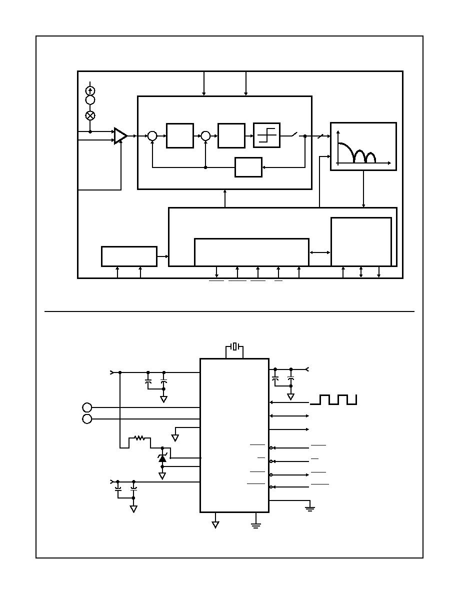
The Harris HI7190 is a monolithic instrumentation, sigma delta
A/D converter which operates from
±
5V supplies. Both the sig-
nal and reference inputs are fully differential for maximum flexi-
bility and performance. An internal Programmable Gain
Instrumentation Amplifier (PGIA) provides input gains from 1 to
128 eliminating the need for external pre-amplifiers. The on-
demand converter auto-calibrate function is capable of remov-
ing offset and gain errors existing in external and internal cir-
cuitry. The on-board user programmable digital filter provides
over -120dB of 60/50Hz noise rejection and allows fine tuning
of resolution and conversion speed over a wide dynamic range.
The HI7190 and HI7191 are functionally the same device so all
discussion will refer to the HI7190 for simplicity.
The HI7190 contains a serial I/O port and is compatible with
most synchronous transfer formats including both the Motor-
ola 6805/11 series SPI and Intel 8051 series SSR protocols.
A sophisticated set of commands gives the user control over
calibration, PGIA gain, device selection, standby mode, and
several other features. The On-chip Calibration Registers
allow the user to read and write calibration data.
Pinout
HI7190
(PDIP, SOIC)
TOP VIEW
Ordering Information
PART NUMBER
TEMP.
RANGE (
o
C)
PACKAGE
PKG.
NO.
HI7190IP
-40 to 85
20 Ld PDIP
E20.3
HI7190IB
-40 to 85
20 Ld SOIC
M20.3
HI7190EVAL
Evaluation Kit
11
12
13
14
15
16
17
18
20
19
10
9
8
7
6
5
4
3
2
1
SCLK
SDO
SDIO
CS
DRDY
DGND
V
RLO
AV
SS
V
RHI
V
CM
MODE
RESET
OSC
1
OSC
2
SYNC
DV
DD
AGND
AV
DD
V
INHI
V
INLO
CAUTION: These devices are sensitive to electrostatic discharge. Users should follow proper IC Handling Procedures.
Copyright
©
Harris Corporation 1998
File Number
3612.5
1872
Functional Block Diagram
Typical Application Schematic
DIGITAL FILTER
-
MODULATOR
PGIA
1-BIT
D/A
1
CONTROL AND SERIAL INTERFACE UNIT
CONTROL REGISTER
SERIAL INTERFACE
UNIT
CLOCK
GENERATOR
AV
DD
TRANSDUCER
BURN-OUT
CURRENT
V
INHI
V
INLO
V
CM
OSC
1
OSC
2
DRDY RESET SYNC
CS
MODE
S
CLK
SDIO
SDO
V
RHI
V
RLO
REFERENCE
INPUTS
10MHz
OSC
1
OSC
2
V
RHI
V
RLO
+2.5V
AV
DD
+5V
0.1uF
V
CM
V
INHI
V
INLO
AGND
DV
DD
DGND
SCLK
CS
DRDY
SYNC
SDO
SDIO
+5V
4.7
µ
F
+
0.1
µ
F
4.7
µ
F
+
RESET
INPUT
INPUT
AV
SS
-5V
0.1
µ
F
4.7
µ
F
+
DATA I/O
DATA OUT
SYNC
CS
DRDY
RESET
13
17
16
15
12
11
10
9
8
7
14
6
18
5
4
19
2
3
1
MODE
20
REFERENCE
+
-
R
1
HI7190

1873
Absolute Maximum Ratings
Thermal Information
Supply Voltage
AV
DD
to AGND . . . . . . . . . . . . . . . . . . . . . . . . . . . . . . . . . . . +5.5V
AV
SS
to AGND . . . . . . . . . . . . . . . . . . . . . . . . . . . . . . . . . . . -5.5V
DV
DD
to DGND . . . . . . . . . . . . . . . . . . . . . . . . . . . . . . . . . . +5.5V
DGND to AGND . . . . . . . . . . . . . . . . . . . . . . . . . . . . . . . . .
±
0.3V
Analog Input Pins . . . . . . . . . . . . . . . . . . . . . . . . . . . . AV
SS
to AV
DD
Digital Input, Output and I/O Pins . . . . . . . . . . . . . . . DGND to DV
DD
ESD Tolerance (No Damage)
Human Body Model . . . . . . . . . . . . . . . . . . . . . . . . . . . . . . . 500V
Machine Model . . . . . . . . . . . . . . . . . . . . . . . . . . . . . . . . . . +100V
Charged Device Model . . . . . . . . . . . . . . . . . . . . . . . . . . . . 1000V
Operating Conditions
Temperature Range . . . . . . . . . . . . . . . . . . . . . . . . . . -40
o
C to 85
o
C
Thermal Resistance (Typical, Note 1)
JA
(
o
C/W)
PDIP Package . . . . . . . . . . . . . . . . . . . . . . . . . . . . .
125
SOIC Package . . . . . . . . . . . . . . . . . . . . . . . . . . . . .
100
Maximum Junction Temperature
Plastic Packages . . . . . . . . . . . . . . . . . . . . . . . . . . . . . . . . . 150
o
C
Maximum Storage Temperature Range . . . . . . . . . .-65
o
C to 150
o
C
Maximum Lead Temperature (Soldering, 10s) . . . . . . . . . . . . 300
o
C
(SOIC - Lead Tips Only)
CAUTION: Stresses above those listed in "Absolute Maximum Ratings" may cause permanent damage to the device. This is a stress only rating and operation
of the device at these or any other conditions above those indicated in the operational sections of this specification is not implied.
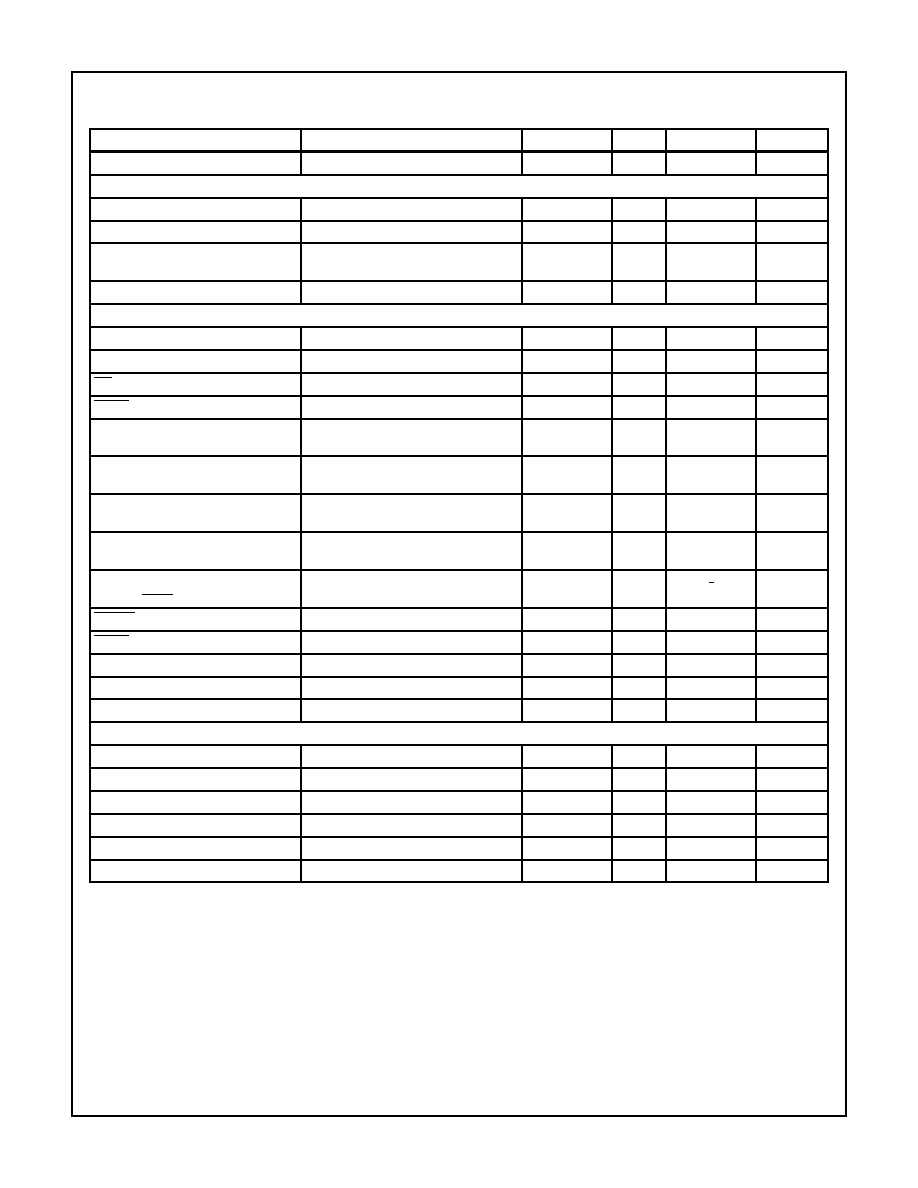
Electrical Specifications
AV
DD
= +5V, AV
SS
= -5V, DV
DD
= +5V, V
RHI
= +2.5V, V
RLO
= AGND = 0V, V
CM
= AGND,
PGIA Gain = 1, OSC
IN
= 10MHz, Bipolar Input Range Selected, f
N
= 10Hz
PARAMETER
TEST CONDITIONS
MIN
TYP
MAX
UNITS
SYSTEM PERFORMANCE
Integral Non-Linearity, INL
End Point Line Method (Notes 3, 5, 6)
-
±
0.0007
±
0.0015
%FS
Differential Non-Linearity
(Note 2)
No Missing codes to 22-Bits
LSB
Offset Error, V
OS
See Table 1
-
-
-
-
Offset Error Drift
V
INHI
= V
INLO
(Notes 3, 8)
-
1
-
µ
V/
o
C
Full Scale Error, FSE
V
INHI
- V
INLO
= +2.5V (Notes 3, 5, 8, 10)
-
-
-
-
Noise, e
N
See Table 1
-
-
-
-
Common Mode Rejection Ratio, CMRR V
CM
= 0V, V
INHI
= V
INLO
from -2V to +2V
-70
-
dB
Normal Mode 50Hz Rejection
Filter Notch = 10Hz, 25Hz, 50Hz (Note 2)
-120
-
-
dB
Normal Mode 60Hz Rejection
Filter Notch = 10Hz, 30Hz, 60Hz (Note 2)
-120
-
-
dB
Step Response Settling Time
-
2
4
Conversions
ANALOG INPUTS
Input Voltage Range
Unipolar Mode (Note 9)
0
-
V
REF
V
Input Voltage Range
Bipolar Mode (Note 9)
- V
REF
-
V
REF
V
Common Mode Input Range
(Note 2)
AV
SS
-
AV
DD
V
Input Leakage Current, I
IN
V
IN
= AV
DD
(Note 2)
-
-
1.0
nA
Input Capacitance, C
IN
-
5.0
-
pF
Reference Voltage Range, V
REF
(V
REF
= V
RHI
- V
RLO
)
2.5
-
5
V
Transducer Burn-Out Current, I
BO
-
200
-
nA
CALIBRATION LIMITS
Positive Full Scale Calibration Limit
-
-
1.2(V
REF
/Gain)
-
Negative Full Scale Calibration Limit
-
-
1.2(V
REF
/Gain)
-
Offset Calibration Limit
-
-
1.2(V
REF
/Gain)
-
Input Span
0.2(V
REF
/Gain)
-
2.4(V
REF
/Gain)
-
DIGITAL INPUTS
Input Logic High Voltage, V
IH
(Note 11)
2.0
-
-
V
Input Logic Low Voltage, V
IL
-
-
0.8
V
Input Logic Current, I
I
V
IN
= 0V, +5V
-
1.0
10
µ
A
HI7190
1874
Input Capacitance, C
IN
V
IN
= 0V
-
5.0
-
pF
DIGITAL OUTPUTS
Output Logic High Voltage, V
OH
I
OUT
= -100
µ
A (Note 7)
2.4
-
-
V
Output Logic Low Voltage, V
OL
I
OUT
= 3mA (Note 7)
-
-
0.4
V
Output Three-State Leakage Current,
I
OZ
V
OUT
= 0V, +5V (Note 7)
-10
1
10
µ
A
Digital Output Capacitance, C
OUT
-
10
-
pF
TIMING CHARACTERISTICS
SCLK Minimum Cycle Time, t
SCLK
200
-
-
ns
SCLK Minimum Pulse Width, t
SCLKPW
50
-
-
ns
CS to SCLK Precharge Time, t
PRE
50
-
-
ns
DRDY Minimum High Pulse Width
(Notes 2, 7)
500
-
-
ns
Data Setup to SCLK Rising Edge
(Write), t
DSU
50
-
-
ns
Data Hold from SCLK Rising Edge
(Write), t
DHLD
0
-
-
ns
Data Read Access from Instruction
Byte Write, t
ACC
(Note 7)
-
-
40
ns
Read Bit Valid from SCLK Falling Edge,
t
DV
(Note 7)
-
-
40
ns
Last Data Transfer to Data Ready
Inactive, t
DRDY
(Note 7)
-
35
-
ns
RESET Low Pulse Width
(Note 2)
100
-
-
ns
SYNC Low Pulse Width
(Note 2)
100
-
-
ns
Oscillator Clock Frequency
(Note 2)
0.1
-
10
MHz
Output Rise/Fall Time
(Note 2)
-
-
30
ns
Input Rise/Fall Time
(Note 2)
-
-
1
µ
s
POWER SUPPLY CHARACTERISTICS
IAV
DD
-
-
1.5
mA
IAV
SS
-
-
1.5
mA
IDV
DD
SCLK = 4MHz
-
-
3.0
mA
Power Dissipation, Active PD
A
SB = `0'
-
15
30
mW
Power Dissipation, Standby PD
S
SB = `1'
-
5
-
mW
PSRR
(Note 3)
-
-70
-
dB
NOTES:
1.
JA
is measured with the component mounted on an evaluation PC board in free air.
2. Parameter guaranteed by design or characterization, not production tested.
3. Applies to both bipolar and unipolar input ranges.
4. These errors can be removed by re-calibrating at the desired operating temperature.
5. Applies after system calibration.
6. Fully differential input signal source is used.
7. See Load Test Circuit, Figure 10, R1 = 10k
, C
L
= 50pF.
8. 1 LSB = 298nV at 24 bits for a Full Scale Range of 5V.
9. V
REF
= V
RHI
- V
RLO
10. These errors are on the order of the output noise shown in Table 1.
11. All inputs except OSC
1
. The OSC
1
input V
IH
is 3.5V minimum.
Electrical Specifications
AV
DD
= +5V, AV
SS
= -5V, DV
DD
= +5V, V
RHI
= +2.5V, V
RLO
= AGND = 0V, V
CM
= AGND,
PGIA Gain = 1, OSC
IN
= 10MHz, Bipolar Input Range Selected, f
N
= 10Hz (Continued)
PARAMETER
TEST CONDITIONS
MIN
TYP
MAX
UNITS
HI7190
1875
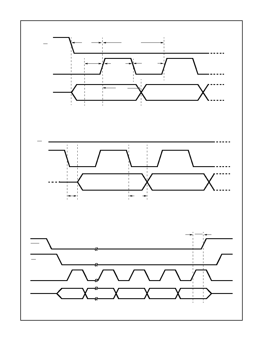
Timing Diagrams
FIGURE 1. DATA WRITE TO HI7190
FIGURE 2. DATA READ FROM HI7190
FIGURE 3. DATA READ FROM HI7190
1ST BIT
2ND BIT
CS
SCLK
SDIO
t
SCLK
t
DSU
t
DHLD
t
SCLKPW
t
SCLKPW
t
PRE
CS
SCLK
SDIO
SDO
t
ACC
t
DV
1ST BIT
2ND BIT
SCLK
CS
DRDY
SDIO
t
DRDY
8
7
6
5
1
HI7190