 | –≠–ª–µ–∫—Ç—Ä–æ–Ω–Ω—ã–π –∫–æ–º–ø–æ–Ω–µ–Ω—Ç: HIP0045AB | –°–∫–∞—á–∞—Ç—å:  PDF PDF  ZIP ZIP |
4-1
File Number
4047.2
HIP0045
1A/50V Octal Low Side Power Driver With
Serial Bus Control and Fault Protection
The HIP0045 is a logic controlled, eight channel Octal Serial
Power Low Side Driver. The serial peripheral interface (SPI)
utilized by the HIP0045 is a serial synchronous bus compatible
with Intersil CDP68HC05, or equivalent, microcomputers. As
shown in the Block Diagram for the HIP0045, each of the open
drain MOS Output Drivers have individual protection for over-
voltage and over-current. Each output channel has separate
output latch control with fault unlatch and diagnostic or status
feedback. Under normal ON conditions, each output driver is in
a low voltage, high current state of saturated turn-on.
Comparators in the diagnostic circuitry monitor the output
drivers to determine if an out of saturation condition exists. If a
fault is sensed, the respective output driver for Channels 0 - 5
have overcurrent latch-off. Channels 6 and 7 are configured for
lamp drivers and have current limiting with over-temperature
latch-off. Channels 0 and 1 have direct parallel drive control for
PWM applications and are ORed with the SPI Bus control. All
channels are SPI Bus controlled and sense the output states
for diagnostic feedback.
The HIP0045 is fabricated in a Power BiMOS IC process,
and is intended for use in automotive and other applications
having a wide range of temperature and electrical stress
conditions. It is particularly suited for driving relays,
solenoids and lamps in applications where low standby
power, high operating voltage, and high output current in
high ambient temperature conditions is required.
The HIP0045 is in a 20 lead plastic Power SOP (PSOP)
Package with an integral copper `slug' to conduct heat directly
to a PCB interface or heat sink on the bottom of the package.
Driver Block Diagram
Features
∑ Octal NDMOS Output Drivers in a High Voltage Power
BiMOS Process
∑ Over-Stress Protection - Each Output:
- Over-Current Protection . . . . . . . . . . . . . . . . . . . 1A Min
- Over-Voltage Clamp Protection . . . . . . . . . . . . 50V Typ
- Thermal Shutdown Protection (2 Channels)
∑ Open-Load Detection
∑ Power BiMOS Output Configuration
- Current Latch-Off Protection for 6 Channels; 2 with
External Drive Input and ORed with SPI Bus Control
- 2 Channels Configured for Lamp Drivers with Current
Limiting and Over-Temperature Latch-Off
∑ High Speed CMOS Logic Control
- SPI Bus Controlled Interface
- Individual Output Latch
- Individual Fault Unlatch and Feedback
- Common Reset Line
∑ Low Quiescent Current . . . . . . . . . . . . . . . . . . . 5mA Max
∑ Ambient Operating Temp. Range . . . . . . . -40
o
C to 125
o
C
Applications
∑ Automotive and Industrial Systems
∑ Solenoids, Relays and Lamp Drivers
∑ Logic and
µ
P Controlled Drivers
∑ Robotic Controls
Pinout
HIP0045 (PSOP WITH HEAT SLUG)
TOP VIEW
Ordering Information
PART NO.
TEMP. RANGE (
o
C)
PACKAGE
PKG. NO.
HIP0045AB
-40 to 125
20 Ld PSOP
M20.433
OUT
DRIVER
V
CC
OC
FAULT/STATUS
REF
V
REF
OVER-TEMP.
DET. (CH. 6, 7)
SPI AND
DIRECT
INPUT
CONTROL
WITH
FAULT/
STATUS
RESET
OUTPUT
OC LATCH
(CH. 0-5)
I
SK
OC LIMIT
(CH. 6, 7)
-
+
-
+
INTEGRAL COPPER
HEAT SINK `SLUG'
FOR PCB CONTACT
OR EXT. HEAT SINK
1
2
3
4
5
6
7
8
9
10
20
19
18
17
16
15
14
13
12
11
GND
IN0
MISO
OUT0
OUT2
OUT4
OUT6
MOSI
SCK
GND
GND
CE
RESET
OUT7
OUT5
OUT3
OUT1
V
CC
IN1
GND
Data Sheet
April 1999
CAUTION: These devices are sensitive to electrostatic discharge; follow proper IC Handling Procedures.
http://www.intersil.com or 407-727-9207
|
Copyright
©
Intersil Corporation 1999
4-2
Detailed Block Diagram
Input to Output Control Tables
OUT2-5
DRIVER
V
CC
OC
REF
V
REF
I
SK
-
+
-
+
Q
S
R
Q2 - 5
ON/OFF
LATCH
DIAG2-5
STATUS
OUT6, 7
DRIVER
V
CC
OC
REF
V
REF
I
SK
-
+
-
+
Q
S
R
Q6, 7
ON/OFF
LATCH
DIAG6, 7
STATUS
OVER-TEMP.
DET.
OUT0, 1
DRIVER
V
CC
OC
REF
V
REF
I
SK
-
+
Q
S
R
OVERLOAD LATCH
V
CC
IN 0, 1
Q0, 1
ON/OFF
SCK
MOSI
8-BIT
OUTPUT
LATCH
Q0-7
DIAG 0-7
MISO
D
Q
RESET
LOW
VOTAGE
RESET
RESET
CE
V
CC
SPI
SHIFT
REG
OUT
IN
V
CC
V
CC
V
CC
NOTES:
1. OC = Over-Current Voltage Ref. = 1.8V Typ.
2. I
SK
= Current Sink Pull-Down = 500
µ
A Typ.
3. Diag0, 1 = Status bit when Q0, 1 controlling OUT0, 1.
4. Diag0, 1 = Fault bit when IN1, 0 controlling OUT0, 1.
5. Refer to text and Tables 6, 7 for diagnostic information.
STATUS/
FAULT LATCH
FILTER
FAULT
RESET
FILTER
RESET
Q
S
R
DIAG 0, 1
OVERLOAD LATCH
OVERLOAD LATCH
LATCH
-
+
TABLE 1. OUTPUT 0
SPI BIT 0
IN0
OUT0
0
1
OFF
0
0
ON
1
0
ON
1
1
ON
TABLE 2. OUTPUT 1
SPI BIT 1
IN1
OUT1
0
1
OFF
0
0
ON
1
0
ON
1
1
ON
TABLE 3. OUTPUT 2 - 7
SPI BIT 2 - 7
OUT2 - 7
0
OFF
1
ON
TABLE 4. OUTPUT CONTROL REGISTER, Q0 - 7
Q1
Q3
Q5
Q7
Q0
Q2
Q4
Q6
(D7I)
(D6I)
(D5I)
(D4I)
(D3I)
(D2I)
(D1I)
(D0I)
MSB
LSB
NOTE:
The Output Control Register bits Q0 -7 have the same order
as the Diagnostic Failure Register bits Diag0 - 7 as defined in Table 5.
Data bits D0I - D7I give the MOSI SPI serial data input flow
sequence.
HIP0045
4-3
Absolute Maximum Ratings
Thermal Information
Maximum Output Voltage, V
OUT
. . . . . . . . . . . . . . . . . . .-0.7 to V
OC
Peak Output Load Current, I
LOAD
. . . . . As Specified for I
SC
, I
LIM
Continuous Output Load Current, I
OUT
(All 8 Outputs ON) . . . . 0.5A
Continuous Output Load Current, I
OUT
(Any one Output ON) . . 1A
Total Average Current, I
OUT
(All 8 Outputs) . . . . . . . . . . . . . . . 4.5A
Reverse Peak Current Drive, Any one Output, I
RD
; t
2ms . . . -3A
DC Logic Supply, V
CC
. . . . . . . . . . . . . . . . . . . . . . . . . . . . -0.3 to 7V
Input Voltage, All Inputs and Data Lines . . . . . . . -0.3 to V
CC
+0.3V
Operating Conditions
Temperature Range . . . . . . . . . . . . . . . . . . . . . . . . . -40
o
C to 125
o
C
Logic Supply Voltage, V
CC
. . . . . . . . . . . . . . . . . . . . . 4.5V to 5.5V
Thermal Resistance (Typical, Note 6)
JA
(
o
C/W)
JC
(
o
C/W)
PSOP Package . . . . . . . . . . . . . . . . . .
40
2
Maximum Junction Temperature, T
J
. . . . . . . . . . . . . . . . . . . .150
o
C
Maximum Storage Temperature Range, T
STG
. . . . -55
o
C to 150
o
C
Maximum Lead Temperature (Soldering 10s) . . . . . . . . . . . . .265
o
C
Die Characteristics
Back Side Potential . . . . . . . . . . . . . . . . . . .V- (GND Pin, Heat Sink)
CAUTION: Stresses above those listed in "Absolute Maximum Ratings" may cause permanent damage to the device. This is a stress only rating and operation of the
device at these or any other conditions above those indicated in the operational sections of this specification is not implied.
NOTE:
6.
JA
Rated with standard PC Board,
JC
rated with infinite heat sink.
Electrical Specifications
V
CC
= 4.5V to 5.5V, T
A
= -40
o
C to 125
o
C, Unless Otherwise Specified
PARAMETER
SYMBOL
TEST CONDITIONS
MIN
TYP
MAX
UNITS
Standby Current, No Load
I
CCO
No Load
-
-
5
mA
Supply Current, Full Load
I
CC
All Outputs ON, 0.5A Load Per Output
-
-
5
mA
Output Clamping Voltage (Note 7)
V
OC
I
LOAD
= 0.5A, Output Programmed OFF
45
-
62
V
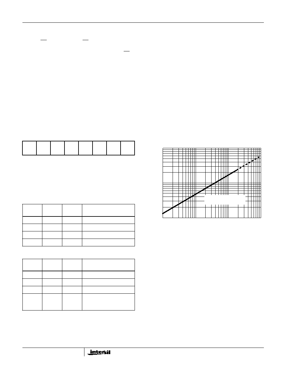
Output Clamping Energy
E
OC
1ms Single Pulse Width, T
A
= 25
o
C,
(Refer to Figure 4 for SOA)
20
45
-
mJ
Output Leakage Current 1 (Note 8)
I
O LEAK1
V
OUT
= 25V, Outputs OFF
-
-
100
µ
A
Output Leakage Current 2 (Note 8)
I
O LEAK2
V
OUT
= 16V, Outputs OFF
-
-
100
µ
A
Output Leakage Current 3 (Note 8)
I
O LEAK3
V
OUT
= 16V, Outputs OFF, V
CC
= 1V
-
-
10
µ
A
Drain-to-Source On Resistance, OUT0 - 7
r
DSON
I
LOAD
= 0.5A; T
J
= 150
o
C
-
-
1.5
Output Capacitance
C
OUT
V
OUT
= 16V, f = 1MHz
-
-
20
pF
Turn-On Delay, OUT0, 1
t
d(ON)
R
L
= 500
, V
CE
= 50% to V
OUT
= 0.9 x V
BATT
,
V
IN0,1
= 50% to V
OUT
= 0.9 x V
BATT
,
V
BATT
= 16V
-
-
5
µ
s
Turn-On Delay, OUT2 - 7
t
d(ON)
R
L
= 500
, V
CE
= 50% to V
OUT
= 0.9 x V
BATT
,
V
BATT
= 16V
-
-
10
µ
s
Turn-Off Delay
t
d(OFF)
R
L
= 500
, V
CE
= 50% to V
OUT
= 0.1 x V
BATT
,
V
IN0,1
= 50% to V
OUT
= 0.9 x V
BATT
,
V
BATT
= 16V
-
-
10
µ
s
Turn-On Voltage Slew-Rate, OUT2 - 7
For V
OUT
= 90% to 30% of V
BATT;
V
BATT
= 16V,
R
L
= 500
-
0.7
3.5
V/
µ
s
Turn-On Voltage Slew-Rate, OUT0, 1
For V
OUT
= 90% to 30% of V
BATT;
V
BATT
= 16V,
R
L
= 500
-
2
10
V/
µ
s
Turn-Off Voltage Slew-Rate, OUT0 - 7
For V
OUT
= 30% to 90% of V
BATT;
V
BATT
= 16V,
R
L
= 500
-
2
10
V/
µ
s
Turn-Off Voltage Slew-Rate, OUT0 - 7
For V
OUT
= 30% to 80% of V
OC;
V
BATT
= 0.9 x V
OC
, R
L
= 500
-
2
15
V/
µ
s
FAULT PARAMETERS
Reverse Current Drive, OUT0 - 7
I
RD
-500
-
-
mA
Reverse Voltage Drop, OUT0 - 7
V
RD
I
OUT
= -3A, t
2ms
-1.5
-
-
V
I
CC
during Reverse Current Drive
I
CC
I
OUT
= -3A, t
2ms
-
-
100
mA
dV
ON1
dt
-------------------
dV
ON2
dt
-------------------
dV
OFF1
dt
----------------------
dV
OFF2
dt
----------------------
HIP0045
4-4
Open Load Threshold Voltage
V
REF
Open Load Fault Condition, Fault Detected If
V
OUT
< V
REF
0.32 x
V
CC
-
0.4x
V
CC
V
Open Load Pull-Down Current
I
SK
No Load, V
OUT
= V
BATT
= 16V
20
-
100
µ
A
Over-Current Shutdown Threshold, OUT0 - 5
I
SC
V
CC
= 5V
1.05
1.4
2
A
Short Circuit Current Limit, OUT6, 7
I
LIM
V
CC
= 5V
1.05
1.4
1.75
A
Short Circuit Shutdown Delay, OUT0 - 5
t
SC
0.2
-
12
µ
s
Disable Fault Detection Time, Channel IN0,
IN1 After Input Switch Transition
t
DF
15
-
50
µ
s
Over-Temperature Detection Threshold
T
OFF
155
165
175
o
C
LOGIC INPUTS (IN0, IN1, MOSI, SCK, RESET, CE)
Threshold Voltage at Falling Edge
V
T
-
0.2xV
CC
-
-
V
Threshold Voltage at Rising Edge
V
T
+
-
-
0.7xV
CC
V
Hysteresis Voltage
V
H
V
T
+ - V
T
-
0.65
-
-
V
Input Current
I
IN
V
IN
= V
CC
-
-
+10
µ
A
Input Pull-Up Resistance
R
IN
50
80
200
k
Input Capacitance
C
IN
-
-
10
pF
Input Frequency, IN0, IN15
f
IN
DC
-
2
kHz
Active Supply Range for Reset State
Change at RESET Pin
V
HCC_RS
T
RESET Pin Forced Reset. (Note: Normal V
CC
Functional Operating Range is 4.0V to 5.5V)
3.1
-
5.5
V
Low V
CC
Active Reset Threshold
V
LCC_RST
Low V
CC
Forced Reset, (Low Voltage Reset
Active for 0 < V
CC
< V
LCC_RST
)
3.1
-
4
V
LOGIC OUTPUT (MISO)
Data Output LOW Voltage
V
SOL
I
SO
= -3.2mA
-
0.2
0.4
V
Data Output HIGH Voltage
V
SOH
I
SO
= -4mA
V
CC
-
0.4V
-
-
V
Output Three-State Leakage Current
I
SOL
CE = High, 0V
V
SO
V
CC
-10
-
+10
µ
A
Output Capacitance
C
SO
f
OPER
= 3MHz
-
-
10
pF
Electrical Specifications
V
CC
= 4.5V to 5.5V, T
A
= -40
o
C to 125
o
C, Unless Otherwise Specified (Continued)
PARAMETER
SYMBOL
TEST CONDITIONS
MIN
TYP
MAX
UNITS
Serial Peripheral Interface Timing
(MOSI, MISO Load Capacitor = 100pF, See Figure 1)
PARAMETER
SYMBOL
TEST CONDITION
MIN
TYP
MAX
UNITS
Clock Frequency, 50% Duty Cycle
f
CLK
3
-
-
MHz
Enable Lead Time
(SCK Change Low to High after CE = Low)
t
LEAD
100
-
-
ns
Enable Lag Time
(Time for SCK Low before CE goes High)
t
LAG
150
-
-
ns
Minimum Time SCK = High
t
WSCKH
160
-
-
ns
Minimum Time SCK = Low
t
WSCKL
160
-
-
ns
Data Setup Time (SCK Change from High to Low
after MOSI Data Valid)
t
SU
20
-
-
ns
Data Hold Time (MOSI Data Hold Time SCK
Change from High to Low)
t
H
-
20
ns
Enable Time from CE = Low to Data at MISO
t
EN
-
-
100
ns
Disable Time
(Time for CE Low to High to Output Data Float)
t
DIS
-
-
100
ns
HIP0045
4-5
Data Valid Time, SCK to Data at MISO Valid
t
V
V
CC
= 5V
±
0.1V
-
-
100
ns
Time for SCK Low before CE Low (SCK Setup Time
before CE High to Low Change)
t
SCK_LEAD
100
-
-
ns
Time for SCK High after CE High
t
SCK_LAG
150
-
-
ns
CE Pulse Filter Time
-
Note 9
-
ns
NOTES:
7. The MOSFET Output Drain is internally clamped with a Drain-to-Gate zener diode that turns-on the MOSFET; holding the Drain at the Output
Clamp Voltage, V
OC
.
8. The measurement of Output Leakage Current includes the Output Pull-Down Current, I
SK
. Each Output has a Current Pull-Down which is used
to detect open load fault conditions.
9. The digital filter time for the output latch function determines if the output latch function will be enabled. The output latch function will only be
enabled if a positive CE slope occurs after 8 SCK clock cycles or a multiple of 8 SCK cycles since the last CE negative slope change.
Serial Peripheral Interface Timing
(MOSI, MISO Load Capacitor = 100pF, See Figure 1)
PARAMETER
SYMBOL
TEST CONDITION
MIN
TYP
MAX
UNITS
Timing Diagrams
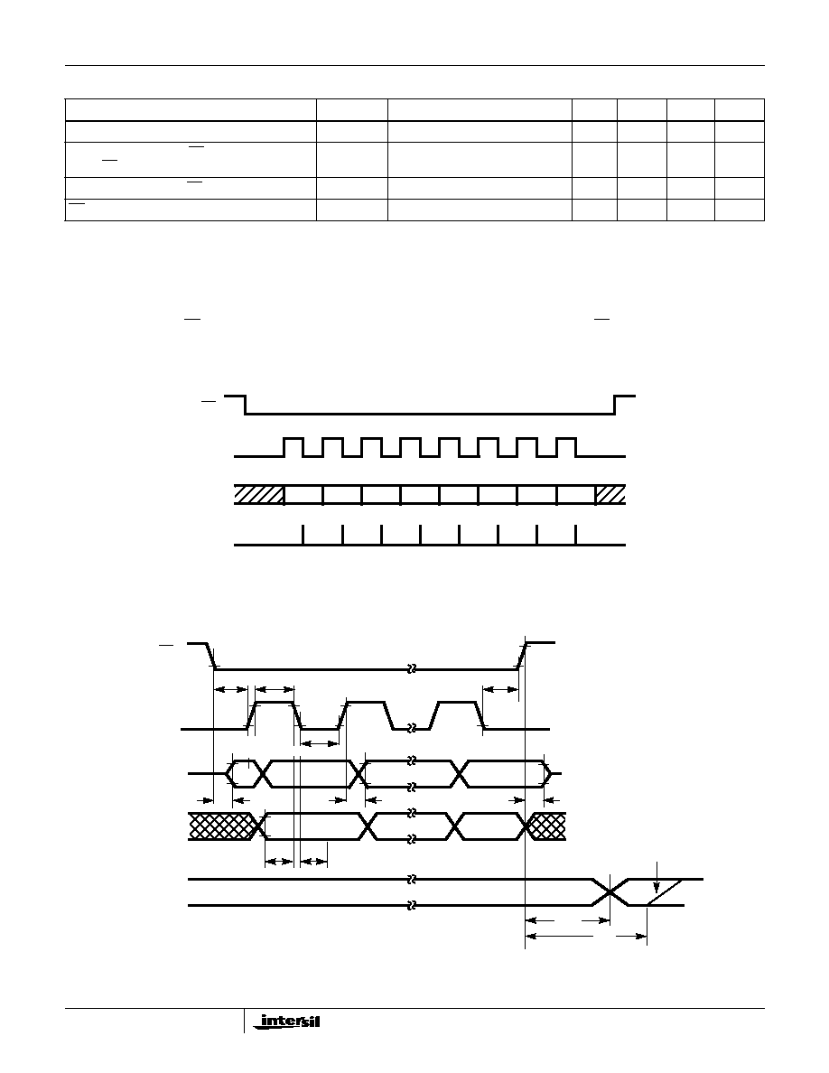
FIGURE 1A. DATA AND CLOCK TIMING DIAGRAM
FIGURE 1B. SPI TIMING DIAGRAM
CE
SCK
MSB 6 5 4 3 2 1 LSB
(CPOL = 0, CPHA = 1)
INTERNAL STROBE FOR DATA CAPTURE
CE
(INPUT)
SCK
(INPUT)
MISO
(OUTPUT)
MOSI
(INPUT)
DRIVER
OUTPUT
HIGH
Z
LAST BIT
TRANSMITTED
D7O
D6O
D0O
D7I
D6I
D0I
OLD
FAULT-INDUCED
TURN-OFF
t
DON
t
DOFF
t
DF
t
DIS
t
V
t
LAG
t
H
t
SU
t
WSCKL
t
WSCKH
t
LEAD
t
EN
NEW
HIP0045
4-6
Signal Pin Descriptions
Power Output Drivers, OUT0 - OUT7 - The input and
output bits corresponding to Output 0 thru Output 7 are
transmitted and received most significant bit (MSB) first via
the SPI bus. Outputs OUT0 - 5 are provided with over-
current shutdown. Current Limiting and Thermal Shutdown
are provided on OUT6, 7 for application use as Lamp
Drivers. After a fault shutdown, the control lines remain
active. The fault latches must be cleared by turning the
output off and on to reset the output to an ON state. OUT1, 2
latches may be cleared by the RESET pin.
RESET - Active low reset input. An internal pull-up is
provided on-chip. When this input line is low, all output
drivers are turned-off and the OUT1, 2 fault latches are
cleared. An internal low voltage reset is ORed with the
RESET input. When V
CC
is less than V
LCC_RST
, the
internal reset is active.
CE - Active low chip enable. The falling edge of CE loads the
shift register with the output status bits. Data is transferred
from the shift register to the outputs on the rising edge of CE.
The output driver for the MISO pin is enabled when CE goes
low. CE must be a logic low prior to the first serial clock (SCK)
and must remain low until after the last (eighth) serial clock
cycle. All eight MOSI bits of input data must be loaded in the
same sequence of SCK clock input. A digital filter is used in
the CE line to insure that 8 (or a multiple of 8) clock cycles
occurs while CE is active low. After SCK is low for a short
period, t
LAG
; CE may be changed from low to high to latch the
input data. A low level on CE also activates an internal disable
circuit used for unlatching output states that are in a fault
mode as sensed by an out of saturation condition. A high on
CE forces MISO to a high impedance state. Also, when CE is
high, the octal driver ignores the SCK and MOSI signals.
IN0, 1 - IN0 and IN1 are Channels 0 and 1 direct parallel
input controls. Refer to `Special Input Conditions for Channel
0, 1` in the following text.
SCK, MISO, MOSI - Refer to the `Serial Peripheral Interface'
(SPI) section in the following text.
Serial Peripheral Interface (SPI)
The Serial Peripheral Interface (SPI) is a serial synchronous
bus for control and data transfers. The Clock (SCK), which is
generated by the microcomputer, is active only during data
transfers. In systems using CDP68HC05 family
microcomputers, the inactive clock polarity is determined by
the CPOL bit in the microcomputer's control register. The
CPOL bit is used in conjunction with the clock phase bit,
CPHA to produce the desired clock data relationship
between the microcomputer and octal driver. The CPHA bit
in general selects the clock edge which captures data and
allows it to change states. For the HIP0045, the CPOL bit
must be set to a logic zero and the CPHA bit to a logic one.
Configured in this manner, MISO (output) data will appear
with every rising edge of the SCK clock pulse, and MOSI
(input) data will be latched into the shift register with every
falling edge of the SCK clock pulse. Also, the steady state
value of the inactive serial clock, SCK, will be at a low level.
Timing diagrams for the serial peripheral interface are shown
in Figure 1.
SPI Signal Descriptions
MOSI (Master Out/Slave In) - Serial data input. Data bytes
are shifted in at this pin, most significant bit (MSB) first. The
data is passed directly to the shift register which in turn
controls the latches and output drivers.
MISO (Master In/Slave Out) - Serial data output. Data bytes
are shifted out at this pin, most significant bit (MSB) first.
This pin is the serial output from the shift register and is
three stated when CE is high. Diagnostic Failure Register
information is given in Tables 6 and 7. Determination of the
fault condition may be done as a software sequence, based
on MOSI data latched into the shift register and subsequent
data clocked out of the MISO pin.
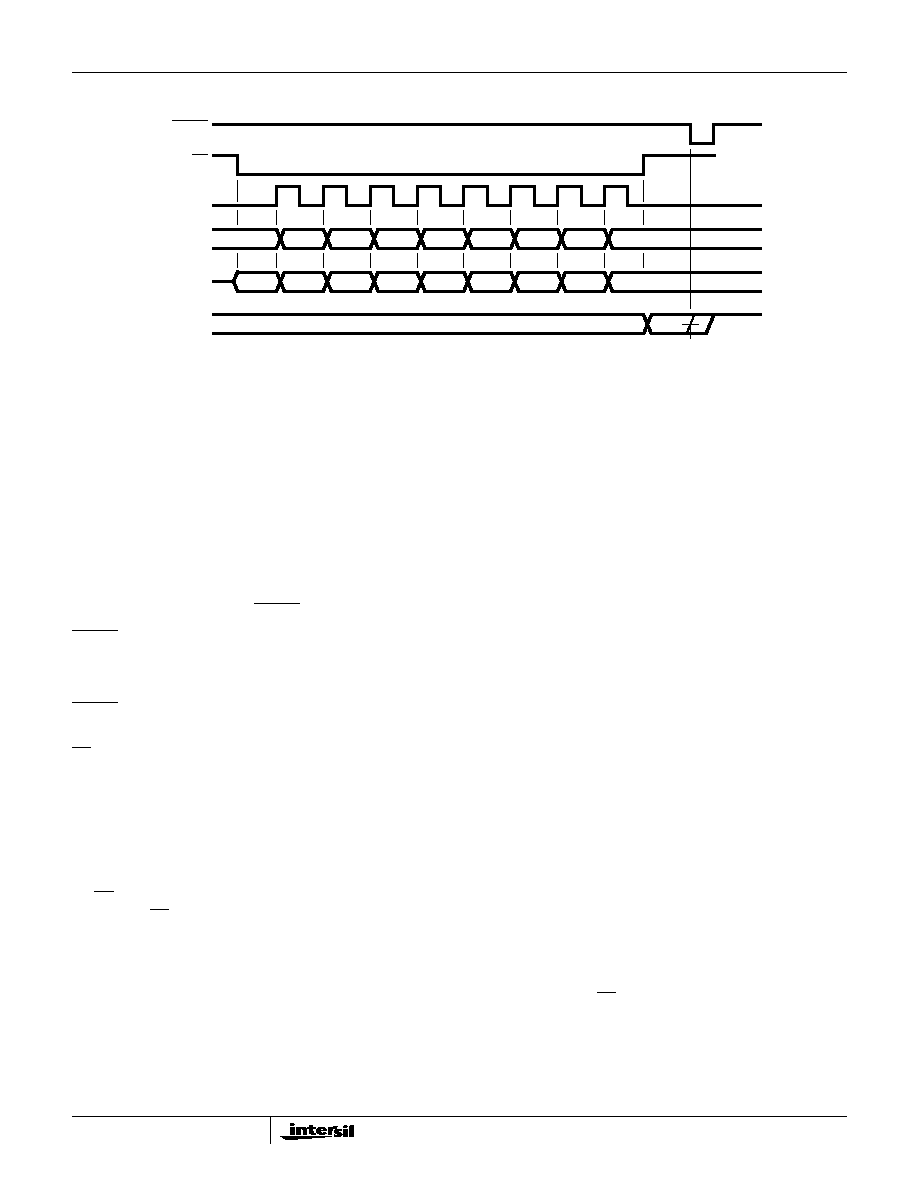
FIGURE 2. BYTE TIMING DIAGRAM WITH ASYNCHRONOUS RESET
Timing Diagrams
(Continued)
OLD
NEW
FAULTS
RESET
7
6
5
4
3
2
1
0
7
6
5
4
3
2
1
0
RESET
CE
SCK
MOSI
MISO
OUTPUTS
HIP0045
4-7
SCK - Serial clock input. The SCK signal clocks the shift
register and new MOSI (input) data will be latched into the
shift register on every falling edge of SCK. The SCK phase
bit, CPHA=1 and the polarity bit, CPOL=0, must be set in the
microcomputer's control register.
Functional Descriptions
The HIP0045 is a low quiescent power, high voltage, high
current, octal, serial low side driver featuring eight channels
of open drain MOS output drivers. Referring to the Detailed
Block Diagram, the drivers have low r
DSON
and low
saturation voltage with over-voltage drain-to-gate zener
clamp circuits. Each output is short circuit protected and
suited for driving resistive or inductive loads such as
solenoids, relays and lamps. Data is transmitted to the
device serially using the Serial Peripheral Interface (SPI)
protocol. Each channel is independently controlled by an
output latch and a common RESET line that disables all
eight outputs. Byte timing with asynchronous reset is shown
in Figure 2.
The circuit receives 8-bit serial data by means of the serial input
(MOSI), and stores this data in an internal register to control the
output drivers. The serial output (MISO) provides 8-bit
diagnostic data representing the voltage level at the driver
output. This allows the microcomputer to diagnose the
condition at the output drivers. The device is selected when the
chip enable (CE) line is low. When (CE) is high, the device is
deselected and the serial output (MISO) is placed in a three-
state high impedance mode. The device shifts serial data on
the rising edge of the serial clock (SCK), and latches data on
the falling edge. On the rising edge of chip enable (CE), new
input data from the shift register is latched to control the output
drivers. The falling edge of chip enable (CE) transfers the
output drivers fault information back to the shift register. The
output drivers have low ON voltage at rated current, and are
monitored by a comparator for an out of saturation condition, in
which case the output driver with the fault becomes unlatched
and diagnostic data is sent to the microcomputer via the MISO
line. A typical microcomputer interface circuit is shown in
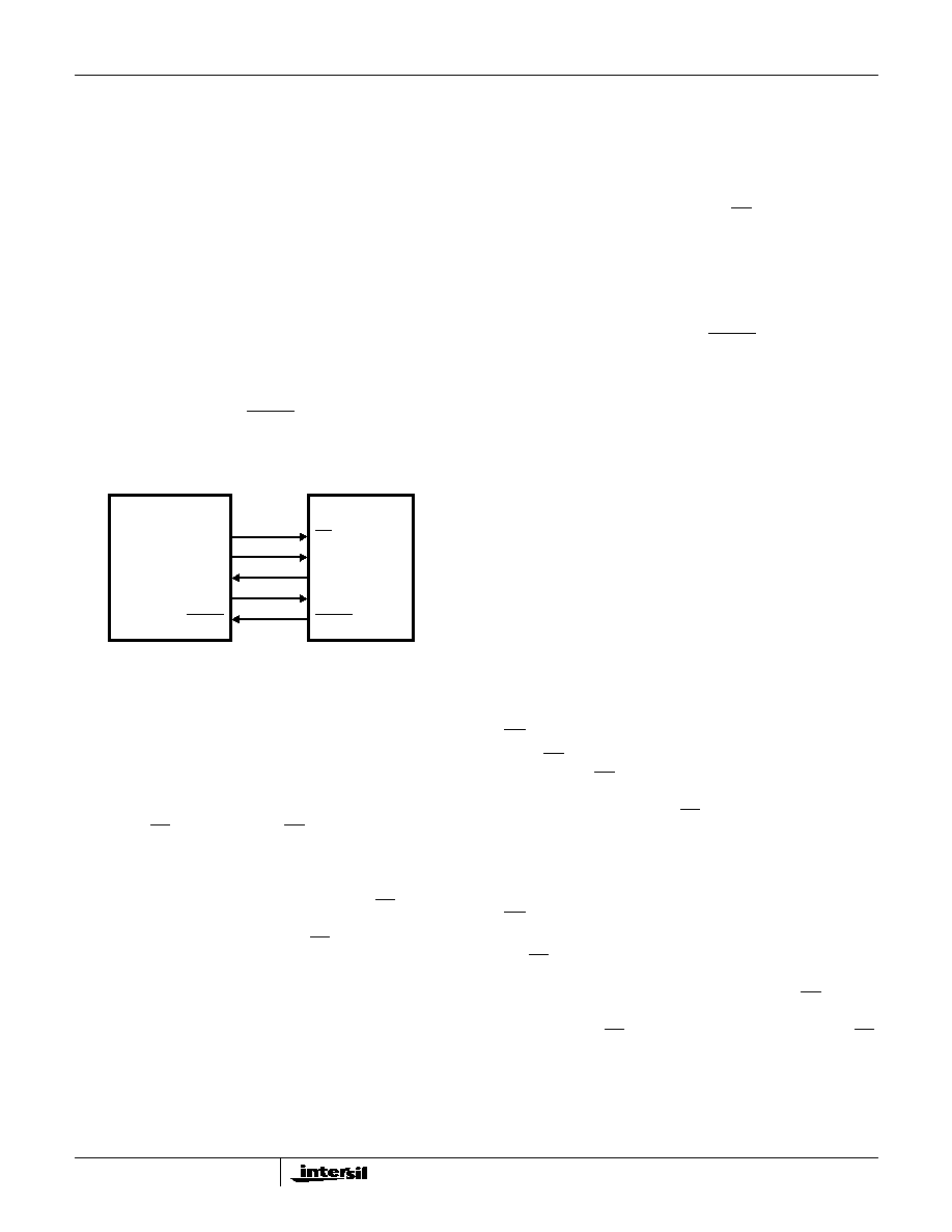
Figure 3.
SPI Shift Register
The SPI shift register has both serial and parallel inputs and
outputs. Serial output and input data are simultaneously
transferred to and from the SPI bus. The serial input data is
parallel latched into the 8-Bit Output Latch of the HIP0045 at
the end of a data transfer. Diagnostic data, Diag0-7 is
transferred to the shift register when CE goes low at the
beginning of a data transfer cycle.
8-Bit Output Latch
The 8-Bit Output Latch is used to control the output drivers.
New serial data is transferred from the shift register to the
8-Bit Output Latch when CE goes high. The 8-Bit Output
Latch is cleared by an active low RESET signal.
Output Drivers
The output drivers provide an active low output of 500mA
nominal with current limiting set to greater than 1.05A to
allow for high inrush currents. In addition, each output is
provided with a voltage drain-to-gate clamp circuit to limit
inductive transients. Each output driver is also monitored by
a comparator for an out of saturation condition. If the output
voltage of an ON output pin exceeds the saturation voltage
limit, a fault latch turns off the output. The threshold
comparators are used to detect shorts to the power supply,
shorts to ground and open loads. Each comparator provides
status data to the shift register for diagnostic feedback. An
internal pull-down current, I
SK
at each output will provide an
indicator for low output voltage if the output is programmed
OFF and the output line is open. Refer to Tables 6 and 7 for
Fault information versus output control and V
REF
. Note that
V
REF
is the out-of-saturation threshold for an ON state.
When the output is switched off and V
REF
is low, an open-
load or ground fault is indicated.
CE High to Low Transition
When CE is low the three-state MISO pin is enabled. On the
falling edge of CE, diagnostic and status data from the
output voltage comparators will be latched into the shift
register. During the time that CE is low, data bytes controlling
the output drivers are shifted in at the MOSI pin most
significant bit (MSB) first. Tables 1, 2 and 3 define the logic
state for control of each output and Table 4 defines the
control bit structure.
CE Low to High Transition
When the last serial data bit has been shifted into the MOSI
pin, CE pin is pulled high to transfer data from the shift register
into the 8-bit parallel output latch to activate the outputs. The
serial clock input pin (SCK) should be low during CE
transitions to avoid false clocking of the shift register. The SCK
input is gated by CE so that the SCK input is ignored when CE
is high.
PORT
MOSI
MISO
SCK
RESET
CE
MOSI
MISO
SCK
RESET
CDP68HC05C4
MICROCOMPUTER
HIP0045
FIGURE 3. TYPICAL MICROCOMPUTER INTERFACE WITH
THE HIP0045
HIP0045
4-8
Detecting Fault Conditions
Fault conditions may be checked as follows: SCK is always
low when CE is changing. When CE goes low, the MISO
output is taken out of the three-state mode and the Output
status information is latched into the shift register. While CE is
low, data bits in the shift register are transferred to the MISO
output on each positive SCK clock transition and data bits
present at the MOSI input are transferred into the shift register
on each negative transition of SCK. To verify Status and
Diagnostic conditions, clock in a new control byte and wait
approximately 150
µ
s to allow the outputs to settle. Clock in
the same control byte and compare this to the data output at
the MISO pin. If there is a disparity, use Tables 5, 6 and 7 to
determine the fault or status condition. (Use Tables 1, 2, 3 and
4 to establish the ON/OFF conditions for each output).
Based on the needs of the application, a software sequence
should be programmed into the microcontroller to set the
corrective action of each fault condition.
Special Conditions for Channel 0, 1
Referring to the Detailed Block Diagram, Channel's 0, 1 are
configured to externally provide control of the ON/OFF state.
The inputs, IN0 and IN1, are ORed with the SPI ON/OFF
control bit. In this configuration with IN0 and IN1 high, SPI
control latches Diag0 and Diag1 as status bits. When the IN0
and IN1 inputs are active, a fault condition is detected by a
comparison of IN0 and IN1 to OUT0 and OUT1 respectively
causing the Fault Detector to latch a fault bit. The resulting
Fault output is latched as diagnostic bit, Diag0 or Diag1. The
Diag0 and Diag1 outputs give the status or fault condition of
the output drivers as shown in Table 6. Fault detection is
disabled during switching/settling time.
The Diag0 and Diag1 bits from Channel 0 and 1 respectively
indicate a fault when the FAULT BIT is Low, given IN1 and
IN0 control. Otherwise Diag0 and Diag1 are status bits when
controlled by the SPI input. Note that the SPI Bit, given in
Tables 1 and 2 overrides the ON state control from IN0
and IN1.
TABLE 5. DIAGNOSTIC FAILURE REGISTER STRUCTURE
Diag1
Diag3
Diag5
Diag7
Diag0
Diag2
Diag4
Diag6
(D7O)
(D6O)
(D5O)
(D4O)
(D3O)
(D2O)
(D1O)
(D0O)
MSB
LSB
NOTE:
10. The Diagnostic Failure Register bits Diag0 -7 have the same
order as the Control Register bits Q0 - 7 as defined in Table 4.
Data bits D0O - D7O give the MISO SPI serial output flow
sequence.
TABLE 6. DEFINITION OF Diag0, 1 FAULT BITS FOR OUT0,
1 IN PARALLEL-CONTROLLED MODE
OUTPUT
STATE
V
REF
STATUS
FAULT
BIT
FAULT
MODE
OFF
>V
REF
H
No Fault
OFF
<V
REF
L
Open Load or GND Short
ON
<V
REF
H
No Fault
ON
>V
REF
L
Short to V
BATT
TABLE 7. DEFINITION OF Diag0-7 STATUS BITS FOR OUT0-7
OUTPUT
STATE
V
REF
STATUS
STATUS
BIT
FAULT
MODE
OFF
>V
REF
H
No Fault
OFF
<V
REF
L
Open Load or GND Short
ON
<V
REF
L
No Fault
ON
>V
REF
H
Short to V
BATT
(Chan. 0-7);
or Over-Temperature Fault
(Chan. 6, 7)
NOTES:
11. For Channel 0 (Diag0) and Channel 1 (Diag1):
Fault Bit High = No Fault; Fault Bit Low = Fault Occurred.
12. V
REF
is the threshold reference level for detecting an Open Load.
Refer to the Electrical Specification for the V
REF
voltage level.
0.1
1
10
100
10
100
1000
TIME (ms)
ENERGY (mJ)
SAFE OPERATING AREA
BELOW LINE
FIGURE 4. MAXIMUM SINGLE PULSE ENERGY SAFE
OPERATING AREA FOR EACH CLAMPED
OUTPUT DRIVER, T
A
= 25
o
C
HIP0045
4-9
HIP0045
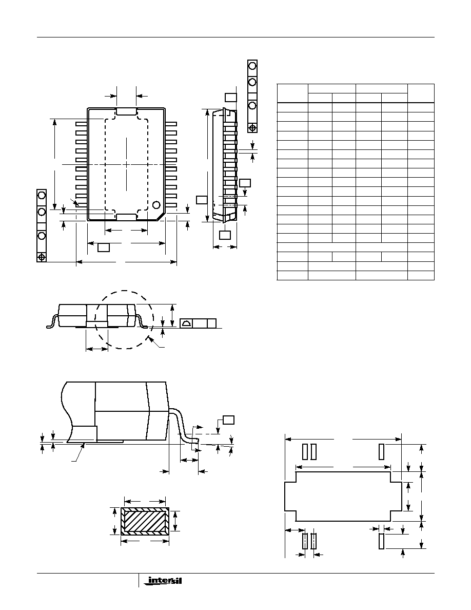
Power Small Outline Plastic Package (PSOP)
E2
1
2
3
D2
E
1.10 MAX. X 45
o
2 PLACES
2 PLA
CES
D1
0.25
CB
M
A
S
S
E1
-B-
E3
N
(D
A
TUM
PIN 1
PLANE A)
MARKER
D
b
SEATING
A
0.25
CA
M
B
S
S
-C-
-A-
A1
SEE DETAIL "A"
A2
C
0.10
SECTION "B-B"
b
b
1
c
1
c
3.10 REF.
SEATING
PLANE
DETAIL "A"
B
B
0-8
o
1.60 REF.
GAUGE
L
0.15
REF.
A3
HEAT
PLANE
SLUG
L1
PLANE
-H-
e
M20.433
20 LEAD POWER SMALL OUTLINE PLASTIC
PACKAGE
SYMBOL
INCHES
MILLIMETERS
NOTES
MIN
MAX
MIN
MAX
A
0.122
0.142
3.10
3.60
-
A1
0.004
0.012
0.10
0.30
-
A2
0.118
0.130
3.00
3.30
-
A3
0.000
0.004
0.00
0.10
-
b
0.016
0.021
0.40
0.53
6, 7
b1
0.016
0.020
0.40
0.50
6, 7
c
0.009
0.013
0.23
0.32
7
c1
0.009
0.011
0.23
0.29
7
D
0.622
0.630
15.80
16.00
3
D1
0.496
0.512
12.60
13.00
-
D2
-
0.043
-
1.10
-
E
0.547
0.571
13.90
14.50
-
E1
0.429
0.437
10.90
11.10
4
E2
-
0.114
-
2.90
-
E3
0.228
0.244
5.80
6.20
-
e
0.050 BSC
1.27 BSC
-
L
0.031
0.043
0.80
1.10
5
L1
0.014 BSC
0.35 BSC
-
N
20
20
-
Rev. 0 3/96
NOTES:
1. Dimensioning and tolerancing per ANSI Y14.5M-1982.
2. "C" is a reference datum. Seating plane is defined by
lead tips only.
3. Dimension D does not include mold flash, protrusions
or gate burrs. Mold flash, protrusions or gate burrs
shall not exceed 0.15 per side. D measured at -H-.
4. Dimension E1 does not include interlead flash or pro-
trusion. Interlead flash or protrusion shall not exceed
0.15 per side. E1 measured at -H-.
5. Dimension "L" is the length of terminal for soldering to
a substrate.
6. The lead width dimension does not include dambar
protrusion. Allowable dambar protrusion shall be
0.08mm total in excess of the lead width dimension at
maximum material condition.
7. Section "B-B" to be determined at 0.10mm to 0.25mm
from the lead tip.
8. Controlling dimension: MILLIMETER.
9. Dimensions conform with JEDEC Outline MO-166AA
Issue B.
17.15
LAND PATTERN
N
1
13.92
4.22
1.52
0.71
2.87
e
7.26
4.09
2.21
4.09

4-10
All Intersil semiconductor products are manufactured, assembled and tested under ISO9000 quality systems certification.
Intersil semiconductor products are sold by description only. Intersil Corporation reserves the right to make changes in circuit design and/or specifications at any time with-
out notice. Accordingly, the reader is cautioned to verify that data sheets are current before placing orders. Information furnished by Intersil is believed to be accurate and
reliable. However, no responsibility is assumed by Intersil or its subsidiaries for its use; nor for any infringements of patents or other rights of third parties which may result
from its use. No license is granted by implication or otherwise under any patent or patent rights of Intersil or its subsidiaries.
For information regarding Intersil Corporation and its products, see web site http://www.intersil.com
Sales Office Headquarters
NORTH AMERICA
Intersil Corporation
P. O. Box 883, Mail Stop 53-204
Melbourne, FL 32902
TEL: (407) 724-7000
FAX: (407) 724-7240
EUROPE
Intersil SA
Mercure Center
100, Rue de la Fusee
1130 Brussels, Belgium
TEL: (32) 2.724.2111
FAX: (32) 2.724.22.05
ASIA
Intersil (Taiwan) Ltd.
7F-6, No. 101 Fu Hsing North Road
Taipei, Taiwan
Republic of China
TEL: (886) 2 2716 9310
FAX: (886) 2 2715 3029
HIP0045