1
Æ
February 2003
HIP4080A
80V/2.5A Peak, High Frequency Full Bridge
FET Driver
The HIP4080A is a high frequency, medium voltage Full
Bridge N-Channel FET driver IC, available in 20 lead plastic
SOIC and DIP packages. The HIP4080A includes an input
comparator, used to facilitate the "hysteresis" and PWM
modes of operation. Its HEN (high enable) lead can force
current to freewheel in the bottom two external power
MOSFETs, maintaining the upper power MOSFETs off.
Since it can switch at frequencies up to 1MHz, the HIP4080A
is well suited for driving Voice Coil Motors, switching power
amplifiers and power supplies.
HIP4080A can also drive medium voltage brush motors, and
two HIP4080As can be used to drive high performance
stepper motors, since the short minimum "on-time" can
provide fine micro-stepping capability.
Short propagation delays of approximately 55ns maximizes
control loop crossover frequencies and dead-times which
can be adjusted to near zero to minimize distortion, resulting
in precise control of the driven load.
The similar HIP4081A IC allows independent control of all 4
FETs in an Full Bridge configuration.
The Application Note for the HIP4080A is AN9404.
Features
∑ Drives N-Channel FET Full Bridge Including High Side
Chop Capability
∑ Bootstrap Supply Max Voltage to 95VDC
∑ Drives 1000pF Load at 1MHz in Free Air at +50
o
C with
Rise and Fall Times of Typically 10ns
∑ User-Programmable Dead Time
∑ Charge-Pump and Bootstrap Maintain Upper Bias
Supplies
∑ DIS (Disable) Pin Pulls Gates Low
∑ Input Logic Thresholds Compatible with 5V to 15V Logic
Levels
∑ Very Low Power Consumption
∑ Undervoltage Protection
Applications
∑ Medium/Large Voice Coil Motors
∑ Full Bridge Power Supplies
∑ Switching Power Amplifiers
∑ High Performance Motor Controls
∑ Noise Cancellation Systems
∑ Battery Powered Vehicles
∑ Peripherals
∑ U.P.S.
Pinout
Ordering Information
PART
NUMBER
TEMPERATURE
RANGE
PACKAGE
HIP4080AIP
-40
o
C to +85
o
C
20 Lead Plastic DIP
HIP4080AIB -40
o
C to +85
o
C
20 Lead Plastic SOIC (W)
11
12
13
14
15
16
17
18
20
19
10
9
8
7
6
5
4
3
2
1
BHB
HEN
DIS
V
SS
OUT
IN+
HDEL
IN-
LDEL
AHB
BHO
BLO
BLS
V
DD
BHS
V
CC
ALS
ALO
AHS
AHO
HIP4080A
(PDIP, SOIC)
TOP VIEW
Data Sheet
FN3658.5
CAUTION: These devices are sensitive to electrostatic discharge; follow proper IC Handling Procedures.
1-888-INTERSIL or 321-724-7143
|
Intersil (and design) is a registered trademark of Intersil Americas Inc.
Copyright © Intersil Americas Inc. 2003. All Rights Reserved
All other trademarks mentioned are the property of their respective owners.

2
HIP4080A
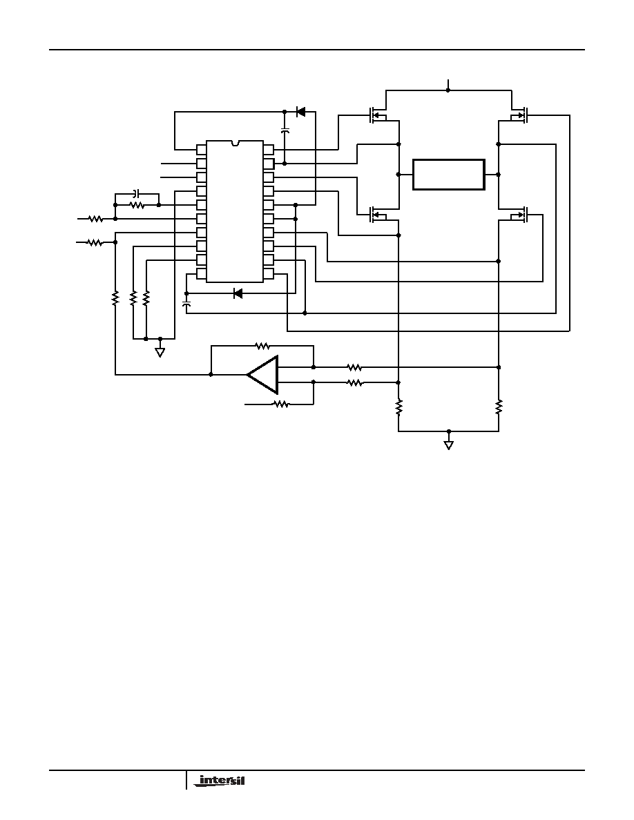
Application Block Diagram
Functional Block Diagram
(1/2 HIP4080A)
80V
GND
HIP4080A
GND
12V
LOAD
BHO
BHS
BLO
ALO
AHS
AHO
IN-
IN+
DIS
HEN
CHARGE
PUMP
V
DD
HEN
DIS
OUT
IN+
IN
_
HDEL
LDEL
V
SS
TURN-ON
DELAY
+
-
TURN-ON
DELAY
DRIVER
DRIVER
AHB
AHO
AHS
V
CC
ALO
ALS
C
BF
TO V
DD
(PIN 16)
C
BS
D
BS
HIGH VOLTAGE BUS
80VDC
+12VDC
LEVEL SHIFT
AND LATCH
14
10
11
12
15
13
16
2
3
5
6
7
8
9
4
BIAS
SUPPLY
UNDER-
VOLTAGE
3
Typical Application (Hysteresis Mode Switching)
6V
80V
12V
12V
DIS
IN
GND
6V
GND
+
-
11
12
13
14
15
16
17
18
20
19
10
9
8
7
6
5
4
3
2
1 BHB
HEN
DIS
V
SS
OUT
IN+
HDEL
IN-
LDEL
AHB
BHO
BLO
BLS
V
DD
BHS
V
CC
ALS
ALO
AHS
AHO
LOAD
H
I
P4
080A/
H
IP
4080
HIP4080A
4
HIP4080A
Absolute Maximum Ratings
Thermal Information
Supply Voltage, V
DD
and V
CC
. . . . . . . . . . . . . . . . . . . . -0.3V to 16V
Logic I/O Voltages . . . . . . . . . . . . . . . . . . . . . . . -0.3V to V
DD
+0.3V
Voltage on AHS, BHS. . . . -6.0V (Transient) to 80V (25
o
C to 125
o
C)
Voltage on AHS, BHS. . . . -6.0V (Transient) to 70V (-55
o
C to 125
o
C)
Voltage on ALS, BLS . . . . . . . -2.0V (Transient) to +2.0V (Transient)
Voltage on AHB, BHB. . . . . . . . . V
AHS, BHS
-0.3V to V
AHS, BHS
+V
DD
Voltage on ALO, BLO . . . . . . . . . . . . . .V
ALS, BLS
-0.3V to V
CC
+0.3V
Voltage on AHO, BHO . . . . . . . .V
AHS, BHS
-0.3V to V
AHB, BHB
+0.3V
Input Current, HDEL and LDEL . . . . . . . . . . . . . . . . . . -5mA to 0mA
Phase Slew Rate . . . . . . . . . . . . . . . . . . . . . . . . . . . . . . . . . . 20V/ns
NOTE: All Voltages relative to V
SS
, unless otherwise specified.
Thermal Resistance
. . . . . . . . . . . . . . . . . . . . . . . . . . . . . . . . . . . . . . .
JA
SOIC Package. . . . . . . . . . . . . . . . . . . . . . . . . . . . . . . . . +85
o
C/W
DIP Package . . . . . . . . . . . . . . . . . . . . . . . . . . . . . . . . . . +75
o
C/W
Maximum Power Dissipation at +85
o
C
SOIC Package. . . . . . . . . . . . . . . . . . . . . . . . . . . . . . . . . . 470mW
DIP Package . . . . . . . . . . . . . . . . . . . . . . . . . . . . . . . . . . . 530mW
Storage Temperature Range. . . . . . . . . . . . . . . . . . -65
o
C to +150
o
C
Operating Max. Junction Temperature . . . . . . . . . . . . . . . . . +125
o
C
Lead Temperature (Soldering 10s) . . . . . . . . . . . . . . . . . . . . +300
o
C
(For SOIC - Lead Tips Only)
Operating Conditions
Supply Voltage, V
DD
and V
CC
. . . . . . . . . . . . . . . . . . +9.5V to +15V
Voltage on ALS, BLS . . . . . . . . . . . . . . . . . . . . . . . . . -1.0V to +1.0V
Voltage on AHB, BHB. . . . . . . . . . V
AHS, BHS
+5V to V
AHS, BHS
+15V
Input Current, HDEL and LDEL . . . . . . . . . . . . . . . .-500
µ
A to -50
µ
A
Operating Ambient Temperature Range . . . . . . . . . -40
o
C to +85
o
C
CAUTION: Stresses above those listed in "Absolute Maximum Ratings" may cause permanent damage to the device. This is a stress only rating and operation of the
device at these or any other conditions above those indicated in the operational sections of this specification is not implied.
Electrical Specifications
V
DD
= V
CC
= V
AHB
= V
BHB
= 12V, V
SS
= V
ALS
= V
BLS
= V
AHS
= V
BHS
= 0V, R
HDEL
= R
LDEL
= 100K, and
T
A
= +25
o
C, Unless Otherwise Specified
PARAMETERS
SYMBOL
TEST CONDITIONS
T
J
= +25
o
C
T
J
= - 40
o
C
TO +125
o
C
UNITS
MIN
TYP
MAX
MIN
MAX
SUPPLY CURRENTS AND CHARGE PUMPS
V
DD
Quiescent Current
I
DD
IN- = 2.5V, Other Inputs = 0V
8
11
14
7
14
mA
V
DD
Operating Current
I
DDO
Outputs switching f = 500kHz, No Load
9
12
15
8
15
mA
V
CC
Quiescent Current
I
CC
IN- = 2.5V, Other Inputs = 0V,
I
ALO
= I
BLO
= 0
-
25
80
-
100
µ
A
V
CC
Operating Current
I
CCO
f = 500kHz, No Load
1
1.25
2.0
0.8
3
mA
AHB, BHB Quiescent Current -
Qpump Output Current
I
AHB
, I
BHB
IN- = 2.5V, Other Inputs = 0V, I
AHO
=
I
BHO
= 0, V
DD
= V
CC
=V
AHB
= V
BHB
= 10V
-50
-25
-11
-60
-10
µ
A
AHB, BHB Operating Current
I
AHBO
, I
BHBO
f = 500kHz, No Load
0.62
1.2
1.5
0.5
1.9
mA
AHS, BHS, AHB, BHB Leakage Current
I
HLK
V
BHS
= V
AHS
= 80V,
V
AHB
= V
BHB
= 93V
-
0.02
1.0
-
10
µ
A
AHB-AHS, BHB-BHS Qpump
Output Voltage
V
AHB
- V
AHS
V
BHB
- V
BHS
I
AHB
= I
AHB
= 0, No Load
11.5
12.6
14.0
10.5
14.5
V
INPUT COMPARATOR PINS: IN+, IN-, OUT
Offset Voltage
V
OS
Over Common Mode Voltage Range
-10
0
+10
-15
+15
mV
Input Bias Current
I
IB
0
0.5
2
0
4
µ
A
Input Offset Current
I
OS
-1
0
+1
-2
+2
µ
A
Input Common Mode Voltage Range
CMVR
1
-
V
DD
-1.5
1
V
DD
-1.5
V
Voltage Gain
AVOL
10
25
-
10
-
V/mV
OUT High Level Output Voltage
V
OH
IN+ > IN-, I
OH
= -250
µ
A
V
DD
-0.4
-
-
V
DD
- 0.5
-
V
OUT Low Level Output Voltage
V
OL
IN+ < IN-, I
OL
= +250
µ
A
-
-
0.4
-
0.5
V
Low Level Output Current
I
OL
V
OUT
= 6V
6.5
14
19
6
20
mA
High Level Output Current
I
OH
V
OUT
= 6V
-17
-10
-3
-20
-2.5
mA
HIP4080A
5
HIP4080A
INPUT PINS: DIS
Low Level Input Voltage
V
IL
Full Operating Conditions
-
-
1.0
-
0.8
V
High Level Input Voltage
V
IH
Full Operating Conditions
2.5
-
-
2.7
-
V
Input Voltage Hysteresis
-
35
-
-
-
mV
Low Level Input Current
I
IL
V
IN
= 0V, Full Operating Conditions
-130
-100
-75
-135
-65
µ
A
High Level Input Current
I
IH
V
IN
= 5V, Full Operating Conditions
-1
-
+1
-10
+10
µ
A
INPUT PINS: HEN
Low Level Input Voltage
V
IL
Full Operating Conditions
-
-
1.0
-
0.8
V
High Level Input Voltage
V
IH
Full Operating Conditions
2.5
-
-
2.7
-
V
Input Voltage Hysteresis
-
35
-
-
-
mV
Low Level Input Current
I
IL
V
IN
= 0V, Full Operating Conditions
-260
-200
-150
-270
-130
µ
A
High Level Input Current
I
IH
V
IN
= 5V, Full Operating Conditions
-1
-
+1
-10
+10
µ
A
TURN-ON DELAY PINS: LDEL AND HDEL
LDEL, HDEL Voltage
V
HDEL,
V
I
HDEL
= I
LDEL
= -100
µ
A
4.9
5.1
5.3
4.8
5.4
V
GATE DRIVER OUTPUT PINS: ALO, BLO, AHO, AND BHO
Low Level Output Voltage
V
OL
I
OUT
= 100mA
0.7
0.85
1.0
0.5
1.1
V
High Level Output Voltage
V
CC
- V
OH
I
OUT
= -100mA
0.8
0.95
1.1
0.5
1.2
V
Peak Pullup Current
I
O
+
V
OUT
= 0V
1.7
2.6
3.8
1.4
4.1
A
Peak Pulldown Current
I
O
-
V
OUT
= 12V
1.7
2.4
3.3
1.3
3.6
A
Under Voltage, Rising Threshold
UV+
8.1
8.8
9.4
8.0
9.5
V
Under Voltage, Falling Threshold
UV-
7.6
8.3
8.9
7.5
9.0
V
Under Voltage, Hysteresis
HYS
0.25
0.4
0.65
0.2
0.7
V
Electrical Specifications
V
DD
= V
CC
= V
AHB
= V
BHB
= 12V, V
SS
= V
ALS
= V
BLS
= V
AHS
= V
BHS
= 0V, R
HDEL
= R
LDEL
= 100K, and
T
A
= +25
o
C, Unless Otherwise Specified (Continued)
PARAMETERS
SYMBOL
TEST CONDITIONS
T
J
= +25
o
C
T
J
= - 40
o
C
TO +125
o
C
UNITS
MIN
TYP
MAX
MIN
MAX
Switching Specifications
V
DD
= V
CC
= V
AHB
= V
BHB
= 12V, V
SS
= V
ALS
= V
BLS
= V
AHS
= V
BHS
= 0V, R
HDEL
= R
LDEL
= 10K,
C
L
= 1000pF, and T
A
= +25
o
C, Unless Otherwise Specified
PARAMETERS
SYMBOL
TEST CONDITIONS
T
J
= +25
o
C
T
J
= - 40
o
C
TO +125
o
C
UNITS
MIN
TYP
MAX
MIN
MAX
Lower Turn-off Propagation Delay (IN+/IN- to ALO/BLO)
T
LPHL
-
40
70
-
90
ns
Upper Turn-off Propagation Delay (IN+/IN- to AHO/BHO)
T
HPHL
-
50
80
-
110
ns
Lower Turn-on Propagation Delay (IN+/IN- to ALO/BLO)
T
LPLH
-
40
70
-
90
ns
Upper Turn-on Propagation Delay (IN+/IN- to AHO/BHO)
T
HPLH
-
70
110
-
140
ns
Rise Time
T
R
-
10
25
-
35
ns
Fall Time
T
F
-
10
25
-
35
ns
Turn-on Input Pulse Width
T
PWIN-ON
50
-
-
50
-
ns
Turn-off Input Pulse Width
T
PWIN-OFF
40
-
-
40
-
ns
Disable Turn-off Propagation Delay
(DIS - Lower Outputs)
T
DISLOW
-
45
75
-
95
ns
6
Disable Turn-off Propagation Delay
(DIS - Upper Outputs)
T
DISHIGH
-
55
85
-
105
ns
Disable to Lower Turn-on Propagation Delay
(DIS - ALO and BLO)
T
DLPLH
-
45
70
-
90
ns
Refresh Pulse Width (ALO and BLO)
T
REF-PW
240
380
500
200
600
ns
Disable to Upper Enable (DIS - AHO and BHO)
T
UEN
-
480
630
-
750
ns
HEN-AHO, BHO Turn-off, Propagation Delay
T
HEN-PHL
R
HDEL
= R
LDEL
= 10K
-
40
70
-
90
ns
HEN-AHO, BHO Turn-on, Propagation Delay
T
HEN-PLH
R
HDEL
= R
LDEL
= 10K
-
60
90
-
110
ns
Switching Specifications
V
DD
= V
CC
= V
AHB
= V
BHB
= 12V, V
SS
= V
ALS
= V
BLS
= V
AHS
= V
BHS
= 0V, R
HDEL
= R
LDEL
= 10K,
C
L
= 1000pF, and T
A
= +25
o
C, Unless Otherwise Specified (Continued)
PARAMETERS
SYMBOL
TEST CONDITIONS
T
J
= +25
o
C
T
J
= - 40
o
C
TO +125
o
C
UNITS
MIN
TYP
MAX
MIN
MAX
TRUTH TABLE
INPUT
OUTPUT
IN+ > IN-
HEN
U/V
DIS
ALO
AHO
BLO
BHO
X
X
X
1
0
0
0
0
0
0
0
0
1
0
0
0
1
1
0
0
0
1
1
0
0
1
0
0
1
0
0
1
1
0
0
0
0
0
1
0
X
X
1
X
0
0
0
0
HIP4080A
7
Pin Descriptions
PIN
NUMBER
SYMBOL
DESCRIPTION
1
BHB
B High-side Bootstrap supply. External bootstrap diode and capacitor are required. Connect cathode of bootstrap
diode and positive side of bootstrap capacitor to this pin. Internal charge pump supplies 30
µ
A out of this pin to
maintain bootstrap supply. Internal circuitry clamps the bootstrap supply to approximately 12.8V.
2
HEN
High-side Enable input. Logic level input that when low overrides IN+/IN- (Pins 6 and 7) to put AHO and BHO drivers
(Pins 11 and 20) in low output state. When HEN is high AHO and BHO are controlled by IN+/IN- inputs. The pin can
be driven by signal levels of 0V to 15V (no greater than V
DD
).
3
DIS
DISable input. Logic level input that when taken high sets all four outputs low. DIS high overrides all other inputs. When
DIS is taken low the outputs are controlled by the other inputs. The pin can be driven by signal levels of 0V to 15V (no
greater than V
DD
).
4
V
SS
Chip negative supply, generally will be ground.
5
OUT
OUTput of the input control comparator. This output can be used for feedback and hysteresis.
6
IN+
Noninverting input of control comparator. If IN+ is greater than IN- (Pin 7) then ALO and BHO are low level outputs
and BLO and AHO are high level outputs. If IN+ is less than IN- then ALO and BHO are high level outputs and BLO
and AHO are low level outputs. DIS (Pin 3) high level will override IN+/IN- control for all outputs. HEN (Pin 2) low level
will override IN+/IN- control of AHO and BHO. When switching in four quadrant mode, dead time in a half bridge leg
is controlled by HDEL and LDEL (Pins 8 and 9).
7
IN-
Inverting input of control comparator. See IN+ (Pin 6) description.
8
HDEL
High-side turn-on DELay. Connect resistor from this pin to V
SS
to set timing current that defines the turn-on delay of
both high-side drivers. The low-side drivers turn-off with no adjustable delay, so the HDEL resistor guarantees no
shoot-through by delaying the turn-on of the high-side drivers. HDEL reference voltage is approximately 5.1V.
9
LDEL
Low-side turn-on DELay. Connect resistor from this pin to V
SS
to set timing current that defines the turn-on delay of
both low-side drivers. The high-side drivers turn-off with no adjustable delay, so the LDEL resistor guarantees no
shoot-through by delaying the turn-on of the low-side drivers. LDEL reference voltage is approximately 5.1V.
10
AHB
A High-side Bootstrap supply. External bootstrap diode and capacitor are required. Connect cathode of bootstrap
diode and positive side of bootstrap capacitor to this pin. Internal charge pump supplies 30
µ
A out of this pin to
maintain bootstrap supply. Internal circuitry clamps the bootstrap supply to approximately 12.8V.
11
AHO
A High-side Output. Connect to gate of A High-side power MOSFET.
12
AHS
A High-side Source connection. Connect to source of A High-side power MOSFET. Connect negative side of bootstrap
capacitor to this pin.
13
ALO
A Low-side Output. Connect to gate of A Low-side power MOSFET.
14
ALS
A Low-side Source connection. Connect to source of A Low-side power MOSFET.
15
V
CC
Positive supply to gate drivers. Must be same potential as V
DD
(Pin 16). Connect to anodes of two bootstrap diodes.
16
V
DD
Positive supply to lower gate drivers. Must be same potential as V
CC
(Pin 15). De-couple this pin to V
SS
(Pin 4).
17
BLS
B Low-side Source connection. Connect to source of B Low-side power MOSFET.
18
BLO
B Low-side Output. Connect to gate of B Low-side power MOSFET.
19
BHS
B High-side Source connection. Connect to source of B High-side power MOSFET. Connect negative side of bootstrap
capacitor to this pin.
20
BHO
B High-side Output. Connect to gate of B High-side power MOSFET.
HIP4080A
8
HIP4080A
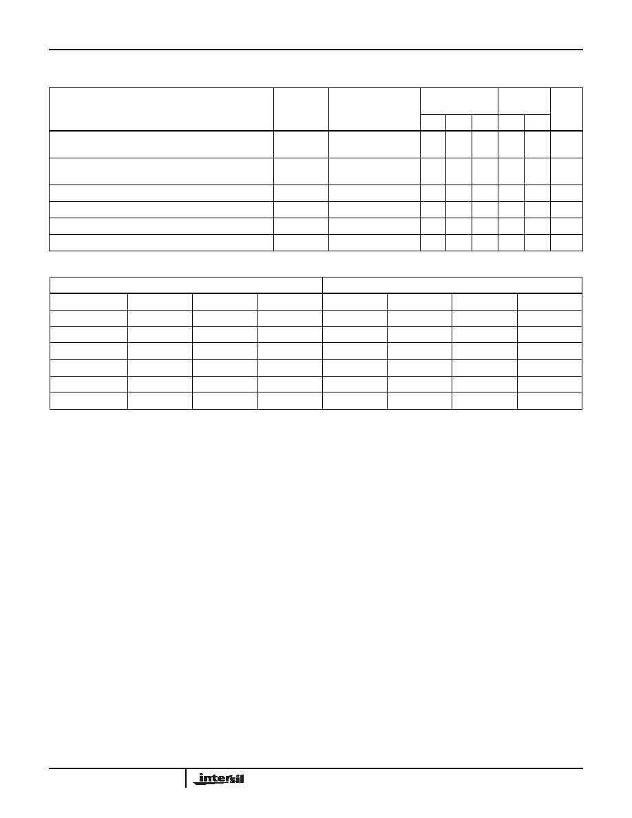
Timing Diagrams
FIGURE 1. BISTATE MODE
FIGURE 2. HIGH SIDE CHOP MODE
FIGURE 3. DISABLE FUNCTION
0
HEN
ALO
AHO
BLO
T
LPHL
T
HPLH
T
R
(10% - 90%)
T
F
(90% - 10%)
T
DT
U/V = DIS
T
HPHL
T
LPLH
T
DT
1
IN+ > IN-
BHO
0
HEN
ALO
AHO
BLO
U/V = DIS
T
HEN-PLH
T
HEN-PHL
IN+ > IN-
BHO
HEN
AHO
BLO
U/V or DIS
T
REF-PW
T
DLPLH
IN+ > IN-
BHO
T
DIS
T
UEN
ALO
9
HIP4080A
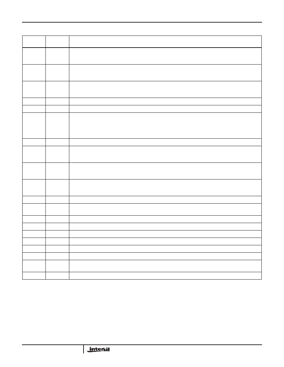
Typical Performance Curves
V
DD
= V
CC
= V
AHB
= V
BHB
= 12V, V
SS
= V
ALS
= V
BLS
= V
AHS
= V
BHS
= 0V, R
HDEL
= R
LDEL
=
100K, and T
A
= +25
o
C, Unless Otherwise Specified
FIGURE 4. QUIESCENT I
DD
SUPPLY CURRENT vs V
DD
SUPPLY VOLTAGE
FIGURE 5. I
DDO
NO-LOAD I
DD
SUPPLY CURRENT vs FRE-
QUENCY (kHz)
FIGURE 6. SIDE A, B FLOATING SUPPLY BIAS CURRENT vs
FREQUENCY (LOAD = 1000pF)
FIGURE 7. I
CCO
, NO-LOAD I
CC
SUPPLY CURRENT vs FRE-
QUENCY (kHz) TEMPERATURE
FIGURE 8. I
AHB
, I
BHB
NO-LOAD FLOATING SUPPLY BIAS
CURRENT vs FREQUENCY
FIGURE 9. COMPARATOR INPUT CURRENT I
L
vs TEMPERA-
TURE AT V
CM
= 5 V
8
10
12
14
2.0
4.0
6.0
8.0
10.0
12.0
14.0
I
DD
SUP
P
L
Y
CU
RRE
N
T
(mA
)
V
DD
SUPPLY VOLTAGE (V)
13
12.5
12.0
11.5
11.0
10.5
10
200
400
600
800
1000
I
DD
S
U
PPL
Y
CURRENT (mA)
SWITCHING FREQUENCY (kHz)
0
100
200
300
400
500
600
700
800
900 1000
0.0
5.0
10.0
15.0
20.0
FL
O
A
TING S
U
PPL
Y
BIAS
CURRENT (
m
A)
SWITCHING FREQUENCY (kHz)
0
100
200
300
400
500
600
700
800
900 1000
0.0
1.0
2.0
3.0
4.0
5.0
I
CC
SUP
P
L
Y
CU
RRE
N
T
(mA)
SWITCHING FREQUENCY (kHz)
+75
o
C
+25
o
C
+125
o
C
-40
o
C
0
o
C
0.5
1
1.5
2
2.5
200
600
800
1000
0
400
FL
O
A
TIN
G
S
U
PPL
Y
BIAS
CURRENT
(m
A)
SWITCHING FREQUENCY (kHz)
-40
-20
0
20
40
60
80
100
120
0.5
1.0
COMP
ARA
T
O
R IN
P
U
T
CURRENT
(
µ
A)
JUNCTION TEMPERATURE (
o
C)
10
HIP4080A
FIGURE 10. DIS LOW LEVEL INPUT CURRENT I
IL
vs TEMPERA-
TURE
FIGURE 11. HEN LOW LEVEL INPUT CURRENT I
IL
vs TEMPER-
ATURE
FIGURE 12. AHB - AHS, BHB - BHS NO-LOAD CHARGE PUMP
VOLTAGE vs TEMPERATURE
FIGURE 13. UPPER DISABLE TURN-OFF PROPAGATION
DELAY T
DISHIGH
vs TEMPERATURE
FIGURE 14. DISABLE TO UPPER ENABLE T
UEN
PROPAGATION
DELAY vs TEMPERATURE
FIGURE 15. LOWER DISABLE TURN-OFF PROPAGATION
DELAY T
DISLOW
vs TEMPERATURE
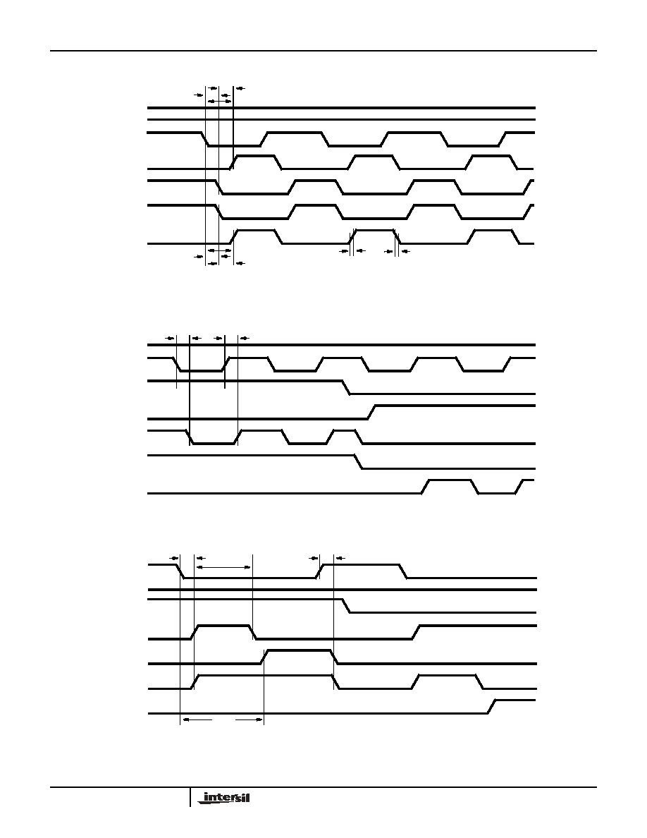
Typical Performance Curves
V
DD
= V
CC
= V
AHB
= V
BHB
= 12V, V
SS
= V
ALS
= V
BLS
= V
AHS
= V
BHS
= 0V, R
HDEL
= R
LDEL
=
100K, and T
A
= +25
o
C, Unless Otherwise Specified (Continued)
-50
-25
0
25
50
75
100
125
-120
-110
-100
-90
L
O
W LEVEL INPUT
CU
RREN
T
(
µ
A)
JUNCTION TEMPERATURE (
o
C)
-40
-20
0
20
40
60
80
100
120
-230
-220
-210
-200
-190
-180
LO
W LEVEL I
N
P
U
T
CURRENT
(
µ
A)
JUNCTION TEMPERATURE (
o
C)
-40
-20
0
20
40
60
80
100
120
10.0
11.0
12.0
13.0
14.0
15.0
NO-LO
AD
F
L
O
A
TING CHARGE
PUMP
V
O
L
T
A
GE
(
V
)
JUNCTION TEMPERATURE (
o
C)
-40
-20
0
20
40
60
80
100
120
30
40
50
60
70
80
P
R
OP
A
G
A
T
ION DELA
Y (ns)
JUNCTION TEMPERATURE (
o
C)
425
450
475
500
525
-50
-25
0
25
50
75
100
125
150
JUNCTION TEMPERATURE (
o
C)
P
R
OP
A
G
A
T
ION DELA
Y (ns)
-40
-20
0
20
40
60
80
100
120
30
40
50
60
70
80
P
R
OP
A
G
A
T
IO
N DEL
A
Y (n
s)
JUNCTION TEMPERATURE (
o
C)
11
HIP4080A
Typical Performance Curves
V
DD
= V
CC
= V
AHB
= V
BHB
= 12V, V
SS
= V
ALS
= V
BLS
= V
AHS
= V
BHS
= 0V, R
HDEL
= R
LDEL
=
10K, and T
A
= +25
o
C, Unless Otherwise Specified
FIGURE 16. T
REF-PW
REFRESH PULSE WIDTH vs TEMPERA-
TURE
FIGURE 17. DISABLE TO LOWER ENABLE TDLPLH PROPAGA-
TION DELAY vs TEMPERATURE
FIGURE 18. UPPER TURN-OFF PROPAGATION DELAY T
HPHL
vs TEMPERATURE
FIGURE 19. UPPER TURN-ON PROPAGATION DELAY THPLH
vs TEMPERATURE
FIGURE 20. LOWER TURN-OFF PROPAGATION DELAY T
LPHL
vs TEMPERATURE
FIGURE 21. LOWER TURN-ON PROPAGATION DELAY T
LPLH
vs
TEMPERATURE
350
375
400
425
450
-50
-25
0
25
50
75
100
125 150
RE
F
R
E
S
H PULSE WIDTH (ns)
JUNCTION TEMPERATURE (
o
C)
-40
-20
0
20
40
60
80
100
120
20
30
40
50
60
70
80
PR
OP
A
G
A
T
ION DELA
Y
(
n
s
)
JUNCTION TEMPERATURE (
o
C)
-40
-20
0
20
40
60
80
100
120
40.0
50.0
60.0
70.0
80.0
90.0
P
R
OP
A
G
A
T
IO
N D
E
LA
Y
(
n
s)
JUNCTION TEMPERATURE (
o
C)
-40
-20
0
20
40
60
80
100
120
40.0
50.0
60.0
70.0
80.0
90.0
P
R
OP
A
G
A
T
IO
N DEL
A
Y (n
s)
JUNCTION TEMPERATURE (
o
C)
-40
-20
0
20
40
60
80
100
120
40.0
50.0
60.0
70.0
80.0
90.0
P
R
OP
A
G
A
T
IO
N DEL
A
Y
(n
s)
JUNCTION TEMPERATURE (
o
C)
-40
-20
0
20
40
60
80
100
120
40.0
50.0
60.0
70.0
80.0
90.0
P
R
OP
A
G
A
T
ION DELA
Y (ns)
JUNCTION TEMPERATURE (
o
C)
12
HIP4080A
Typical Performance Curves
V
DD
= V
CC
= V
AHB
= V
BHB
= 12V, V
SS
= V
ALS
= V
BLS
= V
AHS
= V
BHS
= 0V, R
HDEL
= R
LDEL
=
100K, and T
A
= +25
o
C, Unless Otherwise Specified
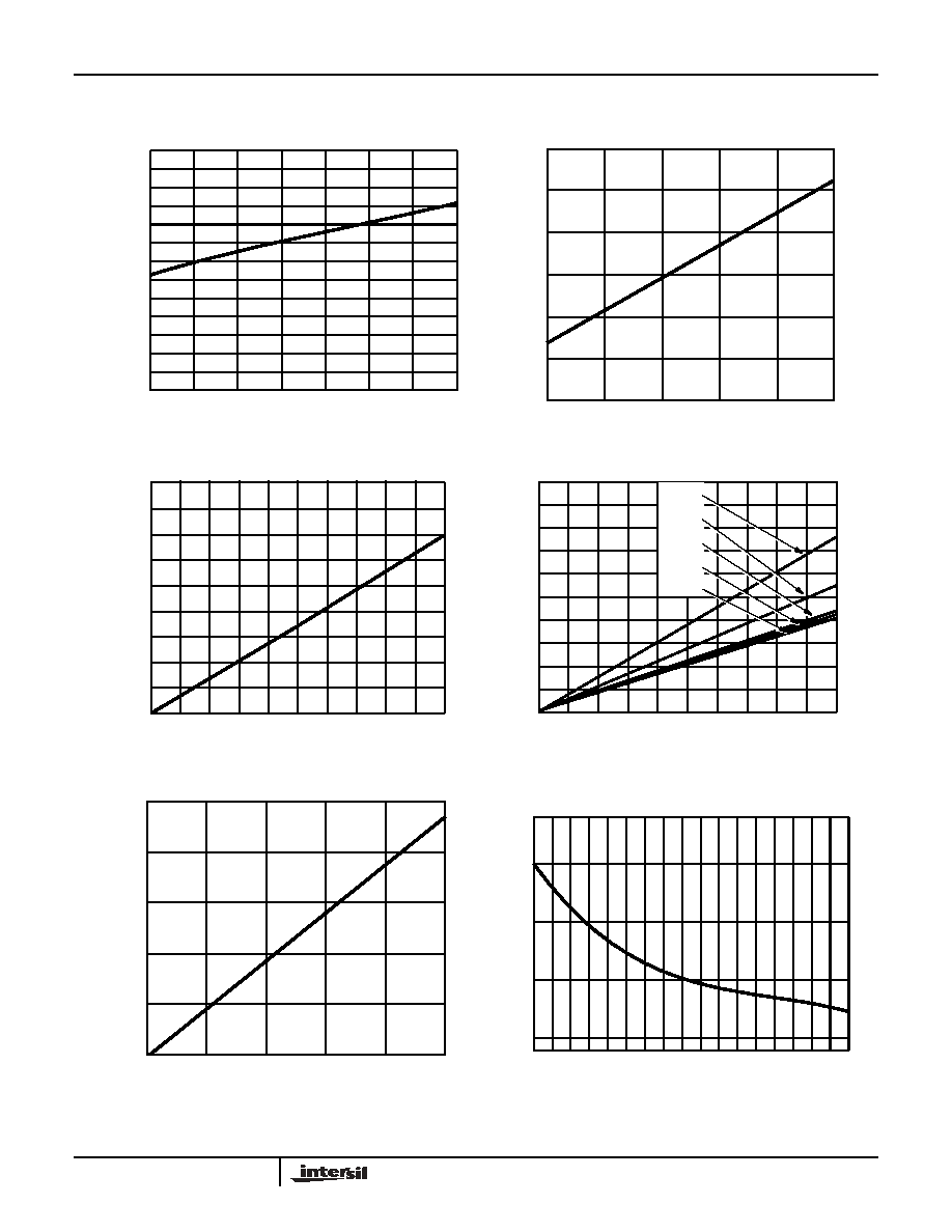
FIGURE 22. GATE DRIVE FALL TIME T
F
vs TEMPERATURE
FIGURE 23. GATE DRIVE RISE TIME T
R
vs TEMPERATURE
FIGURE 24. V
LDEL
, V
HDEL
VOLTAGE vs TEMPERATURE
FIGURE 25. HIGH LEVEL OUTPUT VOLTAGE, V
CC
- V
OH
vs BIAS
SUPPLY AND TEMPERATURE AT 100
µ
A
FIGURE 26. LOW LEVEL OUTPUT VOLTAGE V
OL
vs BIAS
SUPPLY AND TEMPERATURE AT 100
µ
A
FIGURE 27. PEAK PULLDOWN CURRENT I
O-
BIAS SUPPLY
VOLTAGE
-40
-20
0
20
40
60
80
100
120
8.5
9.5
10.5
11.5
12.5
13.5
GA
TE
DRI
VE
F
A
L
L
TI
M
E
(
n
s
)
JUNCTION TEMPERATURE (
o
C)
-40
-20
0
20
40
60
80
100
120
8.5
9.5
10.5
11.5
12.5
13.5
TURN-ON RISE
TIME
(ns
)
JUNCTION TEMPERATURE (
o
C)
-40
-20
0
20
40
60
80
100
120
4.0
4.5
5.0
5.5
6.0
H
D
EL
,
LD
EL IN
P
U
T V
O
L
T
A
G
E
(
V
)
JUNCTION TEMPERATURE (
o
C)
10
12
14
0
250
500
750
1000
1250
1500
V
CC
- V
OH
(mV
)
BIAS SUPPLY VOLTAGE (V)
+75
o
C
+25
o
C
+125
o
C
-40
o
C
0
o
C
12
14
0
250
500
750
1000
1250
1500
V
OL
(mV)
BIAS SUPPLY VOLTAGE (V)
10
+75
o
C
+25
o
C
+125
o
C
-40
o
C
0
o
C
6
7
8
9
10
11
12
13
14
15
16
0.0
0.5
1.0
1.5
2.0
2.5
3.0
3.5
GA
TE DRIV
E
SINK CURR
E
N
T
(A)
V
CC
, V
DD
, V
AHG
, V
BHB
(V)
13
HIP4080A
FIGURE 28. PEAK PULLUP CURRENT I
O+
vs SUPPLY VOLTAGE
FIGURE 29. LOW VOLTAGE BIAS CURRENT I
DD
AND I
CC
(LESS
QUIESCENT COMPONENT) vs FREQUENCY AND
GATE LOAD CAPACITANCE
FIGURE 30. HIGH VOLTAGE LEVEL-SHIFT CURRENT vs
FREQUENCY AND BUS VOLTAGE
FIGURE 31. UNDERVOLTAGE LOCKOUT vs TEMPERATURE
FIGURE 32. MINIMUM DEAD-TIME vs DEL RESISTANCE
Typical Performance Curves
V
DD
= V
CC
= V
AHB
= V
BHB
= 12V, V
SS
= V
ALS
= V
BLS
= V
AHS
= V
BHS
= 0V, R
HDEL
= R
LDEL
=
100K, and T
A
= +25
o
C, Unless Otherwise Specified (Continued)
6
7
8
9
10
11
12
13
14
15
16
0.0
0.5
1.0
1.5
2.0
2.5
3.0
3.5
GA
TE DRIVE
SINK CURRENT
(A)
V
CC
, V
DD
, V
ABH
, V
BHB
(V)
1
10
100
1000
2
5
20
50
500
200
0.1
1
10
100
500
50
5
0.5
200
20
2
0.2
L
O
W V
O
L
T
A
GE BIAS
CUR
RE
NT
(mA)
SWITCHING FREQUENCY (kHz)
3,000
1,000
10,000
100
10
100
1000
20
50
200
500
10
100
1000
20
50
200
500
LEV
E
L-SHIFT CURRENT (
µ
A)
SWITCHING FREQUENCY (kHz)
8.2
8.4
8.6
8.8
9
50
25
0
25
50
75
100
125
150
UV+
UV-
TEMPERATURE (
o
C)
BIAS
S
U
P
P
L
Y
V
O
L
T
A
GE
, V
DD
(V)
10
50
100
150
200
250
0
30
60
90
120
150
HDEL/LDEL RESISTANCE (k
)
DEAD-TIME
(ns
)
14
HIP4080A
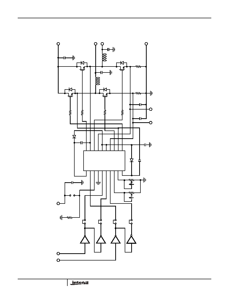
FIGURE 33. HIP4080A EVALUATION PC BOARD SCHEMATIC
1
2
3
1
3
1
3
6
5
1
2
3
2
1
12
13
1
3
10
11
1
2
3
1
2
3
4
5
6
7
8
9
10
11
12
13
14
15
16
17
18
19
20
L1
R21
Q1
Q3
Q4
R22
L2
R23
C1
C3
JMPR1
R24
R30
R31
C2
R34
C4
CR2
CR1
Q2
JMPR5
JMPR3
JMPR2
JMPR4
R33
C5
C6
CX
CY
C8
U1
CW
CW
+
B+
IN2
IN1
BO
OUT/BLI
IN-/AHI
COM
IN+/ALI
+12V
+12V
BLS
AO
HEN/BHI
ALS
CD4069UB
CD4069UB
CD4069UB
CD4069UB
HIP4080A/81A
SECTION
CONTROL LOGIC
POWER SECTION
DRIVER SECTION
AHO
AHB
AHS
LDEL
ALO
HDEL
ALS
IN-/AHI
V
CC
IN+/ALI
V
DD
OUT/BLI
BLS
V
SS
BLO
DIS
BHS
HEN/BHI
BHO
BHB
R29
U2
U2
U2
U2
2
2
2
NOTES:
1. DEVICE CD4069UB PIN 7 = COM. PIN 14 = +12V.
2. COMPONENTS L1, L2, C1, C2, CX, CY, R30, R31, ARE NOT
SUPPLIED. REFER TO APPLICATION NOTE FOR HELP IN
DETERMINING JMPR1 - JMPR4 JUMPER LOCATIONS.
15
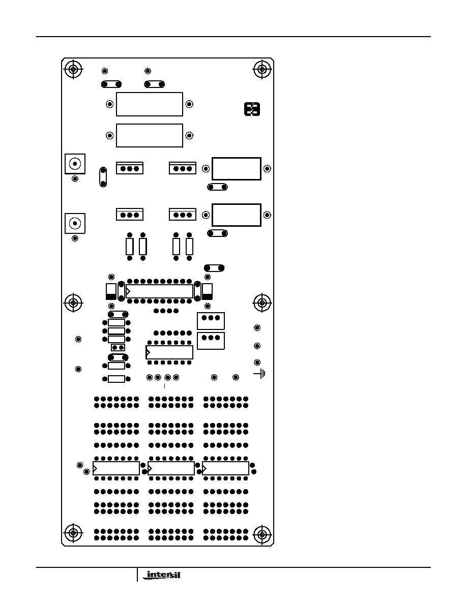
FIGURE 34. HIP4080A EVALUATION BOARD SILKSCREEN
R22
1
Q3
L1
C1
JMPR2
JM
PR
5
R31
R33
CR2
R23
R24
R27
R28
R26
1
Q4
1
Q2
JMPR3
U1
R21
GND
L2
C3
C2
C4
JMPR4
JMPR1
R30
CR1
U2
R34
BO
AO
R32
I
O
C8
R29
C7
C6
C5
CY
CX
1
Q1
COM
+12V
B+
IN1
IN2
AHO
BHO
ALO
BLO
BLS
BLS
LDEL
HDEL
DIS
ALS
ALS
O
+
+
HIP
4080
/81
HIP4080A
16
HIP4080A
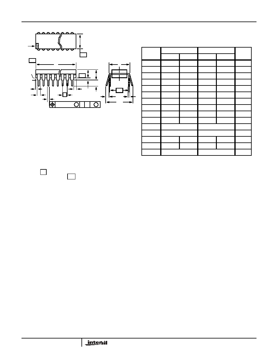
E20.3
(JEDEC MS-001-AD ISSUE D)
20 LEAD DUAL-IN-LINE PLASTIC PACKAGE
SYMBOL
INCHES
MILLIMETERS
NOTES
MIN
MAX
MIN
MAX
A
-
0.210
-
5.33
4
A1
0.015
-
0.39
-
4
A2
0.115
0.195
2.93
4.95
-
B
0.014
0.022
0.356
0.558
-
B1
0.045
0.070
1.55
1.77
8
C
0.008
0.014
0.204
0.355
-
D
0.980
1.060
24.89
26.9
5
D1
0.005
-
0.13
-
5
E
0.300
0.325
7.62
8.25
6
E1
0.240
0.280
6.10
7.11
5
e
0.100 BSC
2.54 BSC
-
e
A
0.300 BSC
7.62 BSC
6
e
B
-
0.430
-
10.92
7
L
0.115
0.150
2.93
3.81
4
N
20
20
9
Rev. 0 12/93
NOTES:
1. Controlling Dimensions: INCH. In case of conflict between
English and Metric dimensions, the inch dimensions control.
2. Dimensioning and tolerancing per ANSI Y14.5M-1982.
3. Symbols are defined in the "MO Series Symbol List" in Section
2.2 of Publication No. 95.
4. Dimensions A, A1 and L are measured with the package seated
in JEDEC seating plane gauge GS-3.
5. D, D1, and E1 dimensions do not include mold flash or
protrusions. Mold flash or protrusions shall not exceed 0.010
inch (0.25mm).
6. E and
are measured with the leads constrained to be
perpendicular to datum
.
7. e
B
and e
C
are measured at the lead tips with the leads
unconstrained. e
C
must be zero or greater.
8. B1 maximum dimensions do not include dambar protrusions.
Dambar protrusions shall not exceed 0.010 inch (0.25mm).
9. N is the maximum number of terminal positions.
10. Corner leads (1, N, N/2 and N/2 + 1) for E8.3, E16.3, E18.3,
E28.3, E42.6 will have a B1 dimension of 0.030 - 0.045 inch
(0.76 - 1.14mm).
C
L
E
e
A
C
e
B
e
C
-B-
E1
INDEX
1 2 3
N/2
N
AREA
SEATING
BASE
PLANE
PLANE
-C-
D1
B1
B
e
D
D1
A
A2
L
A1
-A-
0.010 (0.25)
C
A
M
B S
e
A
-C-
Dual-In-Line Plastic Packages (PDIP)
17
All Intersil U.S. products are manufactured, assembled and tested utilizing ISO9000 quality systems.
Intersil Corporation's quality certifications can be viewed at www.intersil.com/design/quality
Intersil products are sold by description only. Intersil Corporation reserves the right to make changes in circuit design, software and/or specifications at any time without
notice. Accordingly, the reader is cautioned to verify that data sheets are current before placing orders. Information furnished by Intersil is believed to be accurate and
reliable. However, no responsibility is assumed by Intersil or its subsidiaries for its use; nor for any infringements of patents or other rights of third parties which may result
from its use. No license is granted by implication or otherwise under any patent or patent rights of Intersil or its subsidiaries.
For information regarding Intersil Corporation and its products, see www.intersil.com
HIP4080A
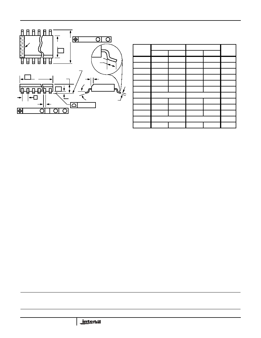
NOTES:
1. Symbols are defined in the "MO Series Symbol List" in Section
2.2 of Publication Number 95.
2. Dimensioning and tolerancing per ANSI Y14.5M-1982.
3. Dimension "D" does not include mold flash, protrusions or gate
burrs. Mold flash, protrusion and gate burrs shall not exceed
0.15mm (0.006 inch) per side.
4. Dimension "E" does not include interlead flash or protrusions.
Interlead flash and protrusions shall not exceed 0.25mm (0.010
inch) per side.
5. The chamfer on the body is optional. If it is not present, a visual
index feature must be located within the crosshatched area.
6. "L" is the length of terminal for soldering to a substrate.
7. "N" is the number of terminal positions.
8. Terminal numbers are shown for reference only.
9. The lead width "B", as measured 0.36mm (0.014 inch) or greater
above the seating plane, shall not exceed a maximum value of
0.61mm (0.024 inch)
10. Controlling dimension: MILLIMETER. Converted inch
dimensions are not necessarily exact.
INDEX
AREA
E
D
N
1
2
3
-B-
0.25(0.010)
C A
M
B S
e
-A-
L
B
M
-C-
A1
A
SEATING PLANE
0.10(0.004)
h x 45
o
C
H
µ
0.25(0.010)
B
M
M
M20.3
(JEDEC MS-013-AC ISSUE C)
20 LEAD WIDE BODY SMALL OUTLINE PLASTIC PACKAGE
SYMBOL
INCHES
MILLIMETERS
NOTES
MIN
MAX
MIN
MAX
A
0.0926
0.1043
2.35
2.65
-
A1
0.0040
0.0118
0.10
0.30
-
B
0.013
0.0200
0.33
0.51
9
C
0.0091
0.0125
0.23
0.32
-
D
0.4961
0.5118
12.60
13.00
3
E
0.2914
0.2992
7.40
7.60
4
e
0.050 BSC
1.27 BSC
-
H
0.394
0.419
10.00
10.65
-
h
0.010
0.029
0.25
0.75
5
L
0.016
0.050
0.40
1.27
6
N
20
20
7
0
o
8
o
0
o
8
o
-
Rev. 0 12/93
Small Outline Plastic Packages (SOIC)
HIP4080A