 | ÐлекÑÑоннÑй компоненÑ: HIP4082 | СкаÑаÑÑ:  PDF PDF  ZIP ZIP |
Äîêóìåíòàöèÿ è îïèñàíèÿ www.docs.chipfind.ru
1
CAUTION: These devices are sensitive to electrostatic discharge; follow proper IC Handling Procedures.
http://www.intersil.com or 407-727-9207
|
Copyright
©
Intersil Corporation 1999
HIP4082
80V, 1.25A Peak Current
H-Bridge FET Driver
Description
The HIP4082 is a medium frequency, medium voltage H-Bridge
N-Channel MOSFET driver IC, available in 16 lead plastic SOIC
(N) and DIP packages.
Specifically targeted for PWM motor control and UPS applica-
tions, bridge based designs are made simple and flexible with
the HIP4082 H-bridge driver. With operation up to 80V, the
device is best suited to applications of moderate power levels.
Similar to the HIP4081, it has a flexible input protocol for driving
every possible switch combination except those which would
cause a shoot-through condition. The HIP4082's reduced drive
current allows smaller packaging and it has a much wider range
of programmable dead times (0.1 to 4.5
µ
s) making it ideal for
switching frequencies up to 200kHz. The HIP4082 does not
contain an internal charge pump, but does incorporate non-
latching level-shift translation control of the upper drive circuits.
This set of features and specifications is optimized for applica-
tions where size and cost are important. For applications need-
ing higher drive capability the HIP4080A and HIP4081A are
recommended.
Ordering Information
PART
NUMBER
TEMPERATURE
RANGE
PACKAGE
HIP4082IB
-55
o
C to +125
o
C
16 Lead Plastic SOIC (N)
HIP4082IP
-55
o
C to +125
o
C
16 Lead Plastic DIP
Features
· Independently Drives 4 N-Channel FET in Half
Bridge or Full Bridge Configurations
· Bootstrap Supply Max Voltage to 95VDC
· Drives 1000pF Load in Free Air at 50
o
C with Rise
and Fall Times of Typically 15ns
· User-Programmable Dead Time (0.1 to 4.5
µ
s)
· DIS (Disable) Overrides Input Control and
Refreshes Bootstrap Capacitor when Pulled Low
· Input Logic Thresholds Compatible with 5V to 15V
Logic Levels
· Shoot-Through Protection
· Undervoltage Protection
Applications
· UPS Systems
· DC Motor Controls
· Full Bridge Power Supplies
· Class D Audio Power Amplifiers
· Noise Cancellation Systems
· Battery Powered Vehicles
· Peripherals
· Medium/Large Voice Coil Motors
March 1995
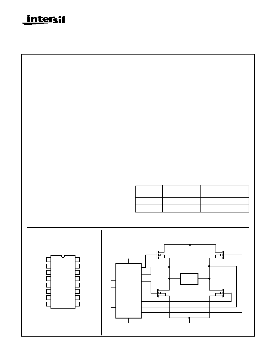
Pinout
HIP4082 (PDIP, SOIC)
TOP VIEW
14
15
16
9
13
12
11
10
1
2
3
4
5
7
6
8
BHB
BHI
BLI
ALI
DEL
V
SS
DIS
AHI
BHO
BLO
ALO
V
DD
AHS
AHO
AHB
BHS
Application Block Diagram
80V
GND
LOAD
HIP4082
GND
12V
AHI
ALI
BLI
BHI
BLO
BHS
BHO
ALO
AHS
AHO
File Number
3676.1
2
HIP4082
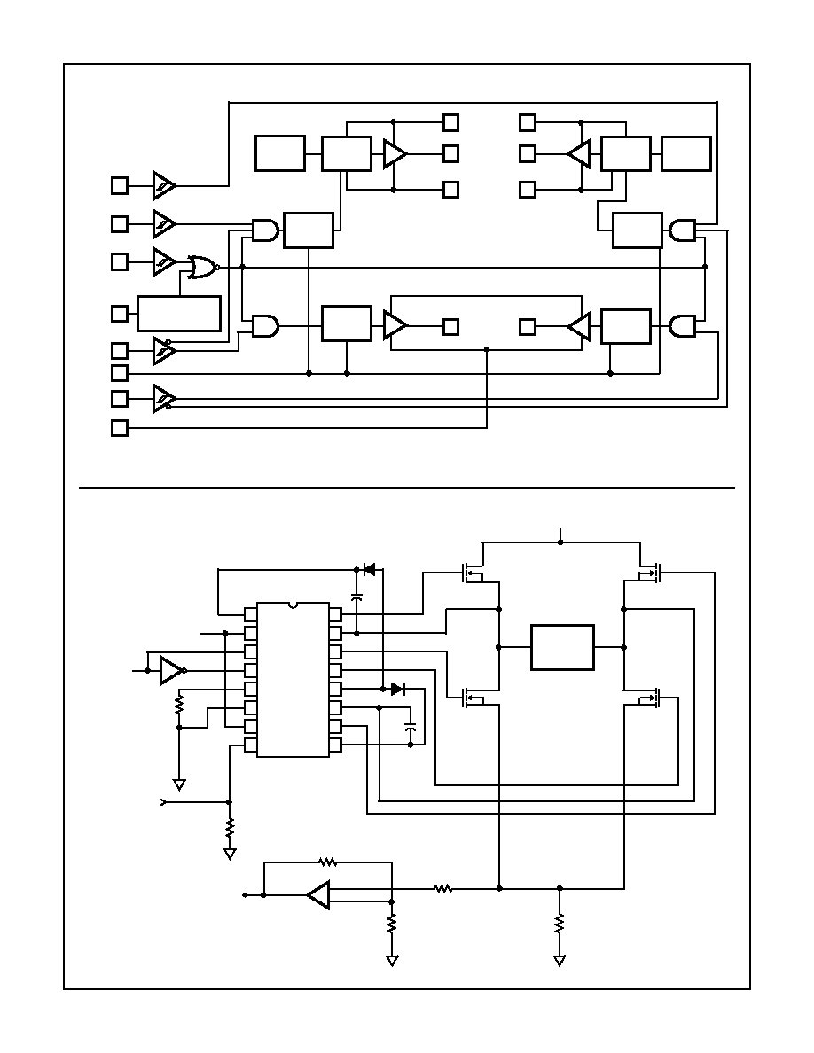
Functional Block Diagram
Typical Application (PWM Mode Switching)
3
8
2
7
4
12
5
6
TURN-ON
DELAY
DRIVER
13
LEVEL
SHIFT
DRIVER
AHB
AHS
9
10
11
14
15
16
1
DRIVER
TURN-ON
DELAY
DRIVER
TURN-ON
DELAY
LEVEL
SHIFT
AHO
BHB
BHS
BHO
ALO
BLO
TURN-ON
DELAY
UNDERVOLTAGE
DETECTOR
V
DD
BHI
AHI
DIS
ALI
V
DD
DEL
BLI
V
SS
U/V
U/V
80V
12V
12V
DIS
GND
GND
TO OPTIONAL
CURRENT CONTROLLER OR
PWM
LOAD
INPUT
+
-
14
15
16
9
13
12
11
10
1
2
3
4
5
7
6
8
BHB
BHI
BLI
ALI
DEL
V
SS
DIS
AHI
BHO
BLO
ALO
V
DD
AHS
AHO
AHB
BHS
OVERCURRENT LATCH
R
DIS
DELAY RESISTOR
FROM
OPTIONAL
OVERCURRENT
LATCH
R
SH
3
Specifications HIP4082
Absolute Maximum Ratings
Thermal Information
Supply Voltage, V
DD
. . . . . . . . . . . . . . . . . . . . . . . . . . . -0.3V to 16V
Logic I/O Voltages . . . . . . . . . . . . . . . . . . . . . . . -0.3V to V
DD
+0.3V
Voltage on AHS, BHS . . . . . .-6V (Transient) to 80V (25
o
C to 150
o
C)
Voltage on AHS, BHS . . . . . -6V (Transient) to 70V (-55
o
C to150
o
C)
Voltage on AHB, BHB . . . . . . . . . V
AHS, BHS
-0.3V to V
AHS, BHS
+V
DD
Voltage on ALO, BLO . . . . . . . . . . . . . . . . . .V
SS
-0.3V to V
DD
+0.3V
Voltage on AHO, BHO . . . V
AHS, BHS
-0.3V to V
AHB, BHB
+0.3V Input
Current, DEL . . . . . . . . . . . . . . . . . . . . . . . . . . . . . . . . -5mA to 0mA
Phase Slew Rate . . . . . . . . . . . . . . . . . . . . . . . . . . . . . . . . . . 20V/ns
NOTE: All voltages are relative V
SS
unless otherwise specified.
Thermal Resistance, Junction-Ambient
JA
SOIC Package . . . . . . . . . . . . . . . . . . . . . . . . . . . . .
115
o
C/W
DIP Package . . . . . . . . . . . . . . . . . . . . . . . . . . . . . .
90
o
C/W
Maximum Power Dissipation. . . . . . . . . . . . . . . . . . . . . . . . See Curve
Storage Temperature Range . . . . . . . . . . . . . . . . . . -65
o
C to +150
o
C
Operating Max. Junction Temperature . . . . . . . . . . . . . . . . . +150
o
C
Lead Temperature (Soldering 10s) . . . . . . . . . . . . . . . . . . . . +300
o
C
(For SOIC - Lead Tips Only))
CAUTION: Stresses above those listed in "Absolute Maximum Ratings" may cause permanent damage to the device. This is a stress only rating and operation
of the device at these or any other conditions above those indicated in the operational sections of this specification is not implied.
Operating Conditions
Supply Voltage, V
DD
. . . . . . . . . . . . . . . . . . . . . . . . . +8.5V to +15V
Voltage on V
SS
. . . . . . . . . . . . . . . . . . . . . . . . . . . . . . -1.0V to +1.0V
Voltage on AHB, BHB . . . . . . . . V
AHS, BHS
+7.5V to V
AHS, BHS
+V
DD
Input Current, DEL . . . . . . . . . . . . . . . . . . . . . . . . . -4mA to -100
µ
A
Electrical Specifications
V
DD
= V
AHB
= V
BHB
= 12V, V
SS
= V
AHS
= V
BHS
= 0V, R
DEL
= 100K
PARAMETER
SYMBOL
TEST CONDITIONS
T
J
= +25
o
C
T
J
= -55
o
C
TO +150
o
C
UNITS
MIN
TYP MAX
MIN
MAX
SUPPLY CURRENTS & UNDER VOLTAGE PROTECTION
V
DD
Quiescent Current
I
DD
All inputs = 0V, R
DEL
= 100K
1.2
2.3
3.5
0.85
4
mA
All inputs = 0V, R
DEL
= 10K
2.2
4.0
5.5
1.9
6.0
mA
V
DD
Operating Current
I
DDO
f = 50kHz, no load
1.5
2.6
4.0
1.1
4.2
mA
50kHz, no load, R
DEL
= 10k
2.5
4.0
6.4
2.1
6.6
mA
AHB, BHB Off Quiescent Current
I
AHBL
, I
BHBL
AHI = BHI = 0V
0.5
1.0
1.5
0.4
1.6
mA
AHB, BHB On Quiescent Current
I
AHBH
, I
BHBH
AHI = BHI = V
DD
65
145
240
40
250
µ
A
AHB, BHB Operating Current
I
AHBO
, I
BHBO
f = 50kHz, CL = 1000pF
.65
1.1
1.8
.45
2.0
mA
AHS, BHS Leakage Current
I
HLK
V
AHS
= V
BHS
= 80V
V
AHB
= V
BHB
= 96
-
-
1.0
-
-
µ
A
V
DD
Rising Undervoltage Threshold
V
DDUV+
6.8
7.6
8.25
6.5
8.5
V
V
DD
Falling Undervoltage Threshold
V
DDUV-
6.5
7.1
7.8
6.25
8.1
V
Undervoltage Hysteresis
UVHYS
0.17
0.4
0.75
0.15
0.90
V
AHB, BHB Undervoltage Threshold
VHBUV
Referenced to AHS & BHS
5
6.0
7
4.5
7.5
V
INPUT PINS: ALI, BLI, AHI, BHI, & DIS
Low Level Input Voltage
V
IL
Full Operating Conditions
-
-
1.0
-
0.8
V
High Level Input Voltage
V
IH
Full Operating Conditions
2.5
-
-
2.7
V
Input Voltage Hysteresis
-
35
-
-
-
mV
Low Level Input Current
I
IL
V
IN
= 0V, Full Operating Conditions
-145
-100
-60
-150
-50
µ
A
High Level Input Current
I
IH
V
IN
= 5V, Full Operating Conditions
-1
-
+1
-10
+10
µ
A
TURN-ON DELAY PIN DEL
Dead Time
T
DEAD
R
DEL
= 100K
2.5
4.5
8.0
2.0
8.5
µ
S
R
DEL
= 10K
0.27
0.5
0.75
0.2
0.85
µ
S
GATE DRIVER OUTPUT PINS: ALO, BLO, AHO, & BHO
Low Level Output Voltage
V
OL
I
OUT
= 50mA
0.65
1.1
0.5
1.2
V
High Level Output Voltage
V
DD
-V
OH
I
OUT
= -50mA
0.7
1.2
0.5
1.3
V
Peak Pullup Current
I
O
+
V
OUT
= 0V
1.1
1.4
2.5
0.85
2.75
A
Peak Pulldown Current
I
O
-
V
OUT
= 12V
1.0
1.3
2.3
0.75
2.5
A
4
Specifications HIP4082
Switching Specifications
V
DD
= V
AHB
= V
BHB
= 12V, V
SS
= V
AHS
= V
BHS
= 0V, R
DEL
= 100K, C
L
= 1000pF.
PARAMETER
SYMBOL
TEST CONDITIONS
T
J
= +25
o
C
T
J
= -55
o
C
TO +150
o
C
UNITS
MIN
TYP
MAX
MIN
MAX
Lower Turn-off Propagation Delay
(ALI-ALO, BLI-BLO)
T
LPHL
-
25
50
-
70
ns
Upper Turn-off Propagation Delay
(AHI-AHO, BHI-BHO)
T
HPHL
-
55
80
-
100
ns
Lower Turn-on Propagation Delay
(ALI-ALO, BLI-BLO)
T
LPLH
-
40
85
-
100
ns
Upper Turn-on Propagation Delay
(AHI-AHO, BHI-BHO)
T
HPLH
-
75
110
-
150
ns
Rise Time
T
R
-
9
20
-
25
ns
Fall Time
T
F
-
9
20
-
25
ns
Minimum Input Pulse Width
T
PWIN-ON/OFF
50
-
-
50
-
ns
Output Pulse Response to 50 ns Input Pulse
T
PWOUT
63
80
ns
Disable Turn-off Propagation Delay
(DIS - Lower Outputs)
T
DISLOW
-
50
80
-
90
ns
Disable Turn-off Propagation Delay
(DIS - Upper Outputs)
T
DISHIGH
-
75
100
-
125
ns
Disable Turn-on Propagation Delay
(DIS - ALO & BLO)
T
DLPLH
-
40
70
-
100
ns
Disable Turn-on Propagation Delay
(DIS- AHO & BHO)
T
DHPLH
R
DEL
= 10K
-
1.2
2
-
3
µ
s
Refresh Pulse Width (ALO & BLO)
T
REF-PW
375
580
900
350
950
ns
TRUTH TABLE
INPUT
OUTPUT
ALI, BLI
AHI, BHI
VDDUV
VHBUV
DIS
ALO, BLO
AHO, BHO
X
X
X
X
1
0
0
X
X
1
X
X
0
0
0
X
0
1
0
0
0
1
X
0
X
0
1
0
0
1
0
0
0
0
1
0
0
0
0
0
0
0
NOTE: X signifies that input can be either a "1" or "0".
5
HIP4082
Pin Descriptions
PIN
NUMBER
SYMBOL
DESCRIPTION
1
BHB
B High-side Bootstrap supply. External bootstrap diode and capacitor are required. Connect cathode of boot-
strap diode and positive side of bootstrap capacitor to this pin.
2
BHI
B High-side Input. Logic level input that controls BHO driver (Pin 16). BLI (Pin 3) high level input overrides BHI
high level input to prevent half-bridge shoot-through, see Truth Table. DIS (Pin 8) high level input overrides
BHI high level input. The pin can be driven by signal levels of 0V to 15V (no greater than V
DD
). An internal
100
µ
A pull-up to V
DD
will hold BHI high, so no connection is required if high-side and low-side outputs are to
be controlled by the low-side input.
3
BLI
B Low-side Input. Logic level input that controls BLO driver (Pin 14). If BHI (Pin 2) is driven high or not con-
nected externally then BLI controls both BLO and BHO drivers, with dead time set by delay currents at DEL
(Pin 5). DIS (Pin 8) high level input overrides BLI high level input. The pin can be driven by signal levels of 0V
to 15V (no greater than V
DD
). An internal 100
µ
A pull-up to V
DD
will hold BLI high if this pin is not driven.
4
ALI
A Low-side Input. Logic level input that controls ALO driver (Pin 13). If AHI (Pin 7) is driven high or not con-
nected externally then ALI controls both ALO and AHO drivers, with dead time set by delay currents at DEL
(Pin 5). DIS (Pin 8) high level input overrides ALI high level input. The pin can be driven by signal levels of 0V
to 15V (no greater than V
DD
). An internal 100
µ
A pull-up to V
DD
will hold ALI high if this pin is not driven.
5
DEL
Turn-on DELay. Connect resistor from this pin to V
SS
to set timing current that defines the dead time between
drivers. All drivers turn-off with no adjustable delay, so the DEL resistor guarantees no shoot-through by de-
laying the turn-on of all drivers. The voltage across the DEL resistor is approximately Vdd -2V.
6
V
SS
Chip negative supply, generally will be ground.
7
AHI
A High-side Input. Logic level input that controls AHO driver (Pin 10). ALI (Pin 4) high level input overrides AHI
high level input to prevent half-bridge shoot-through, see Truth Table. DIS (Pin 8) high level input overrides
AHI high level input. The pin can be driven by signal levels of 0V to 15V (no greater than V
DD
). An internal
100
µ
A pull-up to V
DD
will hold AHI high, so no connection is required if high-side and low-side outputs are to
be controlled by the low-side input.
8
DIS
DISable input. Logic level input that when taken high sets all four outputs low. DIS high overrides all other in-
puts. When DIS is taken low the outputs are controlled by the other inputs. The pin can be driven by signal
levels of 0V to 15V (no greater than V
DD
). An internal 100
µ
A pull-up to V
DD
will hold DIS high if this pin is not
driven.
9
AHB
A High-side Bootstrap supply. External bootstrap diode and capacitor are required. Connect cathode of boot-
strap diode and positive side of bootstrap capacitor to this pin.
10
AHO
A High-side Output. Connect to gate of A High-side power MOSFET.
11
AHS
A High-side Source connection. Connect to source of A High-side power MOSFET. Connect negative side of
bootstrap capacitor to this pin.
12
V
DD
Positive supply to control logic and lower gate drivers. De-couple this pin to V
SS
(Pin 6).
13
ALO
A Low-side Output. Connect to gate of A Low-side power MOSFET.
14
BLO
B Low-side Output. Connect to gate of B Low-side power MOSFET.
15
BHS
B High-side Source connection. Connect to source of B High-side power MOSFET. Connect negative side of
bootstrap capacitor to this pin.
16
BHO
B High-side Output. Connect to gate of B High-side power MOSFET.
6
HIP4082
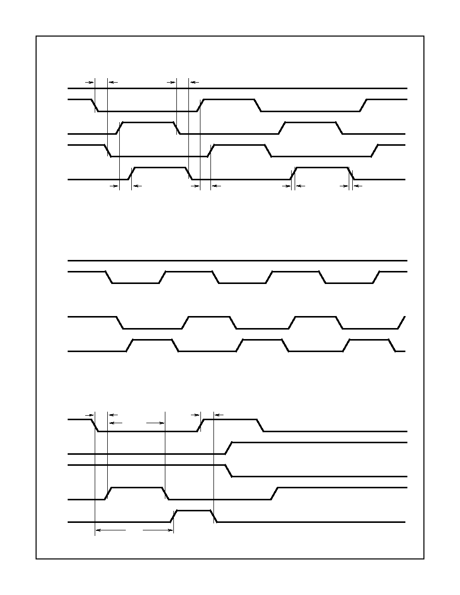
Timing Diagrams
FIGURE 1. INDEPENDENT MODE
FIGURE 2. BISTATE MODE
FIGURE 3. DISABLE FUNCTION
DIS=0
XLI
XHI
XLO
XHO
T
LPHL
T
HPHL
T
HPLH
T
LPLH
T
R
(10% - 90%)
T
F
(10% - 90%)
X = A OR B, A AND B HALVES OF BRIDGE CONTROLLER ARE INDEPENDENT
and UV
DIS=0
XLI
XHI = HI OR NOT CONNECTED
XLO
XHO
and UV
DIS or UV
XLI
XHI
XLO
XHO
T
DLPLH
T
DIS
T
DHPLH
T
REF-PW
7
HIP4082
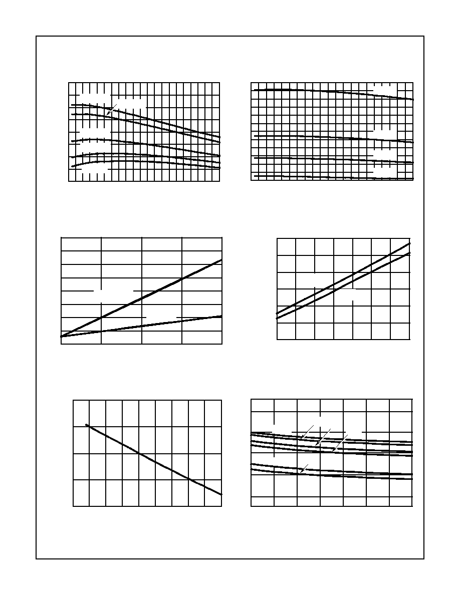
Performance Curves
FIGURE 4. I
DD
SUPPLY CURRENT vs TEMPERATURE AND
V
DD
SUPPLY VOLTAGE
FIGURE 5. V
DD
SUPPLY CURRENT vs TEMPERATURE AND
SWITCHING FREQUENCY (1000pF LOAD)
FIGURE 6. FLOATING (IXHB) BIAS CURRENT vs FREQUENCY
AND LOAD
FIGURE 7. GATE SOURCE/SINK PEAK CURRENT vs BIAS
SUPPLY VOLTAGE AT 25
o
C
FIGURE 8. GATE CURRENT vs TEMPERATURE, NORMALIZED
TO 25
o
C
FIGURE 9. V
DD
-V
OH
vs BIAS VOLTAGE TEMPERATURE
-60
-40
-20
0
20
40
60
80
100
120
140
1.5
1.75
2
2.25
2.5
2.75
3
3.25
3.5
JUNCTION TEMPERATURE (
o
C)
I
DD
SUPPL
Y CURRENT (mA)
V
DD
= 16V
V
DD
= 15V
V
DD
= 12V
V
DD
= 10V
V
DD
= 8V
-60
-40
-20
0
20
40
60
80
100
120
140
4
5
6
7
8
9
10
11
12
13
14
15
16
JUNCTION TEMPERATURE (
o
C)
I
DD
SUPPL
Y CURRENT (mA)
200kHz
100kHz
50kHz
10kHz
0
50
100
150
200
0
1
2
3
4
5
6
7
8
FREQUENCY (kHz)
LO
ADED
, NL BIAS CURRENTS (mA)
1000pF LOAD
NO LOAD
8
9
10
11
12
13
14
15
0.5
0.75
1
1.25
1.5
1.75
BIAS SUPPLY VOLTAGE (V) AT 25
o
C
PEAK GA
TE CURRENT (A)
1.925
0.815
I
SRC
(BIAS
)
I
SNK
(BIAS)
BIAS
2
8
15
SOURCE
SINK
-75
-50
-25
0
25
50
75
100
125
150
0.8
0.9
1
1.1
1.2
JUNCTION TEMPERATURE (
o
C)
NORMALIZED GA
TE
SINK/SOURCE CURRENT (A)
8
9
10
11
12
13
14
15
0.6
1
1.4
V
DD
SUPPLY VOLTAGE (V)
V
DD
-V
OH
(V)
1.2
0.8
-55
o
C
-40
o
C
0
o
C
25
o
C
125
o
C
150
o
C
8
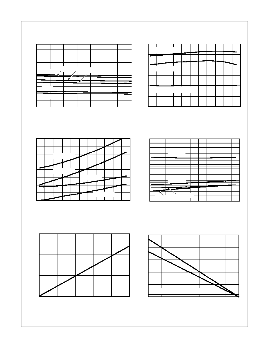
HIP4082
FIGURE 10. V
OL
vs BIAS VOLTAGE AND TEMPERATURE
FIGURE 11. UNDERVOLTAGE TRIP VOLTAGES vs TEMPERA-
TURE
FIGURE 12. UPPER LOWER TURN-ON
/
TURN-OFF PROPAGA-
TION DELAY vs TEMPERATURE
FIGURE 13. UPPER/LOWER DIS(ABLE) TO TURN-ON/OFF vs
TEMPERATURE (
o
C)
FIGURE 14. FULL BRIDGE LEVEL-SHIFT CURRENT vs
FREQUENCY (kHz)
FIGURE 15. MAXIMUM POWER DISSIPATION vs AMBIENT
TEMPERATURE
Performance Curves
(Continued)
8
9
10
11
12
13
14
1.4
V
DD
SUPPLY VOLTAGE (V)
V
OL
(V)
15
1.2
0.8
0.6
-55
o
C
-40
o
C
0
o
C
25
o
C
125
o
C
150
o
C
1
-60
-40
-20
0
20
40
60
80
100
120
140 160
5
5.5
6
6.5
7
7.5
8
JUNCTION TEMPERATURE (
o
C)
V
DD
, BIAS SUPPL
Y V
O
L
T
A
GE (V)
LOWER U/V RESET
LOWER U/V SET
UPPER U/V SET/RESET
-60
-40
-20
0
20
40
60
80
100
120
140 160
20
30
40
50
60
70
80
90
100
JUNCTION TEMPERATURE (
o
C)
PR
OP
A
G
A
TION DELA
YS (ns)
UPPER t
ON
UPPER t
OFF
LOWER t
ON
LOWER t
OFF
-60 -40
-20
0
20
40
60
80
100
120
140 160
10
100
10
4
JUNCTION TEMPERATURE (
o
C)
DIS T
O
TURN-ON
/OFF TIME (ns)
1000
DISHTON
DISHTOFF
DISLTON
DISLOFF
0
20
40
60
80
100
0.5
1
1.5
2
SWITCHING FREQUENCY (kHz)
LEVEL-SHIFT CURRENT (mA)
-60
-30
0
30
60
90
120
150
0
0.5
1
1.5
2
2.5
AMBIENT TEMPERATURE (
o
C)
T
O
T
AL PO
WER DISSIP
A
TION (W)
SOIC
16 PIN DIP
QUIESCENT BIAS COMPONENT

9
HIP4082
FIGURE 16. DEAD-TIME vs DEL RESISTANCE AND BIAS
SUPPLY (V
DD
) VOLTAGE
FIGURE 17. MAXIMUM OPERATING PEAK AHS/BHS VOLTAGE
vs TEMPERATURE
Performance Curves
(Continued)
0
10
20
30
40
50
60
70
80
90 100
100
1000
10
4
DEAD TIME RESISTANCE (k
)
DEAD TIME (ns)
V
DD
= 12V
V
DD
= 9V
V
DD
= 15V
100
50
0
50
100
150
70
75
80
85
90
TEMPERATURE (
o
C)
V
XHS
-V
SS
10
HIP4082
E16.3
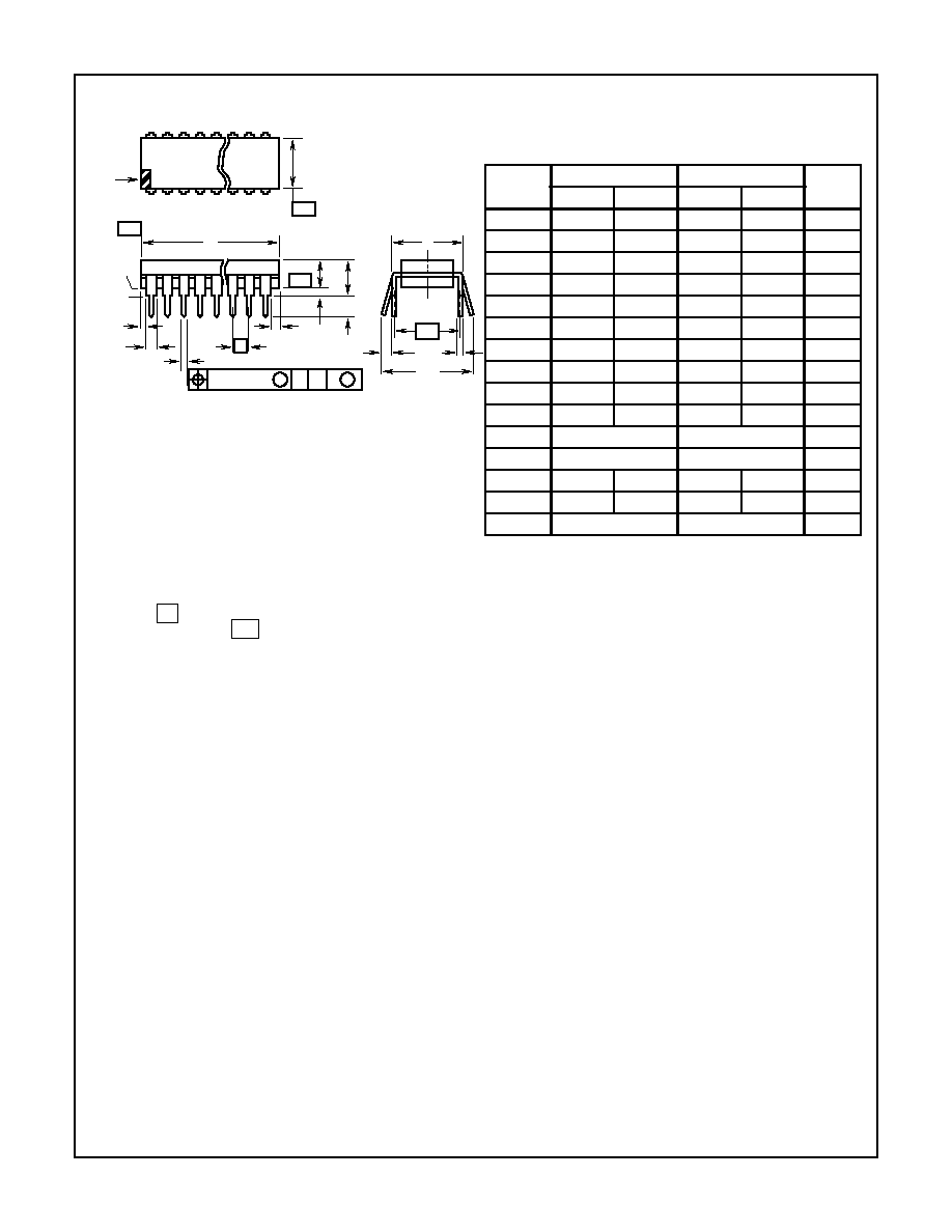
(JEDEC MS-001-BB ISSUE D)
16 LEAD DUAL-IN-LINE PLASTIC PACKAGE
SYMBOL
INCHES
MILLIMETERS
NOTES
MIN
MAX
MIN
MAX
A
-
0.210
-
5.33
4
A1
0.015
-
0.39
-
4
A2
0.115
0.195
2.93
4.95
-
B
0.014
0.022
0.356
0.558
-
B1
0.045
0.070
1.15
1.77
8, 10
C
0.008
0.014
0.204
0.355
-
D
0.735
0.775
18.66
19.68
5
D1
0.005
-
0.13
-
5
E
0.300
0.325
7.62
8.25
6
E1
0.240
0.280
6.10
7.11
5
e
0.100 BSC
2.54 BSC
-
e
A
0.300 BSC
7.62 BSC
6
e
B
-
0.430
-
10.92
7
L
0.115
0.150
2.93
3.81
4
N
16
16
9
Rev. 0 12/93
NOTES:
1. Controlling Dimensions: INCH. In case of conflict between
English and Metric dimensions, the inch dimensions control.
2. Dimensioning and tolerancing per ANSI Y14.5M-1982.
3. Symbols are defined in the "MO Series Symbol List" in Section
2.2 of Publication No. 95.
4. Dimensions A, A1 and L are measured with the package seated
in JEDEC seating plane gauge GS-3.
5. D, D1, and E1 dimensions do not include mold flash or protru-
sions. Mold flash or protrusions shall not exceed 0.010 inch
(0.25mm).
6. E and
are measured with the leads constrained to be per-
pendicular to datum
.
7. e
B
and e
C
are measured at the lead tips with the leads uncon-
strained. e
C
must be zero or greater.
8. B1 maximum dimensions do not include dambar protrusions.
Dambar protrusions shall not exceed 0.010 inch (0.25mm).
9. N is the maximum number of terminal positions.
10. Corner leads (1, N, N/2 and N/2 + 1) for E8.3, E16.3, E18.3,
E28.3, E42.6 will have a B1 dimension of 0.030 - 0.045 inch
(0.76 - 1.14mm).
C
L
E
e
A
C
e
B
e
C
-B-
E1
INDEX
1 2 3
N/2
N
AREA
SEATING
BASE
PLANE
PLANE
-C-
D1
B1
B
e
D
D1
A
A2
L
A1
-A-
0.010 (0.25)
C
A
M
B S
e
A
-C-
Dual-In-Line Plastic Packages (PDIP)
11
HIP4082
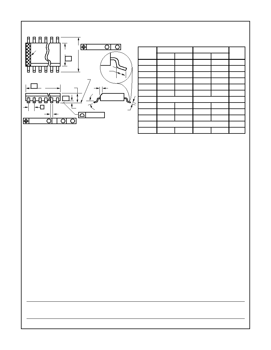
M16.15
(JEDEC MS-012-AC ISSUE C)
16 LEAD NARROW BODY SMALL OUTLINE PLASTIC PACKAGE
SYMBOL
INCHES
MILLIMETERS
NOTES
MIN
MAX
MIN
MAX
A
0.0532
0.0688
1.35
1.75
-
A1
0.0040
0.0098
0.10
0.25
-
B
0.013
0.020
0.33
0.51
9
C
0.0075
0.0098
0.19
0.25
-
D
0.3859
0.3937
9.80
10.00
3
E
0.1497
0.1574
3.80
4.00
4
e
0.050 BSC
1.27 BSC
-
H
0.2284
0.2440
5.80
6.20
-
h
0.0099
0.0196
0.25
0.50
5
L
0.016
0.050
0.40
1.27
6
N
16
16
7
0
o
8
o
0
o
8
o
-
Rev. 0 12/93
NOTES:
1. Symbols are defined in the "MO Series Symbol List" in Section
2.2 of Publication Number 95.
2. Dimensioning and tolerancing per ANSI Y14.5M-1982.
3. Dimension "D" does not include mold flash, protrusions or gate
burrs. Mold flash, protrusion and gate burrs shall not exceed
0.15mm (0.006 inch) per side.
4. Dimension "E" does not include interlead flash or protrusions. In-
terlead flash and protrusions shall not exceed 0.25mm (0.010
inch) per side.
5. The chamfer on the body is optional. If it is not present, a visual
index feature must be located within the crosshatched area.
6. "L" is the length of terminal for soldering to a substrate.
7. "N" is the number of terminal positions.
8. Terminal numbers are shown for reference only.
9. The lead width "B", as measured 0.36mm (0.014 inch) or greater
above the seating plane, shall not exceed a maximum value of
0.61mm (0.024 inch)
10. Controlling dimension: MILLIMETER. Converted inch dimen-
sions are not necessarily exact.
INDEX
AREA
E
D
N
1
2
3
-B-
0.25(0.010)
C A
M
B S
e
-A-
L
B
M
-C-
A1
A
SEATING PLANE
0.10(0.004)
h x 45
o
C
H
0.25(0.010)
B
M
M
Small Outline Plastic Packages (SOIC)
All Intersil semiconductor products are manufactured, assembled and tested under ISO9000 quality systems certification.
Intersil products are sold by description only. Intersil Corporation reserves the right to make changes in circuit design and/or specifications at any time without
notice. Accordingly, the reader is cautioned to verify that data sheets are current before placing orders. Information furnished by Intersil is believed to be accurate
and reliable. However, no responsibility is assumed by Intersil or its subsidiaries for its use; nor for any infringements of patents or other rights of third parties which
may result from its use. No license is granted by implication or otherwise under any patent or patent rights of Intersil or its subsidiaries.
For information regarding Intersil Corporation and its products, see web site http://www.intersil.com