1
Æ
80V, 1.25A Peak Current H-Bridge FET
Driver
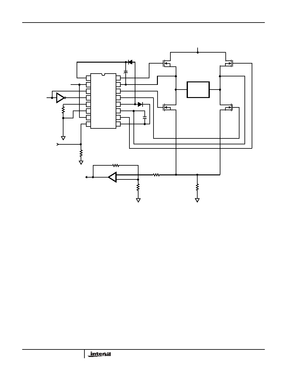
The HIP4082 is a medium frequency, medium voltage
H-Bridge N-Channel MOSFET driver IC, available in 16 lead
plastic SOIC (N) and DIP packages.
Specifically targeted for PWM motor control and UPS
applications, bridge based designs are made simple and
flexible with the HIP4082 H-bridge driver. With operation up
to 80V, the device is best suited to applications of moderate
power levels.
Similar to the HIP4081, it has a flexible input protocol for
driving every possible switch combination except those
which would cause a shoot-through condition. The
HIP4082's reduced drive current allows smaller packaging
and it has a much wider range of programmable dead times
(0.1 to 4.5
µ
s) making it ideal for switching frequencies up to
200kHz. The HIP4082 does not contain an internal charge
pump, but does incorporate non-latching level-shift
translation control of the upper drive circuits.
This set of features and specifications is optimized for
applications where size and cost are important. For
applications needing higher drive capability the HIP4080A
and HIP4081A are recommended.
Pinout
Features
∑ Independently Drives 4 N-Channel FET in Half Bridge or
Full Bridge Configurations
∑ Bootstrap Supply Max Voltage to 95VDC
∑ Drives 1000pF Load in Free Air at 50
o
C with Rise and Fall
Times of Typically 15ns
∑ User-Programmable Dead Time (0.1 to 4.5
µ
s)
∑ DIS (Disable) Overrides Input Control and Refreshes
Bootstrap Capacitor when Pulled Low
∑ Input Logic Thresholds Compatible with 5V to 15V Logic
Levels
∑ Shoot-Through Protection
∑ Undervoltage Protection
Applications
∑ UPS Systems
∑ DC Motor Controls
∑ Full Bridge Power Supplies
∑ Switching Power Amplifiers
∑ Noise Cancellation Systems
∑ Battery Powered Vehicles
∑ Peripherals
∑ Medium/Large Voice Coil Motors
∑ Related Literature
- TB363, Guidelines for Handling and Processing
Moisture Sensitive Surface Mount Devices (SMDs)
Ordering Information
PART
NUMBER
TEMPERATURE
RANGE
PACKAGE
HIP4082IB
-55
o
C to +125
o
C
16 Lead Plastic SOIC (N)
HIP4082IP
-55
o
C to +125
o
C
16 Lead Plastic DIP
14
15
16
9
13
12
11
10
1
2
3
4
5
7
6
8
BHB
BHI
BLI
ALI
DEL
V
SS
DIS
AHI
BHO
BLO
ALO
V
DD
AHS
AHO
AHB
BHS
HIP4082
(PDIP, SOIC)
TOP VIEW
February 2003
HIP4082
Data Sheet
FN3676.2
CAUTION: These devices are sensitive to electrostatic discharge; follow proper IC Handling Procedures.
1-888-INTERSIL or 321-724-7143
|
Intersil (and design) is a registered trademark of Intersil Americas Inc.
Copyright © Intersil Americas Inc. 2003. All Rights Reserved
All other trademarks mentioned are the property of their respective owners.
4
Absolute Maximum Ratings
Thermal Information
Supply Voltage, V
DD
. . . . . . . . . . . . . . . . . . . . . . . . . . . .-0.3V to 16V
Logic I/O Voltages . . . . . . . . . . . . . . . . . . . . . . . -0.3V to V
DD
+0.3V
Voltage on AHS, BHS. . . . . . -6V (Transient) to 80V (25
o
C to 150
o
C)
Voltage on AHS, BHS. .. . . . -6V (Transient) to 70V (-55
o
C to150
o
C)
Voltage on AHB, BHB. . . . . . . . . V
AHS, BHS
-0.3V to V
AHS, BHS
+V
DD
Voltage on ALO, BLO . . . . . . . . . . . . . . . . . .V
SS
-0.3V to V
DD
+0.3V
Voltage on AHO, BHO . . . V
AHS, BHS
-0.3V to V
AHB, BHB
+0.3V Input
Current, DEL . . . . . . . . . . . . . . . . . . . . . . . . . . . . . . . . -5mA to 0mA
Phase Slew Rate . . . . . . . . . . . . . . . . . . . . . . . . . . . . . . . . . . 20V/ns
NOTE:
All voltages are relative V
SS
unless otherwise specified.
Thermal Resistance, Junction-Ambient . . . . . . . . . . . . . . . . . . . .
JA
SOIC Package. . . . . . . . . . . . . . . . . . . . . . . . . . . . . . . . . 115
o
C/W
DIP Package . . . . . . . . . . . . . . . . . . . . . . . . . . . . . . . . . . . 90
o
C/W
Maximum Power Dissipation. . . . . . . . . . . . . . . . . . . . . . . . See Curve
Storage Temperature Range. . . . . . . . . . . . . . . . . . -65
o
C to +150
o
C
Operating Max. Junction Temperature . . . . . . . . . . . . . . . . . +150
o
C
Lead Temperature (Soldering 10s) . . . . . . . . . . . . . . . . . . . . +300
o
C
(For SOIC - Lead Tips Only))
Operating Conditions
Supply Voltage, V
DD
. . . . . . . . . . . . . . . . . . . . . . . . . +8.5V to +15V
Voltage on V
SS
. . . . . . . . . . . . . . . . . . . . . . . . . . . . . . -1.0V to +1.0V
Voltage on AHB, BHB. . . . . . . . .V
AHS, BHS
+7.5V to V
AHS, BHS
+V
DD
Input Current, DEL . . . . . . . . . . . . . . . . . . . . . . . . . -4mA to -100
µ
A
CAUTION: Stresses above those listed in "Absolute Maximum Ratings" may cause permanent damage to the device. This is a stress only rating and operation of the
device at these or any other conditions above those indicated in the operational sections of this specification is not implied.
Electrical Specifications
V
DD
= V
AHB
= V
BHB
= 12V, V
SS
= V
AHS
= V
BHS
= 0V, R
DEL
= 100K
PARAMETER
SYMBOL
TEST CONDITIONS
T
J
= +25
o
C
T
J
= -55
o
C
TO +150
o
C
UNITS
MIN
TYP
MAX
MIN
MAX
SUPPLY CURRENTS & UNDER VOLTAGE PROTECTION
V
DD
Quiescent Current
I
DD
All inputs = 0V, R
DEL
= 100K
1.2
2.3
3.5
0.85
4
mA
All inputs = 0V, R
DEL
= 10K
2.2
4.0
5.5
1.9
6.0
mA
V
DD
Operating Current
I
DDO
f = 50kHz, no load
1.5
2.6
4.0
1.1
4.2
mA
50kHz, no load, R
DEL
= 10k
2.5
4.0
6.4
2.1
6.6
mA
AHB, BHB Off Quiescent Current
I
AHBL
, I
BHBL
AHI = BHI = 0V
0.5
1.0
1.5
0.4
1.6
mA
AHB, BHB On Quiescent Current
I
AHBH
, I
BHBH
AHI = BHI = V
DD
65
145
240
40
250
µ
A
AHB, BHB Operating Current
I
AHBO
, I
BHBO
f = 50kHz, CL = 1000pF
.65
1.1
1.8
.45
2.0
mA
AHS, BHS Leakage Current
I
HLK
V
AHS
= V
BHS
= 80V
V
AHB
= V
BHB
= 96
-
-
1.0
-
-
µ
A
V
DD
Rising Undervoltage Threshold
V
DDUV+
6.8
7.6
8.25
6.5
8.5
V
V
DD
Falling Undervoltage Threshold
V
DDUV-
6.5
7.1
7.8
6.25
8.1
V
Undervoltage Hysteresis
UVHYS
0.17
0.4
0.75
0.15
0.90
V
AHB, BHB Undervoltage Threshold
VHBUV
Referenced to AHS & BHS
5
6.0
7
4.5
7.5
V
INPUT PINS: ALI, BLI, AHI, BHI, & DIS
Low Level Input Voltage
V
IL
Full Operating Conditions
-
-
1.0
-
0.8
V
High Level Input Voltage
V
IH
Full Operating Conditions
2.5
-
-
2.7
V
Input Voltage Hysteresis
-
35
-
-
-
mV
Low Level Input Current
I
IL
V
IN
= 0V, Full Operating Conditions
-145
-100
-60
-150
-50
µ
A
High Level Input Current
I
IH
V
IN
= 5V, Full Operating Conditions
-1
-
+1
-10
+10
µ
A
TURN-ON DELAY PIN DEL
Dead Time
T
DEAD
R
DEL
= 100K
2.5
4.5
8.0
2.0
8.5
µ
S
R
DEL
= 10K
0.27
0.5
0.75
0.2
0.85
µ
S
GATE DRIVER OUTPUT PINS: ALO, BLO, AHO, & BHO
Low Level Output Voltage
V
OL
I
OUT
= 50mA
0.65
1.1
0.5
1.2
V
High Level Output Voltage
V
DD
-V
OH
I
OUT
= -50mA
0.7
1.2
0.5
1.3
V
HIP4082
5
Peak Pullup Current
I
O
+
V
OUT
= 0V
1.1
1.4
2.5
0.85
2.75
A
Peak Pulldown Current
I
O
-
V
OUT
= 12V
1.0
1.3
2.3
0.75
2.5
A
Switching Specifications
V
DD
= V
AHB
= V
BHB
= 12V, V
SS
= V
AHS
= V
BHS
= 0V, R
DEL
= 100K, C
L
= 1000pF.
PARAMETER
SYMBOL
TEST CONDITIONS
T
J
= +25
o
C
T
J
= -55
o
C TO
+150
o
C
UNITS
MIN
TYP
MAX
MIN
MAX
Lower Turn-off Propagation Delay
(ALI-ALO, BLI-BLO)
T
LPHL
-
25
50
-
70
ns
Upper Turn-off Propagation Delay
(AHI-AHO, BHI-BHO)
T
HPHL
-
55
80
-
100
ns
Lower Turn-on Propagation Delay
(ALI-ALO, BLI-BLO)
T
LPLH
-
40
85
-
100
ns
Upper Turn-on Propagation Delay
(AHI-AHO, BHI-BHO)
T
HPLH
-
75
110
-
150
ns
Rise Time
T
R
-
9
20
-
25
ns
Fall Time
T
F
-
9
20
-
25
ns
Minimum Input Pulse Width
T
PWIN-ON/OFF
50
-
-
50
-
ns
Output Pulse Response to 50 ns Input Pulse
T
PWOUT
63
80
ns
Disable Turn-off Propagation Delay
(DIS - Lower Outputs)
T
DISLOW
-
50
80
-
90
ns
Disable Turn-off Propagation Delay
(DIS - Upper Outputs)
T
DISHIGH
-
75
100
-
125
ns
Disable Turn-on Propagation Delay
(DIS - ALO & BLO)
T
DLPLH
-
40
70
-
100
ns
Disable Turn-on Propagation Delay
(DIS- AHO & BHO)
T
DHPLH
R
DEL
= 10K
-
1.2
2
-
3
µ
s
Refresh Pulse Width (ALO & BLO)
T
REF-PW
375
580
900
350
950
ns
TRUTH TABLE
INPUT
OUTPUT
ALI, BLI
AHI, BHI
VDDUV
VHBUV
DIS
ALO, BLO
AHO, BHO
X
X
X
X
1
0
0
X
X
1
X
X
0
0
0
X
0
1
0
0
0
1
X
0
X
0
1
0
0
1
0
0
0
0
1
0
0
0
0
0
0
0
NOTE:
X signifies that input can be either a "1" or "0".
Electrical Specifications
V
DD
= V
AHB
= V
BHB
= 12V, V
SS
= V
AHS
= V
BHS
= 0V, R
DEL
= 100K (Continued)
PARAMETER
SYMBOL
TEST CONDITIONS
T
J
= +25
o
C
T
J
= -55
o
C
TO +150
o
C
UNITS
MIN
TYP
MAX
MIN
MAX
HIP4082