Document Outline
- 1.� qJA is measured with the component mounted on an evaluation PC board in free air.
- 2.� All voltages are relative to VSS unless otherwise specified.
- 3.� x = A, B, C, and D. For example, xHS refers to AHS, BHS, CHS, and DHS.
- 3
- 4
- 5
- 2
- 6
- mA
- 8
- 9.5
- 12
- 7
- 13
- mA
- -
- 40
- 80
- -
- 100
- mA
- 0.6
- 0.8
- 1.3
- 0.5
- 1.4
- mA
- 0.7
- 0.9
- 1.3
- 2.0
- mA
- 11.5
- 12.5
- 14
- 10.5
- 14.5
- V
- -
- 100
- 130
- -
- 140
- mA
- 7
- 24
- 45
- -
- 50
- mA
- 6.2
- 7.1
- 8.0
- 6.1
- 8.1
- V
- 5.75
- 6.6
- 7.5
- 5.6
- 7.6
- V
- 5
- 6.2
- 6.8
- 4.9
- 6.9
- V
- -
- -
- 1.0
- -
- 0.8
- V
- 2.5
- -
- -
- 2.7
- -
- V
- -
- 35
- -
- -
- -
- mV
- 60
- 100
- 135
- 55
- 140
- mA
- -1
- -
- 1
- -10
- 10
- mA
- -
- 100
- -
- -
- 200
- mV
- 0.3
- 0.5
- 0.7
- -
- 1.0
- A
- 0.7
- 1.1
- 1.5
- 0.5
- 1.7
- A
- 3.8
- 4.5
- 6
- 3
- 7
- ms
- 0.38
- 0.5
- 0.65
- 0.3
- 0.7
- ms
- -
- 7
- 15
- -
- 20
- %
- -
- 25
- 50
- -
- 70
- ns
- -
- 55
- 80
- -
- 100
- ns
- -
- 40
- 85
- -
- 100
- ns
- -
- 75
- 110
- -
- 150
- ns
- -
- 20
- 40
- -
- 50
- ns
- -
- 10
- 20
- -
- 25
- ns
- 50
- -
- -
- 50
- -
- ns
- 50
- -
- -
- 50
- -
- ns
- -
- 50
- 80
- 90
- ns
- -
- 75
- 100
- -
- 125
- ns
- -
- 50
- 80
- -
- 100
- ns
- -
- 1.2
- 2
- -
- 3
- ms
- 375
- 580
- 900
- 350
- 950
- ms
- A
- -
- A1
- -
- B
- 9
- C
- -
- D
- 3
- E
- 4
- e
- 0.05 BSC
- 1.27 BSC
- -
- H
- -
- h
- 5
- L
- 6
- N
- 28
- 28
- 7
- a
- 0o
- 8o
- 0o
- 8o
- -
- 1.� Controlling Dimensions: INCH. In case of conflict between En�glish and Metric dimensions, the...
- 2.� Dimensioning and tolerancing per ANSI Y14.5M-1982.
- 3.� Symbols are defined in the �MO Series Symbol List� in Section 2.2 of Publication No. 95.
- 4.� Dimensions A, A1 and L are measured with the package seated in JEDEC seating plane gauge GS-3.
- 5.� D, D1, and E1 dimensions do not include mold flash or protrusions. Mold flash or protrusions ...
- 6.� E and��are measured with the leads constrained to be perpendicular to datum .
- 7.� eB and eC are measured at the lead tips with the leads unconstrained. eC must be zero or grea...
- 8.� B1 maximum dimensions do not include dambar protrusions. Dambar protrusions shall not exceed ...
- 9.� N is the maximum number of terminal positions.
- 10.� Corner leads (1, N, N/2 and N/2 + 1) for E8.3, E16.3, E18.3, E28.3, E42.6 will have a B1 dim...
- A
- -
- -
- 4
- A1
- -
- -
- 4
- A2
- -
- B
- -
- B1
- 8
- C
- -
- D
- 5
- D1
- -
- -
- 5
- E
- 6
- E1
- 5
- e
- 0.100 BSC
- 2.54 BSC
- -
- eA
- 0.600 BSC
- 15.24 BSC
- 6
- eB
- -
- -
- 7
- L
- 4
- N
- 28
- 28
- 9
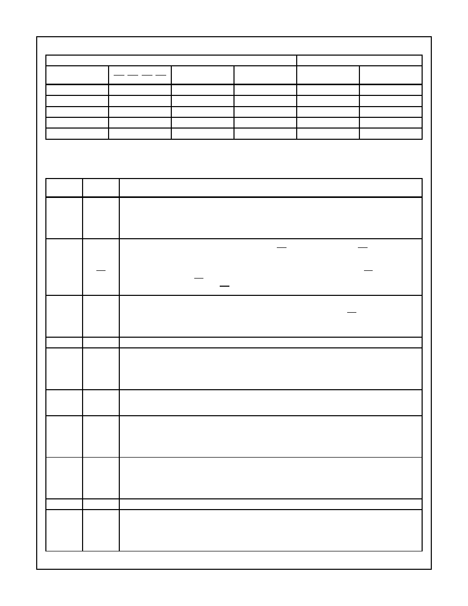
- TRUTH TABLE
- February 1998
- HIP4084
1
�
PRELIMINARY
February 1998
HIP4084
80V, 0.50A Four Phase Driver
Features
� Independently Drives 8 N-Channel MOSFETs in Either
Four Phase Bridge Configuration or Dual H-Bridge
Configuration
� 1.25A Peak Turn-Off Current
� Bootstrap Supply Max Voltage to 95VDC
� Bias Supply Operation from 7V to 15V
� User-Programmable Dead Time (0.25
�s to 4.5�s)
� Charge-Pump and Bootstrap Maintain Upper Bias
Supplies
� Drives 1000pF Load with Typical Rise Time of 20ns
and Fall Time of 10ns
� EN (Disable) Overrides Input Control
� Input Logic Thresholds Compatible with 3V to 15V
Logic Levels
� Dead Time Disable Capability
� Programmable Undervoltage Set Point
Applications
� Brushless Motors
� AC Motor Drives
� Stepper Motors
� Switched Reluctance Motor Drives
Description
The HIP4084 is a Four Phase Bridge N-Channel MOSFET
driver IC.
Specifically targeted for PWM and stepper motor control
applications, the HIP4084 makes bridge based designs sim-
ple and flexible. With operation up to 80V and undervoltage
detection, the device is best suited to applications of moder-
ate power levels.
Like the HIP4081, the HIP4084 has a flexible input protocol
for driving every possible switch combination. Like the
HIP4082, the HIP4084 provides a typical drive currents of
0.5A and a programmable dead time from 0.25
�s to 4.5�s.
Like the HIP4086, the HIP4084 allows override of shoot-
through protection for switched reluctance applications. The
HIP4084 is suitable for applications requiring DC to 100kHz.
Unlike other HIP4080 family products, the HIP4084 pro-
vides, from a single pin, a programmable undervoltage set
point and an enable/disable function.
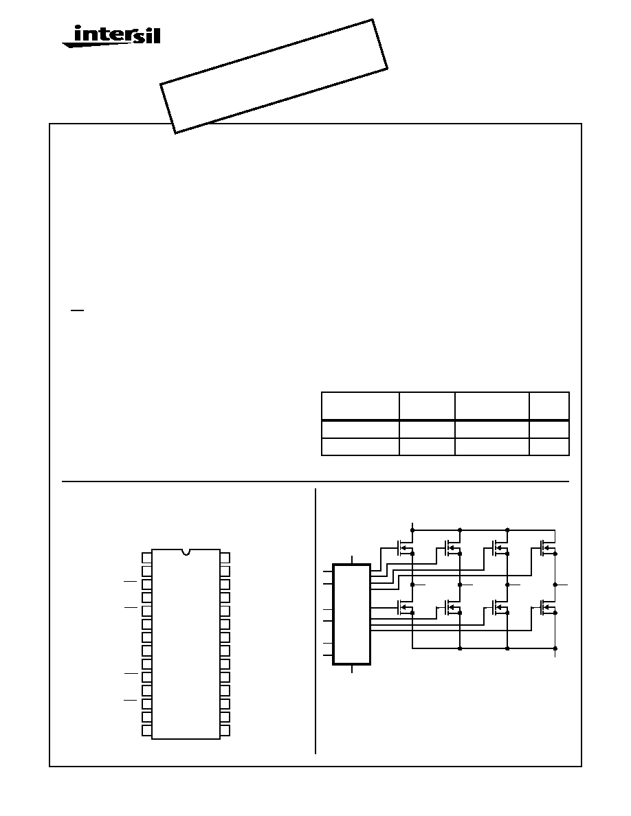
Pinout
HIP4084
(PDIP, SOIC)
TOP VIEW
Application Block Diagram
Ordering Information
PART NUMBER
TEMP.
RANGE (
o
C)
PACKAGE
PKG.
NO.
HIP4084AB
-40 to 105
28 Ld SOIC
M28.3
HIP4084AP
-40 to 105
28 Ld PDIP
E28.6
For additional information contact Ivars Lauzums at (407) 729-5531.
28
27
26
25
24
23
22
21
20
19
18
17
16
15
1
2
3
4
5
6
7
8
9
10
11
12
13
14
AHB
AHI
ALI
CLO
AHO
V
DD
BLI
CHI
CLI
UVLO/EN
CHB
BLO
CHO
CHS
BHB
BHI
BHO
BHS
DHI
DLI
DLO
DHB
DHO
DHS
ALO
R
DEL
AHS
V
SS
HIP4084
12V
80V
GND
GND
CAUTION: These devices are sensitive to electrostatic discharge; follow proper IC Handling Procedures.
1-888-INTERSIL or 321-724-7143
|
Intersil (and design) is a registered trademark of Intersil Americas Inc.
Copyright � Intersil Americas Inc. 2002. All Rights Reserved
File Number
4222.1
NOT
REC
OMM
END
ED F
OR N
EW D
ESIG
NS
See
HIP4
082
or co
ntac
t our
Tec
hnic
al Su
ppor
t Cen
ter a
t
1-88
8-INT
ERS
IL or
www
.inte
rsil.c
om/t
sc
2
TRUTH TABLE
INPUT
OUTPUT
ALI, BLI, CLI, DLI
AHI, BHI, CHI, DHI
UVLO/EN
R
DEL
ALO, BLO,
CLO, DLO
AHO, BHO,
CHO, DHO
X
X
0
X
0
0
1
X
1
>100mV
1
0
0
0
1
X
0
1
0
1
1
X
0
0
1
0
1
<100mV
1
1
NOTE: X signifies that input can be either a "1" or "0".
Pin Descriptions
PIN
NUMBER
SYMBOL
DESCRIPTION
2
27
17
14
AHB
BHB
CHB
DHB
(xHB)
High-side Bootstrap supplies. One external bootstrap diode and one capacitor are required for each. Connect
cathode of bootstrap diode and positive side of bootstrap capacitor to each xHB pin.
3
5
10
12
AHI
BHI
CHI
DHI
(xHI)
High-Side Logic Level Inputs. Logic at these three pins controls the three high-side output drivers, AHO (Pin 1),
BHO (Pin 26) and CHO (Pin 18) and DHO (Pin 15). When xHI is low, xHO is high. When xHI is high, xHO is low.
Unless the dead time is disabled by connecting R
DEL
(Pin 8) to ground, the low side input of each phase will
override the corresponding high side input on that phase. If R
DEL
is tied to ground, dead time is disabled and
the outputs follow the inputs. Care must be taken to avoid shoot-through in this application. EN (Pin 9) also over-
rides the high side inputs. xHI can be driven by signal levels of 0V to 15V (no greater than V
DD
). An internal
100
�A pull-up to V
DD
will hold each xHI high if the pins are not driven.
4
6
11
13
ALI
BLI
CLI
DLI
(xLI)
Low-Side Logic Level Inputs. Logic at these three pins controls the three low-side output drivers ALO (Pin 24),
BLO (Pin 23) and CLO (Pin 21) and DLO (Pin 20). If the upper inputs are grounded then the lower inputs controls
both xLO and xHO drivers, with the dead time set by the resistor at R
DEL
(Pin 8). EN (Pin 9) high level input
overrides xLI, forcing all outputs low. xLI can be driven by signal levels of 0V to 15V (no greater than V
DD
). An
internal 100
�A pull-up to V
DD
will hold xLI high if these pins are not driven.
7
V
SS
Ground. Connect the sources of the low-side power MOSFETs to this pin.
8
R
DEL
Dead Time Setting. Connect resistor from this pin to V
DD
to set timing current that defines the dead time be-
tween drivers. All drivers turn-off with no adjustable delay, so the R
DEL
resistor guarantees no shoot-through by
delaying the turn-on of all drivers. When R
DEL
is tied to V
SS
, both upper and lowers can be commanded on
simultaneously. While not necessary in most applications, a decoupling capacitor of 0.1
�F or smaller may be
connected between R
DEL
and V
SS
.
9
RUV/EN
A resistor can be connected between this pin and V
SS
to program the under voltage set point. With this pin not
connected the undervoltage setpoint is typically 6.6V. When this pin is tied to V
DD
, the undervoltage setpoint is
typically 6.2V. With this pin tied to V
SS
, all six outputs are taken low, overriding all other inputs.
1
26
18
15
AHO
BHO
CHO
DHO
(xHO)
High-Side Outputs. Connect the gates of the high-side power MOSFETs to these pins.
28
25
19
16
AHS
BHS
CHS
DHS
(xHS)
High-Side Source connection. Connect the sources of the high-side power MOSFETs to these pins. The nega-
tive side of the bootstrap capacitors should also be connected to these pins.
22
V
DD
Positive supply. De-couple this pin to V
SS
(Pin 7).
24
23
21
20
ALO
BLO
CLO
DLO
(xLO)
Low-Side Outputs. Connect the gates of the low-side power MOSFETs to these pins.
NOTE: x = A, B, C and D
HIP4084
3
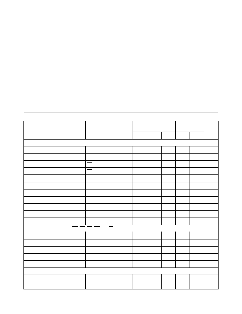
Absolute Maximum Ratings
T
A
= 25
o
C
Thermal Information
Supply Voltage, V
DD
. . . . . . . . . . . . . . . . . . . . . . . . . . -0.3V to 16V
Logic I/O Voltages . . . . . . . . . . . . . . . . . . . . . . . -0.3V to V
DD
+0.3V
Voltage on xHS. . . . . . . . .-6V (Transient) to +85V (-40
o
C to 150
o
C)
Voltage on xHB. . . . . . . . . . . . . . . . . . . . .V
xHS
-0.3V to V
xHS
+V
DD
Voltage on xLO. . . . . . . . . . . . . . . . . . . . . . V
SS
-0.3V to V
DD
+0.3V
Voltage on xHO . . . . . . . . . . . . . . . . . . . .V
xHS
-0.3V to V
xHB
+0.3V
Phase Slew Rate . . . . . . . . . . . . . . . . . . . . . . . . . . . . . . . . . . 20V/ns
Operating Conditions
Supply Voltage, V
DD
. . . . . . . . . . . . . . . . . . . . . . . . . +7.0V to +15V
Voltage on V
xHS
. . . . . . . . . . . . . . . . . . . . . . . . . . . . . . . . .0V to 80V
Voltage on xHB. . . . . . . . . . . . . . . . . . . . . . . . . . . . . . . .V
xHS
+ V
DD
Thermal Resistance (Typical, Note 1)
JA
(
o
C/W)
SOIC Package. . . . . . . . . . . . . . . . . . . . . . . . . . . . .
75
o
C
PDIP Package . . . . . . . . . . . . . . . . . . . . . . . . . . . . .
65
o
C
Maximum Junction Temperature. . . . . . . . . . . . . . . . . . . . . . . 150
o
C
Maximum Storage Temperature Range . . . . . . . . . . -65
o
C to 150
o
C
Maximum Lead Temperature (Soldering 10s). . . . . . . . . . . . . 300
o
C
(SOIC - Lead Tips Only)
Operating Ambient Temperature Range . . . . . . . . . . -40
o
C to 105
o
C
Operating Junction Temperature Range . . . . . . . . .-40
o
C to 105
o
C
CAUTION: Stresses above those listed in "Absolute Maximum Ratings" may cause permanent damage to the device. This is a stress only rating and operation
of the device at these or any other conditions above those indicated in the operational sections of this specification is not implied.
NOTES:
1.
JA
is measured with the component mounted on an evaluation PC board in free air.
2. All voltages are relative to VSS unless otherwise specified.
3. x = A, B, C, and D. For example, xHS refers to AHS, BHS, CHS, and DHS.
Electrical Specifications
V
DD
= V
xHB
= 12V, V
SS
= V
xHS
= 0V, R
DEL
= 20K, UVLO/EN =
, Gate Capacitance (C
GATE
) = 1000pF
PARAMETER
TEST CONDITIONS
T
J
= 25
o
C
T
J
= -40
o
C TO
150
o
C
UNITS
MIN
TYP
MAX
MIN
MAX
SUPPLY CURRENTS AND UNDER VOLTAGE PROTECTION
V
DD
Quiescent Current
xHI = 5V, xLI = 5V
3
4
5
2
6
mA
V
DD
Operating Current
f = 20kHz, 50% Duty Cycle
8
9.5
12
7
13
mA
xHB On Quiescent Current
xHI = 0V
-
40
80
-
100
�A
xHB Off Quiescent Current
xHI = V
DD
0.6
0.8
1.3
0.5
1.4
mA
xHB Operating Current
f = 20kHz, 50% Duty Cycle
0.7
0.9
1.3
2.0
mA
Q
PUMP
Output Voltage
No Load
11.5
12.5
14
10.5
14.5
V
Q
PUMP
Output Current
V
xHB
= 10V
-
100
130
-
140
�A
xHB, xHS Leakage Current
V
xHS
= 80V, V
xHB
= 93V
7
24
45
-
50
�A
V
DD
Rising Undervoltage Threshold
R
UV
Open
6.2
7.1
8.0
6.1
8.1
V
V
DD
Falling Undervoltage Threshold
R
UV
Open
5.75
6.6
7.5
5.6
7.6
V
Minimum Undervoltage Threshold
R
UV
= V
DD
5
6.2
6.8
4.9
6.9
V
INPUT PINS: ALI, BLI, CLI, DLI, AHI, BHI, CHI, DHI, AND EN
Low Level Input Voltage
-
-
1.0
-
0.8
V
High Level Input Voltage
2.5
-
-
2.7
-
V
Input Voltage Hysteresis
-
35
-
-
-
mV
Low Level Input Current
V
IN
= 0V
60
100
135
55
140
�A
High Level Input Current
V
IN
= 5V
-1
-
1
-10
10
�A
GATE DRIVER OUTPUT PINS: ALO, BLO, CLO, DLO, AHO, BHO, CHO, AND DHO
Low Level Output Voltage (V
OUT
-V
SS
)
I
SINKING
= 30mA
-
100
-
-
200
mV
Peak Pulse Pullup Current
V
OUT
0V to 5V
0.3
0.5
0.7
-
1.0
A
HIP4084
4
Peak Pulse Pulldown Current
V
OUT
12V to 4V
0.7
1.1
1.5
0.5
1.7
A
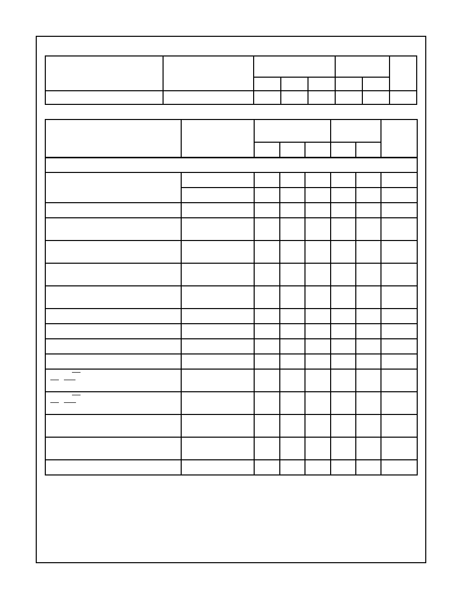
Switching Specifications
V
DD
= V
xHB
= 12V, V
SS
= V
xHS
= 0V, R
DEL
= 10K, Gate Capacitance (C
GATE
) = 1000pF
PARAMETER
TEST CONDITIONS
T
J
= 25
o
C
T
J
= -40
o
C TO
150
o
C
UNITS
MIN
TYP
MAX
MIN
MAX
TURN ON DELAY AND PROPAGATION DELAY
Dead Time
R
DEL
= 100K
3.8
4.5
6
3
7
�s
R
DEL
= 10K
0.38
0.5
0.65
0.3
0.7
�s
Dead Time Channel Matching
R
DEL
= 10K
-
7
15
-
20
%
Lower Turn-Off Propagation Delay
(xLI-xLO)
No Load
-
25
50
-
70
ns
Upper Turn-Off Propagation Delay
(xHI-xHO)
No Load
-
55
80
-
100
ns
Lower Turn-On Propagation Delay
(xLI-xLO)
No Load
-
40
85
-
100
ns
Upper Turn-On Propagation Delay
(xHI-xHO)
No Load
-
75
110
-
150
ns
Rise Time
C
GATE
= 1000pF
-
20
40
-
50
ns
Fall Time
C
GATE
= 1000pF
-
10
20
-
25
ns
Turn-On Input Pulse Width
50
-
-
50
-
ns
Turn-Off Input Pulse Width
50
-
-
50
-
ns
Disable (EN) Turn-Off Propagation Delay
(EN - xLO)
-
50
80
90
ns
Disable (EN) Turn-Off Propagation Delay
(EN - xHO)
-
75
100
-
125
ns
Enable to Lower Turn-On Propagation Delay
(EN - xLO)
-
50
80
-
100
ns
Enable to Upper Turn-On Propagation Delay
(EN- xHO)
R
DEL
= 10K
-
1.2
2
-
3
�s
Refresh Pulse Width (xLO)
375
580
900
350
950
�s
Electrical Specifications
V
DD
= V
xHB
= 12V, V
SS
= V
xHS
= 0V, R
DEL
= 20K, UVLO/EN =
, Gate Capacitance (C
GATE
) = 1000pF
PARAMETER
TEST CONDITIONS
T
J
= 25
o
C
T
J
= -40
o
C TO
150
o
C
UNITS
MIN
TYP
MAX
MIN
MAX
HIP4084
5
HIP4084
NOTES:
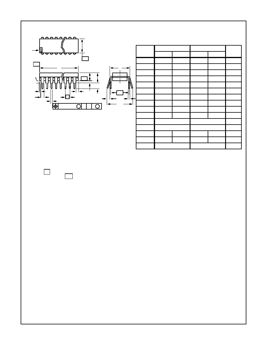
1. Controlling Dimensions: INCH. In case of conflict between
English and Metric dimensions, the inch dimensions control.
2. Dimensioning and tolerancing per ANSI Y14.5M-1982.
3. Symbols are defined in the "MO Series Symbol List" in Section
2.2 of Publication No. 95.
4. Dimensions A, A1 and L are measured with the package seated
in JEDEC seating plane gauge GS-3.
5. D, D1, and E1 dimensions do not include mold flash or protru-
sions. Mold flash or protrusions shall not exceed 0.010 inch
(0.25mm).
6. E and
are measured with the leads constrained to be per-
pendicular to datum
.
7. e
B
and e
C
are measured at the lead tips with the leads uncon-
strained. e
C
must be zero or greater.
8. B1 maximum dimensions do not include dambar protrusions.
Dambar protrusions shall not exceed 0.010 inch (0.25mm).
9. N is the maximum number of terminal positions.
10. Corner leads (1, N, N/2 and N/2 + 1) for E8.3, E16.3, E18.3,
E28.3, E42.6 will have a B1 dimension of 0.030 - 0.045 inch
(0.76 - 1.14mm).
CL
E
e
A
C
e
B
e
C
-B-
E1
INDEX
1 2 3
N/2
N
AREA
SEATING
BASE
PLANE
PLANE
-C-
D1
B1
B
e
D
D1
A
A2
L
A1
-A-
0.010 (0.25)
C A
M
B S
e
A
-C-
Dual-In-Line Plastic Packages (PDIP)
E28.6
(JEDEC MS-011-AB ISSUE B)
28 LEAD DUAL-IN-LINE PLASTIC PACKAGE
SYMBOL
INCHES
MILLIMETERS
NOTES
MIN
MAX
MIN
MAX
A
-
0.250
-
6.35
4
A1
0.015
-
0.39
-
4
A2
0.125
0.195
3.18
4.95
-
B
0.014
0.022
0.356
0.558
-
B1
0.030
0.070
0.77
1.77
8
C
0.008
0.015
0.204
0.381
-
D
1.380
1.565
35.1
39.7
5
D1
0.005
-
0.13
-
5
E
0.600
0.625
15.24
15.87
6
E1
0.485
0.580
12.32
14.73
5
e
0.100 BSC
2.54 BSC
-
e
A
0.600 BSC
15.24 BSC
6
e
B
-
0.700
-
17.78
7
L
0.115
0.200
2.93
5.08
4
N
28
28
9
Rev. 0 12/93