 | –≠–ª–µ–∫—Ç—Ä–æ–Ω–Ω—ã–π –∫–æ–º–ø–æ–Ω–µ–Ω—Ç: HIP5061DS | –°–∫–∞—á–∞—Ç—å:  PDF PDF  ZIP ZIP |

7-53
CAUTION: These devices are sensitive to electrostatic discharge; follow proper IC Handling Procedures.
407-727-9207
|
Copyright
©
Intersil Corporation 1999
HIP5061
7A, High Efficiency Current
Mode Controlled PWM Regulator
Description
The HIP5061 is a complete power control IC, incorporating
both the high power DMOS transistor, CMOS logic and low
level analog circuitry on the same Intelligent Power IC. The
standard "Boost", "Buck-Boost", "Cuk", "Forward", "Flyback"
and the "SEPIC" (Single-Ended Primary Inductance Con-
verter) power supply topologies may be implemented with
this single control IC.
Over-temperature and rapid short-circuit recovery circuitry is
incorporated within the IC. These protection circuits disable
the drive to the power transistor to protect the transistor and
insure rapid restarting of the supply after the short circuit is
removed.
As a result of the power DMOS transistors current (7A at 30%
duty cycle, 5A DC) and 60V capability, supplies with output
power over 50W are possible.
Ordering Information
PART
NUMBER
TEMPERATURE
RANGE
PACKAGE
HIP5061DS
0
o
C to +85
o
C
7 Lead Staggered "Gullwing" SIP
Features
∑ Single Chip Current Mode Control IC
∑ 60V, On-Chip DMOS Power Transistor
∑ Thermal Protection
∑ Over-Current Protection
∑ 250kHz Operation
∑ Output Rise and Fall Times - 10ns
∑ On-Chip Reference Voltage - 5.1V
∑ Slope Compensation
∑ V
DD
Clamp Allows 10.8V to 60V Supply
∑ Supply Current Does Not Increase When Power
Device is On
Applications
∑ Distributed / Board Mounted Power Supplies
∑ DC - DC Converter Modules
∑ Voltage Inverters
∑ Small Uninterruptable Power Supplies
∑ Cascode Switching for Off Line SMPS
File Number
3390.2
April 1994
Pinout
HIP5061 (SIP)
TOP VIEW
PIN 7 V
DD
PIN 6 V
G
PIN 5 DRAIN
PIN 4 SOURCE
PIN 3 FB
PIN 2 V
C
PIN 1 GND
(TAB)
SOURCE
DO NOT
USE
Simplified Functional Diagram
SLOPE
COMPENSATION
5.1V
REFERENCE
GATE
DRIVER
CONTROL
LOGIC
V
DD
CLAMP
V
DD
HIP5061
CLOCK
OVER
TEMP
UNDER
VOLTAGE
V/I
AMP
V
C
FB
GND
DRAIN
V
G
SOURCE
V
OUT
V
IN
2.5V
(TAB)
7-54
Specifications HIP5061
Absolute Maximum Ratings
(Note 1)
Thermal Information
DC Supply Voltage, V
DD
. . . . . . . . . . . . . . . . . . . . . . . . -0.3V to 16V
DC Supply Current, I
DD
. . . . . . . . . . . . . . . . . . . . . . . . . . . . . 105mA
DMOS Drain Voltage . . . . . . . . . . . . . . . . . . . . . . . . . . -0.3V to 60V
Average DMOS Drain Current . . . . . . . . . . . . . . . . . . . . . . . . . . . 5A
DMOS Source Voltage, V
SOURCE
, TAB . . . . . . . . . . . . -0.1V to 0.1V
DC Supply Voltage, V
G
. . . . . . . . . . . . . . . . . . . .-0.3V to V
DD
+ 0.3V
Compensation Pin Current, I
VC
. . . . . . . . . . . . . . . . . -5mA to 35mA
Voltage at All Other Pins. . . . . . . . . . . . . . . . . . .-0.3V to V
DD
+ 0.3V
Operating Junction Temperature Range. . . . . . . . . . . 0
o
C to +105
o
C
Storage Temperature Range . . . . . . . . . . . . . . . . . -55
o
C to +150
o
C
ESD Classification . . . . . . . . . . . . . . . . . . . . . . . . . . . Class 2 - 2KV
Single Pulse Avalanche Energy Rating,
µ
s (Note 2) . . . EAS 100mJ
Thermal Resistance
JC
Plastic SIP Package . . . . . . . . . . . . . . . . . . . . . . . .
2
o
C/W
Maximum Package Power Dissipation at +85
o
C
(Depends Upon Mounting, Heat Sink and Application) . . . . . 10W
Max. Junction Temperature. . . . . . . . . . . . . . . . . . . . . . . . . . +105
o
C
(Controlled By Thermal Shutdown Circuit)
Lead Temperature (Soldering 10s) . . . . . . . . . . . . . . . . . . . . +265
o
C
CAUTION: Stresses above those listed in "Absolute Maximum Ratings" may cause permanent damage to the device. This is a stress only rating and operation
of the device at these or any other conditions above those indicated in the operational sections of this specification is not implied.
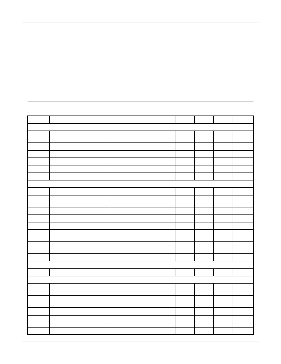
Electrical Specifications
V
DD
= V
G
=12V, V
C
= 5V, V
FB
= 5.1V, SOURCE = GND = DRAIN = 0V, T
J
= 0
o
C to +105
o
C,
Unless Otherwise Specified
SYMBOL
PARAMETER
TEST CONDITIONS
MIN
TYP
MAX
UNITS
DEVICE PARAMETERS
I
DD
Quiescent Supply Current
V
DD
= V
G
= 13.2V, V
C
= 0V,
V
FB
= 4V
6
12
18
mA
I
DD
Operating Supply Current
V
DD
= V
G
= 13.2V, V
C
= 8.5V, V
FB
= 4V
-
24
31
mA
IV
G
Quiescent Current to Gate Driver
V
DD
= V
G
= 13.2V, V
C
= 0V
-
0
10
µ
A
IV
G
Operating Current to Gate Driver
V
C
= 3V
-
1
2
mA
V
DDC
Clamp Voltage
I
DD
= 100mA
13.3
14
15
V
V
REF
Reference Voltage
I
VC
= 0
µ
A, V
C
= V
FB
5.0
5.1
5.2
V
AMPLIFIERS
|I
FB
|
Input Current
V
FB
= V
REF
-
-0.85
0.5
µ
A
g
m
(V
FB
)
V
FB
Transconductance
I
VC
/(V
FB
- V
REF
)
/I
VC
/ = 500
µ
A, Note 3
20
30
43
mS
IV
CMAX
Maximum Source Current
V
FB
= 4.6V
-4
-1.8
-1
mA
IV
CMAX
Maximum Sink Current
V
FB
= 5.6V
1
1.8
4
mA
A
OL
Voltage Gain
/I
VC
/ = 500
µ
A, Note 3
44
50
-
dB
V
CMAX
Short Circuit Recovery Compara-
tor Rising Threshold Voltage
5.4
6.6
8.9
V
V
CHYS
Short Circuit Recovery
Comparator Hysteresis Voltage
0.7
1.1
1.8
V
IVC
OVER
V
C
Over-Voltage Current
V
DD
= V
G
= 10.8V, V
C
= V
CMAX
0
10
25
mA
CLOCK
fq
Internal Clock Frequency
210
250
290
kHz
DMOS TRANSISTOR
r
DS
(ON)
Drain-Source On-State
Resistance
I
DRAIN
= 5A, V
DD
= V
G
= 10.8V
T
J
= +25
o
C
-
0.15
0.22
r
DS
(ON)
Drain-Source On-State
Resistance
I
DRAIN
= 5A, V
DD
= V
G
= 10.8V
T
J
= +105
o
C
-
-
0.33
I
DSS
Drain-Source Leakage Current
V
DRAIN
= 60V
-
0.5
10
µ
A
I
DSH
Average Drain Short Circuit
Current
V
DRAIN
= 5V, Note 4
-
-
5
A
C
DRAIN
DRAIN Capacitance
Note 4
-
200
-
pF
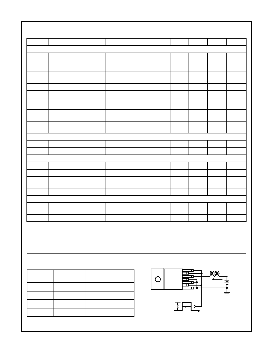
7-55
Specifications HIP5061
CURRENT CONTROLLED PWM
g
m
(V
C
)
I
DRAIN, PEAK
/
V
C
Note 3
1.4
2.2
3.0
A/V
V/I
REF
Voltage to Current Converter Ref-
erence Voltage
I
DRAIN
= 0.25A, Note 3
2.4
2.8
3.1
V
t
BT
Current Comparator Blanking
Time
Note 3
40
100
175
ns
t
ONMIN
Minimum DMOS "ON" Time
Note 3
60
150
250
ns
t
OFFMIN
Minimum DMOS "OFF" Time
Note 3
40
125
200
ns
MinCI
Minimum Controllable DMOS
Peak Current
Note 3
-
100
250
mA
MaxCI
Maximum Controllable DMOS
Peak Current
Duty Cycle = 6% to 30%, Note 3
7
9.5
12
A
MaxCI
Maximum Controllable DMOS
Peak Current
Duty Cycle = 30% to 96%, Note 3
5
8
12
A
CURRENT COMPENSATION RAMP
I/
t
Compensation Ramp Rate
I
DRAIN, PEAK
/
Time, Note 3
-1.4
-0.85
-0.45
A/
µ
s
t
RD
Compensation Ramp Delay
Note 3
1.3
1.5
1.8
µ
s
START-UP
V
DDMIN
Rising V
DD
Threshold Voltage
V
FB
= 4V
9.3
10.3
10.8
V
V
DDHYS
Power-On Hysteresis
V
FB
= 4V
0.3
0.45
0.6
V
V
CEN
Enable Comparator Threshold
Voltage
1.0
1.5
2.0
V
R
VC
Power-Up Resistance
4V < V
DD
< 10.8V, V
C
= 0.8V
50
500
3000
THERMAL MONITOR
T
J
Substrate Temperature for
Thermal Monitor to Trip
Note 4
105
-
145
o
C
T
JHY
Temperature Hysteresis
Note 4
-
5
-
o
C
NOTES:
1. All Voltages relative to pin 1, GND.
2. V
D
= 10V, Starting T
J
= +25
o
C, L = 4mH, I
PEAK
= 7A.
3. Test is performed at wafer level only.
4. Determined by design, not a measured parameter.
Electrical Specifications
V
DD
= V
G
=12V, V
C
= 5V, V
FB
= 5.1V, SOURCE = GND = DRAIN = 0V, T
J
= 0
o
C to +105
o
C,
Unless Otherwise Specified (Continued)
SYMBOL
PARAMETER
TEST CONDITIONS
MIN
TYP
MAX
UNITS
TABLE 1.
CONDITIONS FOR UNCLAMPED ENERGY CIRCUIT
V
D
(V)
I
L
(PEAK AMPS)
L (mH)
EAS (mJ)
10
5
40
550
10
7
4TZ
120
6
10
0.33
18
6
12.5
0.14
12
NOTE:
Device Selected to Obtain Peak Current without Clocking
FIGURE 1. UNCLAMPED ENERGY TEST CIRCUIT
VARY t
P
TO OBTAIN
REQUIRED PEAK I
L
12V
t
P
7
1
I
L
V
D
+
-
L
HIP5061

7-56
HIP5061
Definitions of Electrical Specifications
Refer to the Functional Block Diagram of Figure 1 for loca-
tions of functional blocks and devices.
Device Parameters
I
DD
, Quiescent Supply Current - Supply current with the
chip disabled. The Clock, Error Amplifier, Voltage-to-Current
Converter, and Current Ramp circuits draw only quiescent
current. The supply voltage must be kept lower than the
turn-on voltage of the V
DD
clamp or else the supply current
increases dramatically.
I
DD
, Operating Supply Current - Supply current with the
chip enabled. The Error Amplifier is drawing its maximum
current because V
FB
is less than its reference voltage. The
voltage-to-current amplifier is drawing its maximum because
V
C
is at its maximum. The ramp circuit is drawing its maxi-
mum because it is not being disabled by the DMOS transis-
tor turning off.
IV
G
, Quiescent Gate Driver Current - Gate Drivers supply
current with the IC disabled. The Gate Driver is not toggling
and so it draws only leakage current.
IV
G
, Operating Gate Driver Current - Gate Drivers supply
current with the IC enabled. The DMOS transistor drain is
loaded with a large resistor tied to 60V so that it is swinging
from 0V to 60V during each cycle.
V
DDC
, V
DD
Clamp - V
DD
voltage at the maximum allowed
current through the V
DD
Clamp.
V
REF
, Reference Voltage - The voltage on FB that sets the
current on V
C
to zero. This is the reference voltage for the
DC/DC converter.
Amplifiers
|I
FB
|, Input Current - Current through FB pin when it is at its
normal operating voltage. This current must be considered
when connecting the output of a DC/DC convertor to the FB
pin via a resistor divider.
g
m
(V
FB
), Transconductance - The change in current
through the V
C
pin divided by the change in voltage on FB.
The g
m
times the resistance between V
C
and ground gives
the voltage gain of the Error Amplifier.
IV
CMAX
, Maximum Source Current - The current on V
C
when FB is more than a few hundred millivolts less than
V
REF
.
IV
CMAX
, Maximum Sink Current - The current on V
C
when
FB is more than a few hundred millivolts more than V
REF
.
A
OL
, Voltage Gain - Change in the voltage on V
C
divided by
the change in voltage on FB. There is no resistive load on
V
C
. This is the voltage gain of the error amplifier when g
m
times load resistance is larger than this gain.
V
CMAX
, V
C
Rising Threshold - The voltage on V
C
that
causes the Voltage-to-Current Amplifier to reach full-scale.
When V
C
reaches this voltage, the V
C
NMOS transistor (tran-
sistor with its drain connected to the V
C
pin in the Functional
Block Diagram of Figure 2) turns on and tries to lower the volt-
age on V
C
.
V
CHYS
, V
CMAX
Hysteresis - The voltage on V
C
that causes
the NMOS transistor to turnoff if it had been turned on by V
C
exceeding V
CMAX
. At this voltage the current out of the Voltage-
to-Current Converter is at roughly three quarters of full-scale.
IVC
OVER
, V
C
Over-Voltage Current - The current drawn
through the V
C
pin after the NMOS transistor is turned on
due to excessive voltage on V
C
. The NMOS transistor con-
nected to the V
C
pin draws more than enough current to
overcome the full scale source current of the Error Amplifier.
Clock
fq, Frequency - The frequency of the DC/DC converter. The
Clock actually runs faster than this value so that various con-
trol signals can be internally generated.
DMOS Transistor
r
DS(ON)
, "On" Resistance - Resistance from DMOS transis-
tor Drain to Source at maximum drain current and minimum
Gate Driver voltage, V
G
.
I
DSS
, Leakage Current - Current through DMOS transistor
at the Maximum Rated Voltage.
Current Controlled PWM
g
m
(V
C
), Transconductance - The change in the DMOS tran-
sistor peak drain current divided by the change in voltage on
V
C
. When analyzing DC/DC converters the DMOS transistor
and the inductor tied to the drain are sometimes modelled as
a voltage-controlled current source and this parameter is the
gain of the voltage-controlled current source.
V/I
REF
, Current Control Threshold - The voltage on V
C
that causes the DMOS transistor to shut off at the minimum
controllable current. This voltage is greater than the Enable
Comparator Threshold (V
CEN
) so that as V
C
rises the IC
does not jump from the disabled state to the DMOS transis-
tor conducting a large current.
t
BT
, Blanking Time - At the beginning of each cycle there is
a blanking time that the DMOS transistor turns-on and stays-
on no matter how high drain the current. This blanking time
permits ringing in the external parasitic capacitances and
inductances to dampen and for the charging of the reverse
bias on the rectifier diode.
t
ONMIN
, Minimum DMOS Transistor "On" Time - The mini-
mum on-time for the DMOS transistor where small changes
in the V
C
voltage make predictable changes in the DMOS
transistor peak current. Converters should be designed to
avoid requiring pulse widths less than the minimum on time.
t
OFFMIN
, Minimum DMOS Transistor "Off" Time - The min-
imum off-time for the DMOS transistor that allows enough time
for the IC to get ready for the next cycle. Converters should be
designed to avoid requiring pulse widths so large that the mini-
mum off time is violated. (However, zero off time is allowed, that
is, the DMOS transistor can stay on from one cycle to the next.)
MinCI, Minimum Controllable Current - When the voltage
on V
C
is below V/I
REF
, the peak current for the DMOS tran-
sistor is too small for the Current Comparator to operate reli-
ably. Converters should be designed to avoid operating the
DMOS transistor at this low current.
7-57
HIP5061
MaxCI, Maximum Controllable Current - The peak current
for the DMOS transistor when the Voltage-to-Current Con-
verter is at its full scale output. The DMOS transistor current
may exceed this value during the blanking time so proper
precautions should be taken. This parameter is unchanged
for the first 3/8 of the cycle and then decreases linearly with
time because of the Current Ramp becoming active.
Current Compensation Ramp
I/
t, Compensation Ramp Rate - At a given voltage on V
C
the DMOS transistor will turn off at some current that stays
constant for about the first 1.5
µ
s of the cycle. After 1.5
µ
s, the
turnoff current starts to linearly decrease. This parameter
specifies the change in the DMOS transistor turnoff current.
t
RD
, Compensation Ramp Delay - The time into each cycle
that the compensation ramp turns on. The Current Compen-
sation Ramp, used for Slope Compensation, is developed by
the Current Ramp block shown in the FUNCTIONAL BLOCK
DIAGRAM of Figure 2.
Start-Up
V
DDMIN
, Rising V
DD
Threshold Voltage - The minimum
voltage on V
DD
needed to enable the IC.
V
DDHYS
, Power - On Hysteresis Voltage - The difference
between the voltage on V
DD
that enables the IC and the volt-
age that disables the IC.
V
CEN
, Enable Comparator Threshold Voltage - The mini-
mum voltage on V
C
needed to enable the IC. The IC can be
shutdown from an open-collector logic gate by pulling down
the V
C
pin to GND.
R
VC
, Power - Up Resistance - When V
DD
is below V
DDMIN
,
the NMOS transistor connected to the V
C
pin is turned on to
make sure the V
C
node is low. Thus the voltage on V
C
can
gradually build up as will the trip current on the DMOS tran-
sistor. This is the only form of "soft start" included on the IC.
The resistance is measured between the V
C
and GND pins.
Thermal Monitor
T
J
, Rising Temperature Threshold - The IC temperature
that causes the IC to disable itself so as to prevent damage.
Proper heat-sinking is required to avoid over-temperature
conditions, especially during start-up when the DMOS tran-
sistor may stay on for a long time if an external soft-start cir-
cuit is not added.
T
JHY
, Temperature Hysteresis - The IC must cool down
this much after it is disabled by being too hot before it can
resume normal operation.
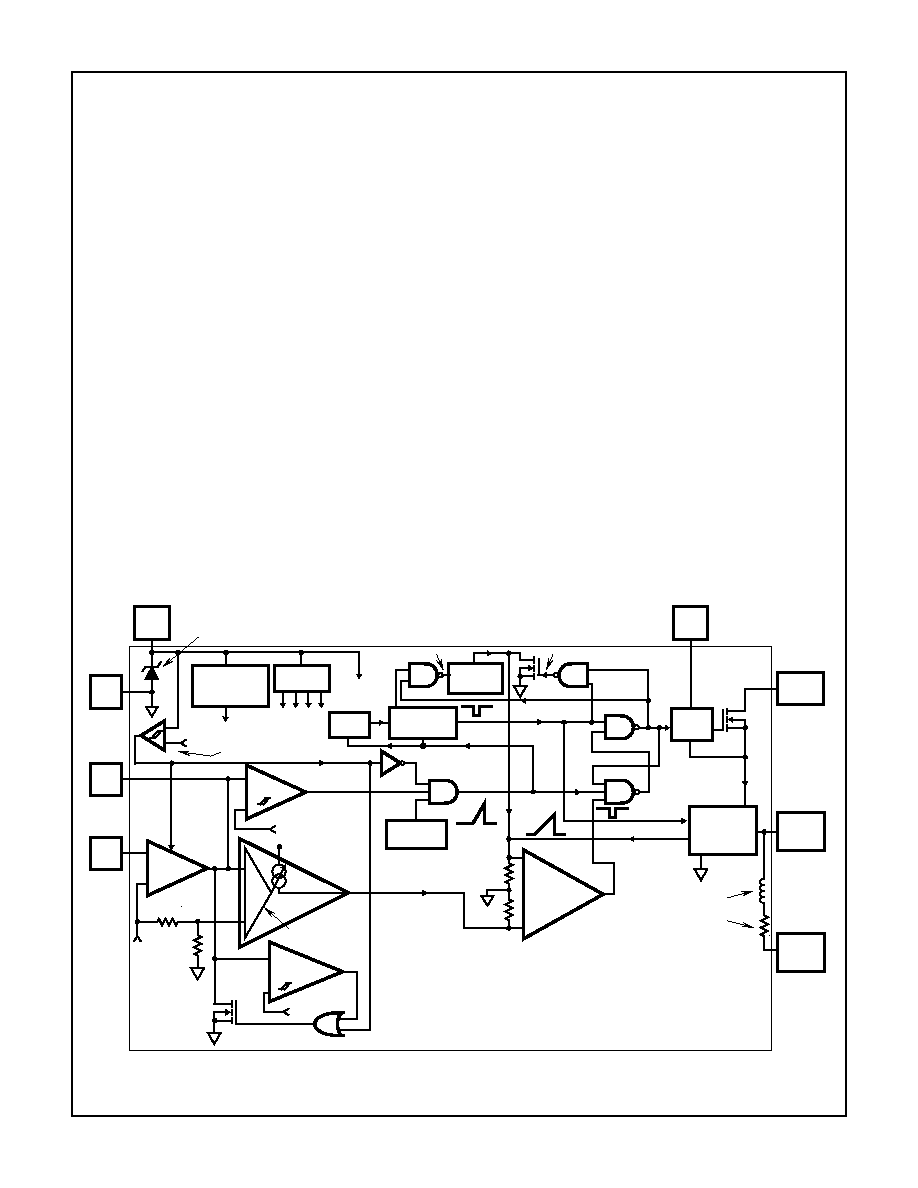
FIGURE 2. FUNCTIONAL BLOCK DIAGRAM OF THE HIP5061
GATE
DRIVER
BIAS
CURRENT
MONITORING
V
G
V
REF
= 5.1V
V
DD
V
DD
SOURCE
DRAIN
7
TAB
6
5
CIRCUITS
+
-
+
-
SOURCE
CONTROL
CLOCK
4
ENABLE
ERROR
AMP
THERMAL
MONITOR
RAMP
CURRENT
COMPARE
1.5V
5.1V
2K
360
HIP5061
CURRENT
+
-
+
-
7.0V
SHORT
V
DD
MONITOR
10.3V
+
-
BLANKING
ENABLE
2K
CURRENT SAMPLE
RAMP ENABLE
RAMP RESET
ERROR CURRENT
100ns
UNDER VOLTAGE
V
DD
ERROR
DISABLE
GND
1
V
REF
AMP
360
CIRCUIT
LOGIC
INTERNAL LEAD
INDUCTANCE
AND RESISTANCE
LOCK OUT
V
C
2
FB
3
V
DD
CLAMP
BAND GAP
REFERENCE
REGULATOR
+
-
VOLTAGE TO
CURRENT
CONVERTER
LIGHT LOAD
COMPARATOR