 | –≠–ª–µ–∫—Ç—Ä–æ–Ω–Ω—ã–π –∫–æ–º–ø–æ–Ω–µ–Ω—Ç: HIP6015 | –°–∫–∞—á–∞—Ç—å:  PDF PDF  ZIP ZIP |
1
File Number
4421.2
HIP6015
Buck Pulse-Width Modulator (PWM)
Controller and Output Voltage Monitor
The HIP6015 provides complete control and protection for a
DC-DC converter optimized for high-performance
microprocessor applications. It is designed to drive an
N-Channel MOSFET in a standard buck topology. The
HIP6015 integrates all of the control, output adjustment,
monitoring and protection functions into a single package.
The output voltage of the converter is easily adjusted and
precisely regulated. The HIP6015 includes a fully
TTL-compatible 5-input digital-to-analog converter (DAC)
that adjusts the output voltage from 2.1V
DC
to 3.5V
DC
in
0.1V increments and from 1.8V
DC
to 2.05V
DC
in 0.05V
steps. The precision reference and voltage-mode regulator
hold the selected output voltage to within
±
1% over
temperature and line voltage variations.
The HIP6015 provides simple, single feedback loop,
voltage-mode control with fast transient response. It
includes a 200kHz free-running triangle-wave oscillator that
is adjustable from below 50kHz to over 1MHz. The error
amplifier features a 15MHz gain-bandwidth product and
6V/
µ
s slew rate which enables high converter bandwidth for
fast transient performance. The resulting PWM duty ratio
ranges from 0% to 100%.
The HIP6015 monitors the output voltage with a window
comparator that tracks the DAC output and issues a Power
Good signal when the output is within
±
10%. The HIP6015
protects against over-current and over-voltage conditions by
inhibiting PWM operation. Additional built-in over-voltage
protection triggers an external SCR to crowbar the input
supply. The HIP6015 monitors the current by using the
r
DS(ON)
of the upper MOSFET which eliminates the need for
a current sensing resistor.
Pinout
HIP6015
(SOIC)
TOP VIEW
Features
∑ Drives N-Channel MOSFET
∑ Operates from +5V or +12V Input
∑ Simple Single-Loop Control Design
- Voltage-Mode PWM Control
∑ Fast Transient Response
- High-Bandwidth Error Amplifier
- Full 0% to 100% Duty Ratio
∑ Excellent Output Voltage Regulation
-
±
1% Over Line Voltage and Temperature
∑ TTL-Compatible 5-Bit Digital-to-Analog Output Voltage
Selection
- Wide Range . . . . . . . . . . . . . . . . . . . 1.8V
DC
to 3.5V
DC
- 0.1V Binary Steps . . . . . . . . . . . . . . . 2.1V
DC
to 3.5V
DC
- 0.05V Binary Steps . . . . . . . . . . . . . 1.8V
DC
to 2.05V
DC
∑ Power-Good Output Voltage Monitor
∑ Over-Voltage and Over-Current Fault Monitors
- Does Not Require Extra Current Sensing Element,
Uses MOSFET's r
DS(ON)
∑ Small Converter Size
- Constant Frequency Operation
- 200kHz Free-Running Oscillator Programmable from
50kHz to over 1MHz
Applications
∑ Power Supply for PentiumÆ, Pentium Pro, Pentium II,
PowerPCTM, K6TM, 6X86TM and AlphaTM Microprocessors
∑ High-Power 5V to 3.xV DC-DC Regulators
∑ Low-Voltage Distributed Power Supplies
6X86TM is a trademark of Cyrix Corporation.
AlphaTM is a trademark of Digital Equipment Corporation.
K6TM is a trademark of Advanced Micro Devices, Inc.
PentiumÆ is a registered trademark of Intel Corporation.
PowerPCTM is a trademark of IBM.
11
12
13
14
15
16
17
18
20
19
10
9
8
7
6
5
4
3
2
1
V
SEN
OCSET
SS
VID0
VID1
VID2
VID4
VID3
COMP
FB
R
T
V
CC
NC
NC
OVP
BOOT
UGATE
PHASE
PGOOD
GND
Ordering Information
PART NUMBER
TEMP.
RANGE (
o
C)
PACKAGE
PKG.
NO.
HIP6015CB
0 to 70
20 Ld SOIC
M20.3
Data Sheet
March 2000
CAUTION: These devices are sensitive to electrostatic discharge; follow proper IC Handling Procedures.
1-888-INTERSIL or 321-724-7143
|
Copyright
©
Intersil Corporation 2000
2
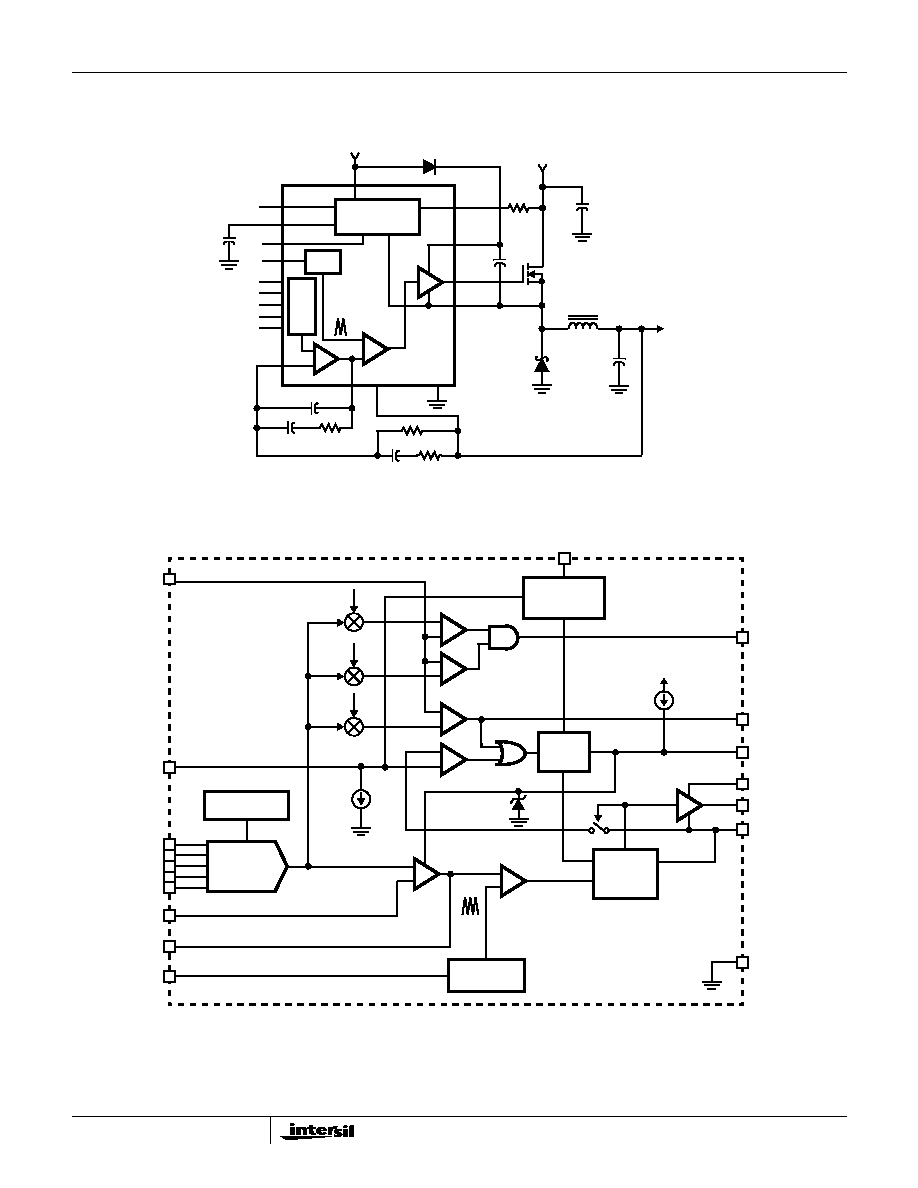
Typical Application
Block Diagram
+
-
+
-
+12V
+V
OUT
HIP6015
V
SEN
R
T
FB
COMP
SS
PGOOD
GND
MONITOR AND
PROTECTION
OSC
UGATE
OCSET
PHASE
BOOT
V
CC
V
IN
= +5V OR +12V
OVP
VID0
VID1
VID2
VID3
D/A
VID4
D/A
CONVERTER
(DAC)
OSCILLATOR
SOFT-
START
REFERENCE
POWER-ON
RESET (POR)
115%
110%
90%
INHIBIT
PWM
COMPARATOR
ERROR
AMP
V
CC
PGOOD
SS
PWM
OVP
R
T
GND
V
SEN
OCSET
VID0
VID1
VID2
VID3
FB
COMP
DACOUT
OVER-
VOLTAGE
OVER-
CURRENT
GATE
CONTROL
LOGIC
BOOT
UGATE
PHASE
200
µ
A
10
µ
A
4V
+
-
+
-
+
-
+
-
+
-
+
-
VID4
HIP6015

3
Absolute Maximum Ratings
Thermal Information
Supply Voltage, V
CC
. . . . . . . . . . . . . . . . . . . . . . . . . . . . . . . . +15V
Boot Voltage, V
BOOT
- V
PHASE
. . . . . . . . . . . . . . . . . . . . . . . . +15V
Input, Output or I/O Voltage . . . . . . . . . . . . GND -0.3V to V
CC
+0.3V
ESD Classification . . . . . . . . . . . . . . . . . . . . . . . . . . . . . . . . . Class 2
Operating Conditions
Supply Voltage, V
CC
. . . . . . . . . . . . . . . . . . . . . . . . . . . +12V
±
10%
Ambient Temperature Range . . . . . . . . . . . . . . . . . . . . . 0
o
C to 70
o
C
Junction Temperature Range . . . . . . . . . . . . . . . . . . . . 0
o
C to 125
o
C
Thermal Resistance (Typical, Note 1)
JA
(
o
C/W)
SOIC Package. . . . . . . . . . . . . . . . . . . . . . . . . . . . .
118
Maximum Junction Temperature (Plastic Package) . . . . . . . .150
o
C
Maximum Storage Temperature Range . . . . . . . . . . -65
o
C to 150
o
C
Maximum Lead Temperature (Soldering 10s) . . . . . . . . . . . . .300
o
C
(SOIC - Lead Tips Only)
CAUTION: Stresses above those listed in "Absolute Maximum Ratings" may cause permanent damage to the device. This is a stress only rating and operation of the
device at these or any other conditions above those indicated in the operational sections of this specification is not implied.
NOTE:
1.
JA
is measured with the component mounted on a low effective thermal conductivity test board in free air. See Tech Brief 379 for details.
Electrical Specifications
Recommended Operating Conditions, Unless Otherwise Noted
PARAMETER
SYMBOL
TEST CONDITIONS
MIN
TYP
MAX
UNITS
V
CC
SUPPLY CURRENT
Nominal Supply
I
CC
UGATE Open
-
5
-
mA
POWER-ON RESET
Rising V
CC
Threshold
V
OCSET
= 4.5V
-
-
10.4
V
Falling V
CC
Threshold
V
OCSET
= 4.5V
8.2
-
-
V
Rising V
OCSET
Threshold
-
1.26
-
V
OSCILLATOR
Free Running Frequency
R
T
= Open
185
200
215
kHz
Total Variation
6k
< R
T
to GND < 200k
-15
-
+15
%
Ramp Amplitude
V
OSC
R
T
= Open
-
1.9
-
V
P-P
REFERENCE AND DAC
DAC (VID0-VID4) Input Low Voltage
-
-
0.8
V
DAC (VID0-VID4) Input High Voltage
2.0
-
-
V
DACOUT Voltage Accuracy
-1.0
-
+1.0
%
ERROR AMPLIFIER
DC Gain
-
88
-
dB
Gain-Bandwidth Product
GBW
-
15
-
MHz
Slew Rate
SR
COMP = 10pF
-
6
-
V/
µ
s
GATE DRIVER
Upper Gate Source
I
UGATE
V
BOOT
- V
PHASE
= 12V, V
UGATE
= 6V
350
500
-
mA
Upper Gate Sink
RUGATE
-
5.5
10
PROTECTION
Over-Voltage Trip (V
SEN
/DACOUT)
-
115
120
%
OCSET Current Source
I
OCSET
V
OCSET
= 4.5V
170
200
230
µ
A
OVP Sourcing Current
I
OVP
V
SEN
= 5.5V; V
OVP
= 0V
60
-
-
mA
Soft Start Current
I
SS
-
10
-
µ
A
HIP6015
4
Functional Pin Description
V
SEN
(Pin 1)
This pin is connected to the converters output voltage. The
PGOOD and OVP comparator circuits use this signal to
report output voltage status and for overvoltage protection.
OCSET (Pin 2)
Connect a resistor (R
OCSET
) from this pin to the drain of the
upper MOSFET. R
OCSET
, an internal 200
µ
A current source
(I
OCS
), and the upper MOSFET on-resistance (r
DS(ON)
) set
the converter over-current (OC) trip point according to the
following equation:
An over-current trip cycles the soft-start function.
SS (Pin 3)
Connect a capacitor from this pin to ground. This capacitor,
along with an internal 10
µ
A current source, sets the soft-
start interval of the converter.
VID0-4 (Pins 4-8)
VID0-4 are the input pins to the 5-bit DAC. The states of
these five pins program the internal voltage reference
(DACOUT). The level of DACOUT sets the converter output
voltage. It also sets the PGOOD and OVP thresholds. Table
1 specifies DACOUT for the 32 combinations of DAC inputs.
COMP (Pin 9) and FB (Pin 10)
COMP and FB are the available external pins of the error
amplifier. The FB pin is the inverting input of the error
amplifier and the COMP pin is the error amplifier output.
These pins are used to compensate the voltage-control
feedback loop of the converter.
POWER GOOD
Upper Threshold (V
SEN
/DACOUT)
V
SEN
Rising
106
-
111
%
Lower Threshold (V
SEN
/DACOUT)
V
SEN
Falling
89
-
94
%
Hysteresis (V
SEN
/DACOUT)
Upper and Lower Threshold
-
2
-
%
PGOOD Voltage Low
V
PGOOD
I
PGOOD
= -5mA
-
0.5
-
V
Electrical Specifications
Recommended Operating Conditions, Unless Otherwise Noted
PARAMETER
SYMBOL
TEST CONDITIONS
MIN
TYP
MAX
UNITS
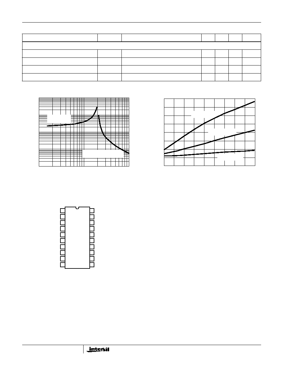
Typical Performance Curves
FIGURE 1. R
T
RESISTANCE vs FREQUENCY
FIGURE 2. BIAS SUPPLY CURRENT vs FREQUENCY
10
100
1000
SWITCHING FREQUENCY (kHz)
RESIST
ANCE (k
)
10
100
1000
R
T
PULLUP
TO +12V
R
T
PULLDOWN TO V
SS
100
200
300
400
500
600
700
800
900
1000
40
35
30
25
20
15
10
5
0
I
CC
(mA)
SWITCHING FREQUENCY (kHz)
C
UGATE
= 3300pF
C
UGATE
= 1000pF
C
UGATE
= 10pF
11
12
13
14
15
16
17
18
20
19
10
9
8
7
6
5
4
3
2
1
V
SEN
OCSET
SS
VID0
VID1
VID2
VID4
VID3
COMP
FB
R
T
V
CC
NC
NC
OVP
BOOT
UGATE
PHASE
PGOOD
GND
I
PEAK
I
OCS
R
OCSET
∑
r
DS ON
(
)
--------------------------------------------
=
HIP6015
5
GND (Pin 11)
Signal ground for the IC. All voltage levels are measured with
respect to this pin.
PGOOD (Pin 12)
PGOOD is an open collector output used to indicate the
status of the converter output voltage. This pin is pulled low
when the converter output is not within
±
10% of the
DACOUT reference voltage. Exception to this behavior are
the cases where the VID pins combination yield a 0V
converter output; in these cases PGOOD asserts a high
level.
PHASE (Pin 13)
Connect the PHASE pin to the upper MOSFET source. This
pin is used to monitor the voltage drop across the MOSFET
for over-current protection. This pin also provides the return
path for the upper gate drive.
UGATE (Pin 14)
Connect UGATE to the upper MOSFET gate. This pin
provides the gate drive for the upper MOSFET.
BOOT (Pin 15)
This pin provides bias voltage to the upper MOSFET driver.
A bootstrap circuit may be used to create a BOOT voltage
suitable to drive a standard N-Channel MOSFET.
NC (Pin 16)
No connection.
NC (Pin 17)
No connection.
V
CC
(Pin 18)
Provide a 12V bias supply for the chip to this pin.
OVP (Pin 19)
The OVP pin can be used to drive an external SCR in the
event of an overvoltage condition. Output rising 15% more
than the DAC-set voltage triggers a high output on this pin
and disables PWM gate drive circuitry.
R
T
(Pin 20)
This pin provides oscillator switching frequency adjustment.
By placing a resistor (R
T
) from this pin to GND, the nominal
200kHz switching frequency is increased according to the
following equation:
Conversely, connecting a pull-up resistor (R
T
) from this pin
to V
CC
reduces the switching frequency according to the
following equation:
Functional Description
Initialization
The HIP6015 automatically initializes upon receipt of power.
Special sequencing of the input supplies is not necessary.
The Power-On Reset (POR) function continually monitors
the input supply voltages. The POR monitors the bias
voltage at the V
CC
pin and the input voltage (V
IN
) on the
OCSET pin. The level on OCSET is equal to V
IN
less a fixed
voltage drop (see over-current protection). The POR function
initiates soft start operation after both input supply voltages
exceed their POR thresholds. For operation with a single
+12V power source, V
IN
and V
CC
are equivalent and the
+12V power source must exceed the rising V
CC
threshold
before POR initiates operation.
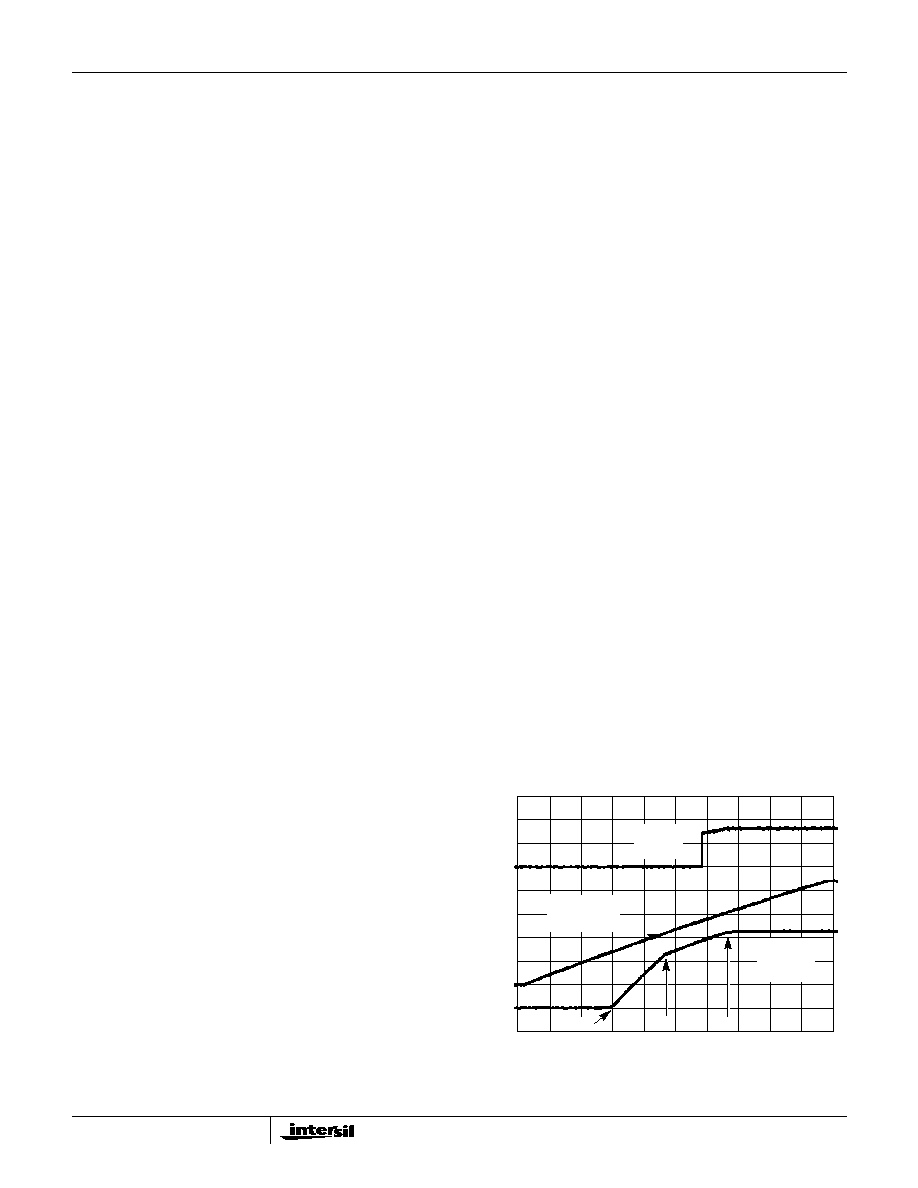
Soft Start
The POR function initiates the soft start sequence. An
internal 10
µ
A current source charges an external capacitor
(C
SS
) on the SS pin to 4V. Soft start clamps the error
amplifier output (COMP pin) and reference input (+ terminal
of error amp) to the SS pin voltage. Figure 3 shows the soft
start interval with C
SS
= 0.1
µ
F. Initially the clamp on the error
amplifier (COMP pin) controls the converter's output voltage.
At t
1
in Figure 3, the SS voltage reaches the valley of the
oscillator's triangle wave. The oscillator's triangular
waveform is compared to the ramping error amplifier voltage.
This generates PHASE pulses of increasing width that
charge the output capacitor(s). This interval of increasing
pulse width continues to t
2
. With sufficient output voltage,
the clamp on the reference input controls the output voltage.
This is the interval between t
2
and t
3
in Figure 3. At t
3
the SS
voltage exceeds the DACOUT voltage and the output
voltage is in regulation. This method provides a rapid and
controlled output voltage rise. The PGOOD signal toggles
`high' when the output voltage (V
SEN
pin) is within
±
5% of
DACOUT. The 2% hysteresis built into the power good
comparators prevents PGOOD oscillation due to nominal
output voltage ripple.
Fs
200kHz
5
10
6
∑
R
T
k
(
)
---------------------
+
(R
T
to GND)
Fs
200kHz
4
10
7
∑
R
T
k
(
)
---------------------
≠
(R
T
to 12V)
0V
0V
0V
TIME (5ms/DIV.)
SOFT-START
(1V/DIV.)
OUTPUT
(1V/DIV.)
VOLTAGE
t
2
t
3
PGOOD
(2V/DIV.)
t
1
FIGURE 3. SOFT START INTERVAL
HIP6015