2-238
HIP6018B
Advanced PWM and Dual Linear Power
Control
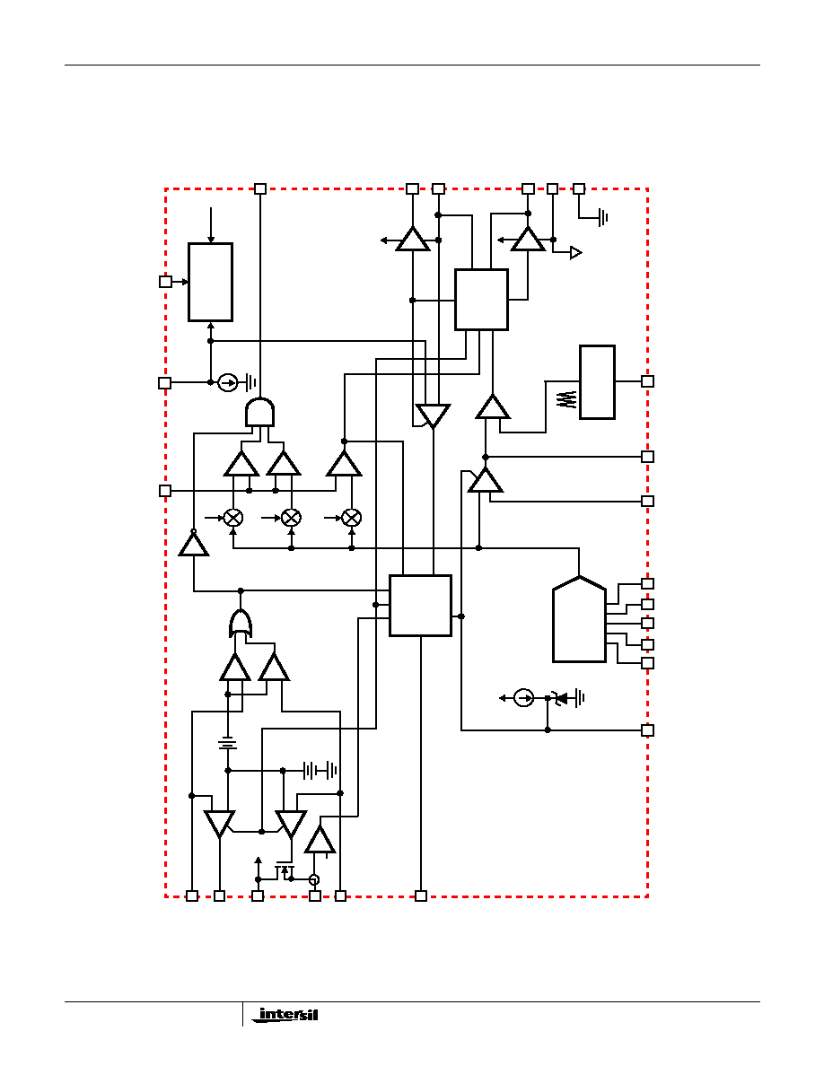
The HIP6018B provides the power control and protection for
three output voltages in high-performance microprocessor
and computer applications. The IC integrates a PWM
controllers, a linear regulator and a linear controller as well
as the monitoring and protection functions into a single
package. The PWM controller regulates the microprocessor
core voltage with a synchronous-rectified buck converter.
The linear controller regulates power for the GTL bus and
the linear regulator provides power for the clock driver circuit.
The HIP6018B includes an Intel-compatible, TTL 5-input
digital-to-analog converter (DAC) that adjusts the core PWM
output voltage from 2.1VDC to 3.5VDC in 0.1V increments
and from 1.3VDC to 2.05VDC in 0.05V steps. The precision
reference and voltage-mode control provide
±
1% static
regulation. The linear regulator uses an internal pass device
to provide 2.5V
±
2.5%. The linear controller drives an
external N-channel MOSFET to provide 1.5V
±
2.5%.
The HIP6018B monitors all the output voltages. A single
Power Good signal is issued when the core is within 10% of
the DAC setting and the other levels are above their under-
voltage levels. Additional built-in over-voltage protection for
the core output uses the lower MOSFET to prevent output
voltages above 115% of the DAC setting. The PWM over-
current function monitors the output current by using the
voltage drop across the upper MOSFET's r
DS(ON)
,
eliminating the need for a current sensing resistor.
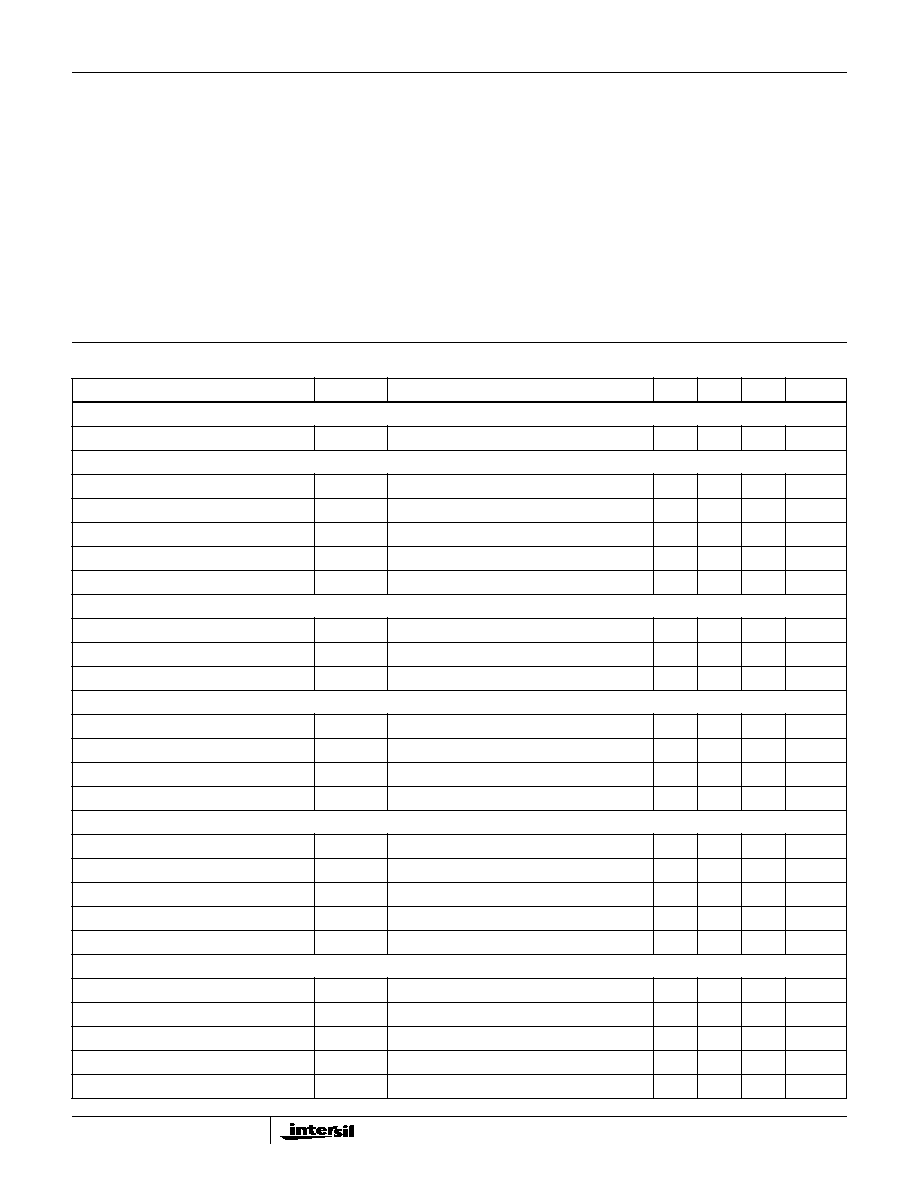
Pinout
HIP6018B
(SOIC)
TOP VIEW
Features
∑ Provides 3 Regulated Voltages
- Microprocessor Core, Clock and GTL Power
∑ Drives N-Channel MOSFETs
∑ Operates from +3.3V, +5V and +12V Inputs
∑ Simple Single-Loop PWM Control Design
- Voltage-Mode Control
∑ Fast Transient Response
- High-Bandwidth Error Amplifier
- Full 0% to 100% Duty Ratios
∑ Excellent Output Voltage Regulation
- Core PWM Output:
±
1% Over Temperature
- Other Outputs:
±
2.5% Over Temperature
∑ TTL-Compatible 5-Bit Digital-to-Analog Core Output
Voltage Selection
- Wide Range . . . . . . . . . . . . . . . . . . . 1.3V
DC
to 3.5V
DC
- 0.1V Steps . . . . . . . . . . . . . . . . . . . . 2.1V
DC
to 3.5V
DC
- 0.05V Steps . . . . . . . . . . . . . . . . . . 1.3V
DC
to 2.05V
DC
∑ Power-Good Output Voltage Monitor
∑ Microprocessor Core Voltage Protection Against Shorted
MOSFET
∑ Over-Voltage and Over-Current Fault Monitors
- Does Not Require Extra Current Sensing Element,
Uses MOSFET's r
DS(ON)
∑ Small Converter Size
- Constant Frequency Operation
- 200kHz Free-Running Oscillator; Programmable from
50kHz to over 1MHz
Applications
∑ Full Motherboard Power Regulation for Computers
∑ Low-Voltage Distributed Power Supplies
VCC
VID4
VID3
VID2
RT
FB2
VIN2
UGATE1
OCSET1
PGND
LGATE1
GND
FB3
VOUT2
PHASE1
24
23
22
21
20
19
18
17
16
15
1
2
3
4
5
6
7
8
9
10
11
12
14
13
FAULT
VID1
SS
FB1
DRIVE3
VID0
PGOOD
VSEN1
COMP1
Ordering Information
PART NUMBER
TEMP.
RANGE (
o
C)
PACKAGE
PKG.
NO.
HIP6018BCB
0 to 70
24 Ld SOIC
M24.3
Data Sheet
May 1999
File Number
4586.1
CAUTION: These devices are sensitive to electrostatic discharge; follow proper IC Handling Procedures.
www.intersil.com or 407-727-9207
|
Copyright
©
Intersil Corporation 1999
2-241
Absolute Maximum Ratings
Thermal Information
Supply Voltage, V
CC
. . . . . . . . . . . . . . . . . . . . . . . . . . . . . . . . +15V
PGOOD, RT, FAULT, and GATE Voltage . . . GND - 0.3V to V
CC
+ 0.3V
Input, Output or I/O Voltage . . . . . . . . . . . . . . . . . . GND -0.3V to 7V
Operating Conditions
Supply Voltage, V
CC
. . . . . . . . . . . . . . . . . . . . . . . . . . . +12V
±
10%
Ambient Temperature Range . . . . . . . . . . . . . . . . . . . . . 0
o
C to 70
o
C
Junction Temperature Range . . . . . . . . . . . . . . . . . . . . 0
o
C to 125
o
C
Thermal Resistance (Typical, Note 1)
JA
(
o
C/W)
SOIC Package. . . . . . . . . . . . . . . . . . . . . . . . . . . . .
75
SOIC Package (with 3 in
2
of copper) . . . . . . . . . . .
65
Maximum Junction Temperature (Plastic Package) . . . . . . . .150
o
C
Maximum Storage Temperature Range . . . . . . . . . . -65
o
C to 150
o
C
Maximum Lead Temperature (Soldering 10s) . . . . . . . . . . . . .300
o
C
(SOIC - Lead Tips Only)
CAUTION: Stresses above those listed in "Absolute Maximum Ratings" may cause permanent damage to the device. This is a stress only rating and operation of the
device at these or any other conditions above those indicated in the operational sections of this specification is not implied.
NOTE:
1.
JA
is measured with the component mounted on an evaluation PC board in free air.
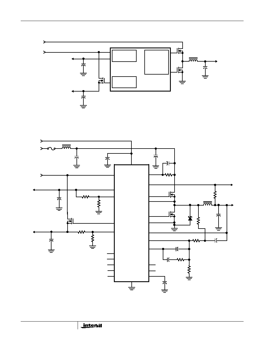
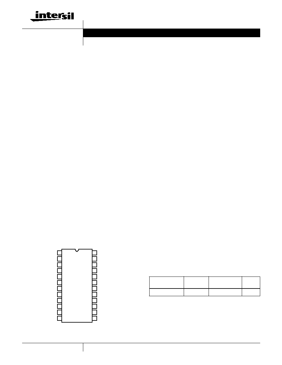
Electrical Specifications
Recommended Operating Conditions, Unless Otherwise Noted. Refer to Figures 1, 2 and 3
PARAMETER
SYMBOL
TEST CONDITIONS
MIN
TYP
MAX
UNITS
VCC SUPPLY CURRENT
Nominal Supply
I
CC
UGATE1, DRIVE3, LGATE1, and VOUT2 Open
-
8
-
mA
POWER-ON RESET
Rising VCC Threshold
V
OCSET
= 4.5V
8.6
-
10.4
V
Falling VCC Threshold
V
OCSET
= 4.5V
8.2
-
10.2
V
Rising VIN2 Under-Voltage Threshold
2.45
2.55
2.65
V
VIN2 Under-Voltage Hysteresis
-
100
-
mV
Rising V
OCSET1
Threshold
-
1.25
-
V
OSCILLATOR
Free Running Frequency
RT = OPEN
185
200
215
kHz
Total Variation
6k
< RT to GND < 200k
-15
-
+15
%
Ramp Amplitude
V
OSC
RT = Open
-
1.9
-
V
P-P
REFERENCE AND DAC
DAC(VID0-VID4) Input Low Voltage
-
-
0.8
V
DAC(VID0-VID4) Input High Voltage
2.0
-
-
V
DACOUT Voltage Accuracy
-1.0
-
+1.0
%
Reference Voltage (Pin FB2 and FB3)
1.240
1.265
1.290
V
LINEAR REGULATOR
Regulation
10mA < I
VOUT2
< 150mA
-2.5
-
2.5
%
Under-Voltage Level
FB2
UV
FB2 Rising
-
75
87
%
Under-Voltage Hysteresis
-
6
-
%
Over-Current Protection
180
230
-
mA
Over-Current Protection During Start-Up
560
700
-
mA
LINEAR CONTROLLER
Regulation
VSEN3 = DRIVE3, 0 < I
DRIVE3
< 20mA
-2.5
-
2.5
%
Under-Voltage Level
FB3
UV
FB3 Rising
-
75
87
%
Under-Voltage Hysteresis
-
6
-
%
Output Drive Current
I
DRIVE3
VIN2 - V
OUT3
> 1.5V
20
40
-
mA
DRIVE3 Source Current
VIN2 - DRIVE3 > 0.6V
20
40
-
mA
HIP6018B
2-242
PWM CONTROLLER ERROR AMPLIFIER
DC Gain
-
88
-
dB
Gain-Bandwidth Product
GBWP
-
15
-
MHz
Slew Rate
SR
COMP = 10pF
-
6
-
V/
µ
s
PWM CONTROLLER GATE DRIVER
Upper Drive Source
I
UGATE
VCC = 12V, V
UGATE1
(or V
GATE2
) = 6V
-
1
-
A
Upper Drive Sink
R
UGATE
V
UGATE1-PHASE1
= 1V
-
1.7
3.5
Lower Drive Source
I
LGATE
VCC = 12V, V
LGATE1
= 1V
-
1
-
A
Lower Drive Sink
R
LGATE
V
LGATE1
= 1V
-
1.4
3.0
PROTECTION
V
OUT1
Over-Voltage Trip
VSEN1 Rising
112
115
118
%
FAULT Sourcing Current
I
OVP
V
FAULT
= 10V
10
14
-
mA
OCSET1 Current Source
I
OCSET
V
OCSET
= 4.5V
DC
170
200
230
µ
A
Soft-Start Current
I
SS
-
11
-
µ
A
Chip Shutdown Soft-Start Threshold
-
-
1.0
V
POWER GOOD
V
OUT1
Upper Threshold
VSEN1 Rising
108
-
110
%
V
OUT1
Under Voltage
VSEN1 Rising
92
-
94
%
V
OUT1
Hysteresis (VSEN1 / DACOUT)
Upper/Lower Threshold
-
2
-
%
PGOOD Voltage Low
V
PGOOD
I
PGOOD
= -4mA
-
-
0.5
V
Electrical Specifications
Recommended Operating Conditions, Unless Otherwise Noted. Refer to Figures 1, 2 and 3 (Continued)
PARAMETER
SYMBOL
TEST CONDITIONS
MIN
TYP
MAX
UNITS
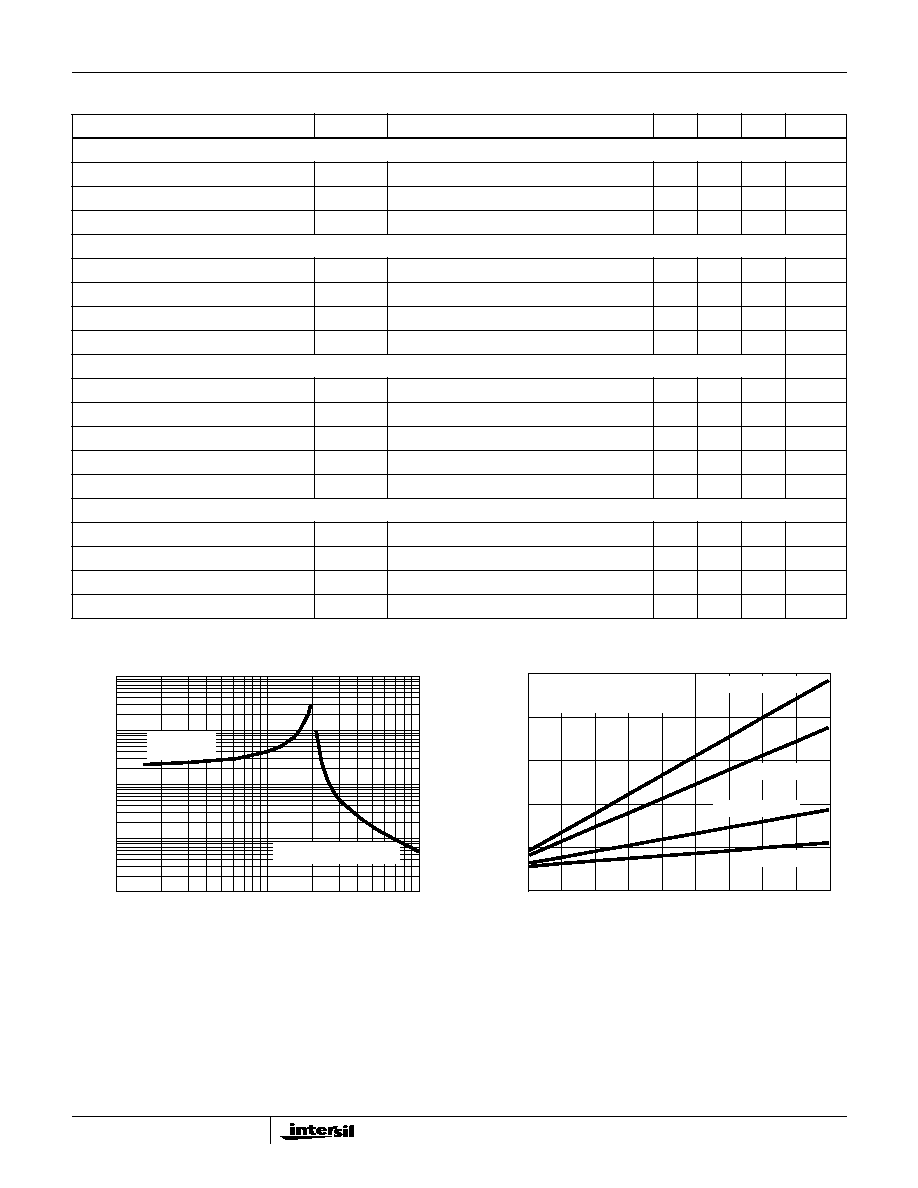
Typical Performance Curves
FIGURE 4. R
T
RESISTANCE vs FREQUENCY
FIGURE 5. BIAS SUPPLY CURRENT vs FREQUENCY
10
100
1000
SWITCHING FREQUENCY (kHz)
RESIST
ANCE (k
)
10
100
1000
R
T
PULLUP
TO +12V
R
T
PULLDOWN TO V
SS
100
200
300
400
500
600
700
800
900 1000
0
20
40
60
80
100
SWITCHING FREQUENCY (kHz)
I
CC
(mA)
C
UGATE1
= C
LGATE1
= C
GATE
C
GATE
= 4800pF
C
GATE
= 3600pF
C
GATE
= 1500pF
C
GATE
= 660pF
V
VCC
= 12V, V
IN
= 5V
HIP6018B