 | –≠–ª–µ–∫—Ç—Ä–æ–Ω–Ω—ã–π –∫–æ–º–ø–æ–Ω–µ–Ω—Ç: HIP6020A | –°–∫–∞—á–∞—Ç—å:  PDF PDF  ZIP ZIP |
4-1
TM
File Number
4735
CAUTION: These devices are sensitive to electrostatic discharge; follow proper IC Handling Procedures.
1-888-INTERSIL or 321-724-7143
|
Copyright
©
Intersil Corporation 1999
HIP6020A
Advanced Dual PWM and Dual Linear
Power Controller
The HIP6020A provides the power control and protection for
four output voltages in high-performance, graphics intensive
microprocessor and computer applications. The IC
integrates two PWM controllers and two linear controllers, as
well as the monitoring and protection functions into a 28-pin
SOIC package. One PWM controller regulates the
microprocessor core voltage with a synchronous-rectified
buck converter. The second PWM controller supplies the
computer system's AGP 1.5V or 3.3V bus power with a
standard buck converter. The linear controllers regulate
power for the 1.5V GTL bus and the 1.8V power for the
North/South Bridge core voltage and/or cache memory
circuits.
The HIP6020A includes an Intel-compatible, TTL 5-input
digital-to-analog converter (DAC) that adjusts the core PWM
output voltage from 1.3V
DC
to 2.05V
DC
in 0.05V steps and
from 2.1V
DC
to 3.5V
DC
in 0.1V increments. The precision
reference and voltage-mode control provide
±
1% static
regulation. The second PWM controller's output is user-
selectable, through a TTL-compatible signal applied at the
SELECT pin, for levels of 1.5V (
±
3%) or fully ON switch. The
linear regulators use external N-Channel MOSFETs or
bipolar NPN pass transistors to provide output voltages of
1.5V
±
3% (V
OUT3
) and 1.8V
±
3% (V
OUT4
).
The HIP6020A monitors all the output voltages. A single
Power Good signal is issued when the core is within 10% of
the DAC setting and all other outputs are above their under-
voltage levels. Additional built-in over-voltage protection for
the core output uses the lower MOSFET to prevent output
voltages above 115% of the DAC setting. The PWM
controllers' over-current function monitors the output current
by using the voltage drop across the upper MOSFET's
r
DS(ON)
, eliminating the need for a current sensing resistor.
Features
∑ Provides 4 Regulated Voltages
- Microprocessor Core, AGP Bus, North/South Bridge
and/or Cache Memory, and GTL Bus Power
∑ Drives N-Channel MOSFETs
∑ Linear Regulator Drives Compatible with both MOSFET
and Bipolar Series Pass Transistors
∑ Simple Single-Loop Control Designs
- Voltage-Mode PWM Control
∑ Fast PWM Converter Transient Response
- High-Bandwidth Error Amplifiers
- Full 0% to 100% Duty Ratios
∑ Excellent Output Voltage Regulation
- Core PWM Output:
±
1% Over Temperature
- AGP Bus PWM Output:
±
3% Over Temperature
(1.5V Setting Only)
- Other Outputs:
±
3% Over Temperature
∑ TTL-Compatible 5 Bit DAC Microprocessor Core Output
Voltage Selection
- Wide Range - 1.3V
DC
to 3.5V
DC
∑ Power-Good Output Voltage Monitor
∑ Over-Voltage and Over-Current Fault Monitors
- Switching Regulators Use MOSFET's r
DS(ON)
Sensing
∑ Small Converter Size
- Constant Frequency Operation
- 200kHz Free-Running Oscillator; Programmable From
50kHz to Over 1MHz
- Small External Component Count
Applications
∑ Motherboard Power Regulation for Computers
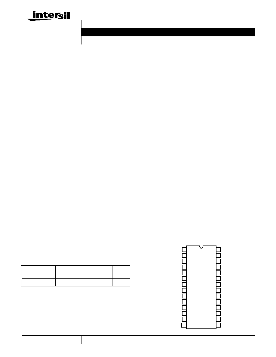
Pinout
HIP6020A (SOIC)
TOP VIEW
Ordering Information
PART NUMBER
TEMP.
RANGE (
o
C)
PACKAGE
PKG.
NO.
HIP6020ACB
0 to 70
28 Ld SOIC
M28.3
UGATE2
PHASE2
VID4
VID3
VSEN2
SELECT
SS
FAULT/RT
FB4
VCC
PGND
LGATE1
PHASE1
DRIVE3
COMP1
GND
VAUX
DRIVE4
UGATE1
28
27
26
25
24
23
22
21
20
19
18
17
16
15
1
2
3
4
5
6
7
8
9
10
11
12
13
14
PGOOD
VID2
OCSET2
VSEN1
FB3
VID1
VID0
OCSET1
FB1
Data Sheet
April 1999
4-2
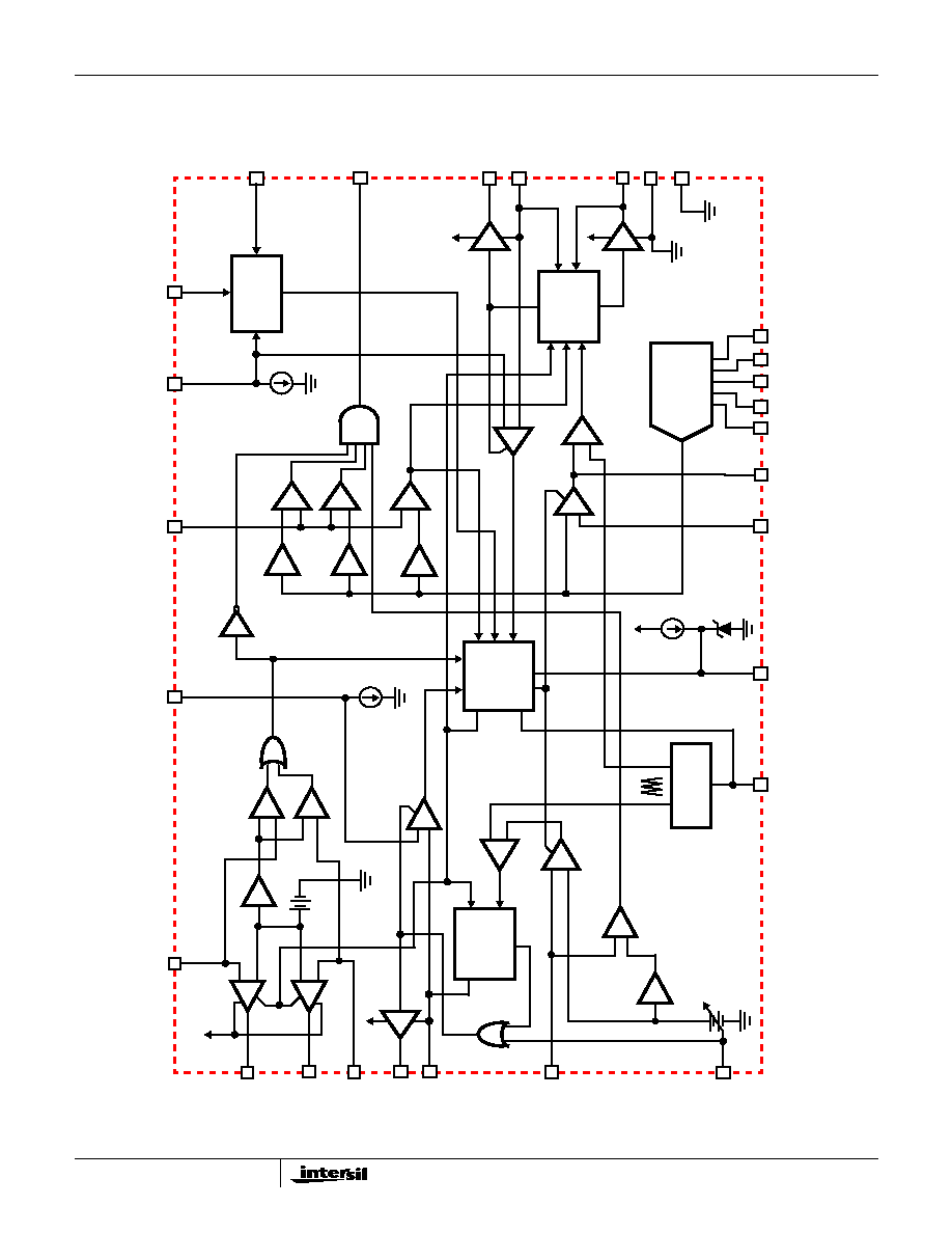
Bloc
k Dia
gram
SOFT-
START
INHIBIT
PWM
COMP1
ERROR
AMP1
VCC
PGOOD
PWM1
GND
VSEN1
OCSET1
VID0
VID1
VID2
VID3
FB1
COMP1
DACOUT
UGATE1
PHASE1
200
µ
A
28
µ
A
4.5V
+
-
+
-
+
-
+
-
VID4
LGATE1
PGND
DRIVE4
DRIVE3
FB3
+
-
INHIBIT
PWM2
UGATE2
PHASE2
ERROR
AMP2
PWM
COMP2
200
µ
A
OCSET2
VSEN2
FAULT / RT
+
-
+
-
GATE
CONTROL
+
-
1.26V
+
-
POWER-ON
RESET (POR)
TTL D/A
CONVERTER
(DAC)
OSCILLATOR
+
-
+
-
GATE
CONTROL
VCC
VCC
VCC
VCC
& FAULT
LOGIC
SS
1.5V
SYNCH
DRIVE
DRIVE1
DRIVE2
+
-
+
+
-
UNDER-
VOLTAGE
FB4
LINEAR
FAULT
OV
LUV
OC2
OC1
-
or
3.3V
+
-
SELECT
+
-
VAUX
VAUX
0.75
x
0.75
x
0.90
x
1.10
x
1.15
x
HIP6020A
4-3
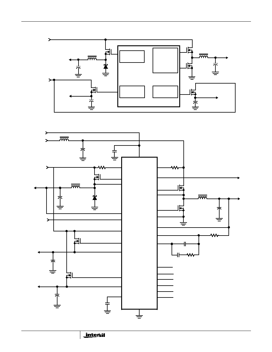
Simplified Power System Diagram
Typical Application
PWM1
+5V
IN
V
OUT1
Q1
Q2
Q3
V
OUT2
Q4
V
OUT3
V
OUT4
PWM2
LINEAR
LINEAR
HIP6020A
CONTROLLER
CONTROLLER
CONTROLLER
CONTROLLER
+3.3V
IN
Q5
VID1
VID2
VID3
VID4
SS
GND
VCC
+5V
IN
VID0
+12V
IN
V
OUT1
PGND
VSEN1
PGOOD
LGATE1
UGATE1
OCSET1
PHASE1
Q1
Q2
POWERGOOD
FB1
COMP1
1.3V TO 3.5V
SELECT
UGATE2
PHASE2
Q3
CR2
VSEN2
DRIVE3
FB3
FB4
C
OUT4
1.5V
1.8V
C
OUT3
C
OUT2
C
IN
C
OUT1
Q4
L
OUT2
L
OUT1
HIP6020A
V
OUT2
V
OUT3
V
OUT4
1.5V OR 3.3V
FAULT / RT
C
SS
Q5
TYPEDET
L
IN
DRIVE4
VAUX
OCSET2
+3.3V
IN
HIP6020A
4-4
Absolute Maximum Ratings
Thermal Information
Supply Voltage, V
CC
. . . . . . . . . . . . . . . . . . . . . . . . . . . . . . . . +15V
PGOOD, RT/FAULT, DRIVE, PHASE, and
GATE Voltage . . . . . . . . . . . . . . . . . . . GND - 0.3V to V
CC
+ 0.3V
Input, Output or I/O Voltage . . . . . . . . . . . . . . . . . . GND -0.3V to 7V
ESD Classification . . . . . . . . . . . . . . . . . . . . . . . . . . . . . . . . Class 1
Recommended Operating Conditions
Supply Voltage, V
CC
. . . . . . . . . . . . . . . . . . . . . . . . . . . +12V
±
10%
Ambient Temperature Range . . . . . . . . . . . . . . . . . . . . 0
o
C to 70
o
C
Junction Temperature Range . . . . . . . . . . . . . . . . . . . 0
o
C to 125
o
C
Thermal Resistance (Typical, Note 1)
JA
(
o
C/W)
SOIC Package. . . . . . . . . . . . . . . . . . . . . . . . . . . . .
70
Maximum Junction Temperature (Plastic Package) . . . . . . . .150
o
C
Maximum Storage Temperature Range . . . . . . . . . . -65
o
C to 150
o
C
Maximum Lead Temperature (Soldering 10s) . . . . . . . . . . . . .300
o
C
(SOIC - Lead Tips Only)
Electrical Specifications
Recommended Operating Conditions, Unless Otherwise Noted. Refer to Figures 1, 2 and 3
PARAMETER
SYMBOL
TEST CONDITIONS
MIN
TYP
MAX
UNITS
VCC SUPPLY CURRENT
Nominal Supply Current
I
CC
UGATE1, LGATE1, UGATE2, DRIVE3, and
DRIVE4 Open
-
9
-
mA
POWER-ON RESET
Rising VCC Threshold
V
OCSET
= 4.5V
-
-
10.4
V
Falling VCC Threshold
V
OCSET
= 4.5V
8.2
-
-
V
Rising VAUX Threshold
V
OCSET
= 4.5V
-
2.5
-
V
VAUX Threshold Hysteresis
V
OCSET
= 4.5V
-
0.5
-
V
Rising V
OCSET1
Threshold
-
1.26
-
V
OSCILLATOR
Free Running Frequency
F
OSC
RT = OPEN
185
200
215
kHz
Total Variation
6k
< RT to GND < 200k
-15
-
+15
%
Ramp Amplitude
V
OSC
RT = Open
-
1.9
-
V
P-P
DAC AND STANDARD BUCK REGULATOR REFERENCE
DAC(VID0-VID4) Input Low Voltage
0.8
V
DAC(VID0-VID4) Input High Voltage
2.0
V
DACOUT Voltage Accuracy
-1.0
-
+1.0
%
PWM2 Reference Voltage
SELECT < 0.8V
-
1.5
-
V
PWM2 Reference Voltage Tolerance
-
3
-
%
LINEAR REGULATORS (V
OUT3
AND V
OUT4
)
Regulation
-
3
-
%
FB3 Regulation Voltage
VREG
3
-
1.5
-
V
FB4 Regulation Voltage
VREG
4
-
1.8
-
V
FB3,4 Under-Voltage Level
FB
UV
FB Rising
-
75
-
%
FB3,4 Under-Voltage Hysteresis
7
%
Output Drive Current
VAUX-V
DRIVE
> 0.6V
20
40
-
mA
SYNCHRONOUS PWM CONTROLLER ERROR AMPLIFIER
DC Gain
-
88
-
dB
Gain-Bandwidth Product
GBWP
-
15
-
MHz
Slew Rate
SR
COMP1 = 10pF
-
6
-
V/
µ
s
HIP6020A
4-5
PWM CONTROLLERS GATE DRIVERS
UGATE1,2 Source
I
UGATE
VCC = 12V, V
UGATE1
(or V
UGATE2
) = 6V
-
1
-
A
UGATE1,2 Sink
R
UGATE
V
GATE-PHASE
= 1V
-
1.7
3.5
LGATE Source
I
LGATE
VCC = 12V, V
LGATE1
= 1V
-
1
-
A
LGATE Sink
R
LGATE
V
LGATE
= 1V
-
1.4
3.0
PROTECTION
VSEN1 Over-Voltage (VSEN1/DACOUT)
VSEN1 Rising
-
115
120
%
FAULT Sourcing Current
I
OVP
V
FAULT/RT
= 2.0V
-
8.5
-
mA
OCSET1,2 Current Source
I
OCSET
V
OCSET
= 4.5V
DC
170
200
230
µ
A
Soft-Start Current
I
SS
-
28
-
µ
A
VSEN2 Under-Voltage Threshold
SELECT < 0.8V
-
75
-
%
SELECT > 2.0V
-
2.475
-
V
VSEN2 Under-Voltage Hysteresis
SELECT < 0.8V
-
7
-
%
SELECT > 2.0V
-
0.231
-
V
POWER GOOD
VSEN1 Upper Threshold
(VSEN1/DACOUT)
VSEN1 Rising
108
-
110
%
VSEN1 Under-Voltage
(VSEN1/DACOUT)
VSEN1 Rising
92
-
94
%
VSEN1 Hysteresis (VSEN1/DACOUT)
Upper/Lower Threshold
-
2
-
%
PGOOD Voltage Low
V
PGOOD
I
PGOOD
= -4mA
-
-
0.8
V
Electrical Specifications
Recommended Operating Conditions, Unless Otherwise Noted. Refer to Figures 1, 2 and 3 (Continued)
PARAMETER
SYMBOL
TEST CONDITIONS
MIN
TYP
MAX
UNITS
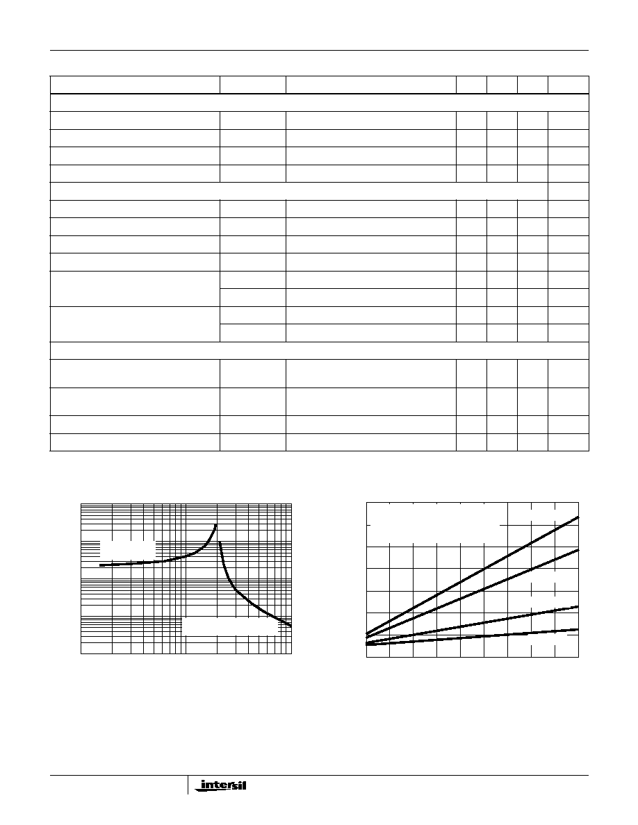
Typical Performance Curves
FIGURE 1. R
T
RESISTANCE vs FREQUENCY
FIGURE 2. BIAS SUPPLY CURRENT vs FREQUENCY
10
100
1000
SWITCHING FREQUENCY (kHz)
RESIST
ANCE (k
)
10
100
1000
R
T
PULLUP
TO +12V
R
T
PULLDOWN TO V
SS
100
200
300
400
500
600
700
800
900
1000
I
CC
(mA)
SWITCHING FREQUENCY (kHz)
140
120
100
80
60
40
20
0
C = 660pF
C = 1500pF
C = 3600pF
C = 4800pF
C
UGATE1
= C
UGATE2
= C
LGATE1
= C
V
IN
= 5V ; SELECT < 0.8V
V
CC
= 12V
HIP6020A